EP0700042A1 - Dispositif de traitement de signaux - Google Patents
Dispositif de traitement de signaux Download PDFInfo
- Publication number
- EP0700042A1 EP0700042A1 EP95113168A EP95113168A EP0700042A1 EP 0700042 A1 EP0700042 A1 EP 0700042A1 EP 95113168 A EP95113168 A EP 95113168A EP 95113168 A EP95113168 A EP 95113168A EP 0700042 A1 EP0700042 A1 EP 0700042A1
- Authority
- EP
- European Patent Office
- Prior art keywords
- digital signal
- input digital
- detecting
- data
- signal
- Prior art date
- Legal status (The legal status is an assumption and is not a legal conclusion. Google has not performed a legal analysis and makes no representation as to the accuracy of the status listed.)
- Ceased
Links
Images


Classifications
-
- H—ELECTRICITY
- H04—ELECTRIC COMMUNICATION TECHNIQUE
- H04L—TRANSMISSION OF DIGITAL INFORMATION, e.g. TELEGRAPHIC COMMUNICATION
- H04L25/00—Baseband systems
- H04L25/38—Synchronous or start-stop systems, e.g. for Baudot code
- H04L25/40—Transmitting circuits; Receiving circuits
- H04L25/49—Transmitting circuits; Receiving circuits using code conversion at the transmitter; using predistortion; using insertion of idle bits for obtaining a desired frequency spectrum; using three or more amplitude levels ; Baseband coding techniques specific to data transmission systems
- H04L25/497—Transmitting circuits; Receiving circuits using code conversion at the transmitter; using predistortion; using insertion of idle bits for obtaining a desired frequency spectrum; using three or more amplitude levels ; Baseband coding techniques specific to data transmission systems by correlative coding, e.g. partial response coding or echo modulation coding transmitters and receivers for partial response systems
-
- G—PHYSICS
- G11—INFORMATION STORAGE
- G11B—INFORMATION STORAGE BASED ON RELATIVE MOVEMENT BETWEEN RECORD CARRIER AND TRANSDUCER
- G11B20/00—Signal processing not specific to the method of recording or reproducing; Circuits therefor
- G11B20/10—Digital recording or reproducing
- G11B20/10009—Improvement or modification of read or write signals
Definitions
- This invention relates to a signal processing device and more particularly to control over the level of a digital signal reproduced from a recording medium.
- PR(1,0,-1) system a detecting method called a "partial response 1,0,-1 method of system” (hereinafter referred to as the PR(1,0,-1) system) has come to be popularly employed in detecting reproduced data.
- Fig. 1 is a block diagram showing by way of example the arrangement of the reproduction system of a digital VTR of the above-stated kind.
- a digital signal recorded on a magnetic tape 1 is reproduced by a magnetic head 2.
- the amplitude of the reproduced digital signal is controlled by a gain control amplifier (GCA) 3 and is then supplied to a reproduction equalizing circuit 4.
- GCA gain control amplifier
- the reproduction frequency characteristic of the magnetic head 2 is as shown in Fig. 2(a).
- a differential characteristic is obtained for a low frequency band while an attenuating characteristic is obtained for a high frequency band due to losses of varied kinds.
- the reproduction equalizing circuit 4 which has a frequency characteristic as shown in Fig. 2(b) is used for equalization to make the frequency characteristic into a cosine roll-off characteristic as shown in Fig. 2(c).
- the cosine roll-off characteristic minimizes a waveform interference at a data detecting point.
- the recorded data is restored by carrying out a binary discriminating action on the equalized signal.
- the equalizing process described above is called an integral equalization and a process of detecting the polarity of the integrally equalized signal by means of comparator or the like is called integral detection.
- the eye pattern of the signal which is integrally equalized in the above-stated manner becomes as shown in Fig. 3(a).
- This clock signal is generated by a PLL (phase-locked loop) which consists of a phase detecting circuit 22, a loop filter 21 and a voltage controlled oscillator 20 (hereinafter referred to as VCO).
- phase difference between the clock signal generated by the VCO 20 and a signal outputted from the reproduction equalizing circuit 4 is detected by the phase detecting circuit 22.
- a phase difference signal thus obtained is supplied through the loop filter 21 to the VCO 20 to apply a phase lock by controlling the oscillation frequency of the VCO 20 in such a way as to make the phase difference almost zero at the phase detecting circuit 22.
- the phase response characteristics of the PLL such as the frequency characteristic of the loop filter 21, a gain, the sensitivity of the VCO 20, etc., are set in such a way as to adequately absorb jitters generated by the head-tape system of the VTR and not to readily respond to noises of varied kinds.
- AGC loop automatic gain control loop
- the amplitude detecting circuit 23 includes a detection circuit which is arranged to detect the peak value of the signal equalized. The detected peak value is amplified when only a low band component of the signal is passed by the loop filter 24 and is supplied to the control terminal of the GCA 3. The gain of the GCA 3 is thus controlled to keep the amplitude detection output almost constant.
- the integrally equalized signal is sampled by the A/D converter 5 under the control of the clock signal generated by the above-stated PLL and is converted into a digital signal which consists of a plurality of bits per sample thus obtained.
- the signal reproduced by the head 2 is of course in the form of a digital signal. However, the amplitude of the digital signal varies in an analog manner. Therefore, the A/D converter 5 converts the reproduced signal again into a digital signal consisting of a plurality of bits per sample as mentioned above.
- the reproduced signal which has been converted into the digital signal is delayed by a delay circuit 6 as much as the length of two clock pulses to obtain a delayed signal.
- the delayed signal is subtracted from the original signal by a subtracter 7.
- the integrally equalized waveform is converted into a waveform having the characteristic of PR(1,0,-1) and its eye pattern has a ternary value as shown in Fig. 3(b).
- This signal of the PR(1,0,-1) characteristic is supplied to a Viterbi decoding circuit 8 to be restored to the original form of binary signal of "1" and "0" by maximum likelihood decoding.
- the signal is outputted as a digital signal having one bit per sample.
- the combination of the PR(1,0,-1) method and the Viterbi decoding is often used for a digital VTR arranged to perform high density magnetic recording.
- the use of this combination enables the VTR to avoid the degradation of the low band characteristic of a magnetic recording system, such as deteriorated S/N ratio and distorted waveform, and to minimize transmission errors.
- the reproduced data decoded by the Viterbi decoding circuit 8 is supplied to an error correcting circuit (ECC) 9 to have any error generated through a transmission route corrected by using parity data added to the signal at the time of recording.
- ECC error correcting circuit
- the image decoding circuit 10 expands the amount of information of the reproduced data which has been compressed at the time of recording and then supplies its output to a D/A converter 11.
- the D/A converter 11 then converts the input digital data into analog data.
- the analog data thus obtained is outputted through an output terminal 12.
- the conventional VTR described above is arranged to peak-detect the amplitude of the equalized signal and to perform control in such a way as to keep its detection output unvarying.
- the arrangement of carring out the peak detection tends to keep unvarying an amplitude obtained at some point other than a desired detection point at which the amplitude is desired to be kept unvarying.
- the peak voltage of the point other than the detection point varies too much depending on the pattern of data.
- a low frequency noise is superimposed on the waveform.
- the detected amplitude is inevitably affected by the low frequency noise to make it difficult to keep the amplitude level unvarying.
- a digital signal processing device includes pattern detecting means for detecting a specific pattern included in an input digital signal, level detecting means for detecting the level of the input digital signal on the basis of an output of the pattern detecting means, and level control means for controlling the level of the input digital signal according to the output of the level detecting means.
- Fig. 1 is a block diagram showing the arrangement of a digital VTR.
- Figs. 2(a), 2(b) and 2(c) show the characteristics of reproduced signals.
- Figs. 3(a) and 3(b) show eye patterns of reproduced signals.
- Fig. 4 is a block diagram showing a digital VTR arranged as an embodiment of this invention.
- Fig. 5 is a block diagram showing the arrangement of a digital phase detecting circuit of the VTR shown in Fig. 4.
- Fig. 6 shows the operation of the embodiment of this invention.
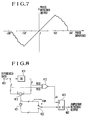
- Fig. 7 shows the phase comparing characteristic of the circuit shown in Fig. 5.
- Fig. 8 is a block diagram showing the arrangement of a digital amplitude detecting circuit of the VTR shown in Fig. 4.
- Fig. 9 is a block diagram showing a digital VTR arranged as another embodiment of this invention.
- Fig. 10 is a block diagram showing the arrangement of a digital phase-and-amplitude detecting circuit included in the VTR of Fig. 9.
- Fig. 11 is a block diagram showing another example of arrangement of the digital phase-and-amplitude detecting circuit of the VTR of Fig. 9.
- Fig. 12 is a block diagram showing a further example of arrangement of the digital phase-and-amplitude detecting circuit of the VTR of Fig. 9.
- Fig. 4 shows in a block diagram the arrangement of a reproduction system included in a digital VTR which is an embodiment of this invention.
- Fig. 4 all the parts of the VTR that act in the same manner as those of Fig. 1 are indicated by the same reference numerals and the details of them are omitted from the following description.
- a digital phase detecting circuit 30 consists of a pattern detecting circuit 31 and a sample-and-hold circuit 32.
- a digital signal obtained by the A/D converter 5 is supplied to the pattern detecting circuit 31.
- the pattern detecting circuit 31 outputs a signal according to a pattern detected.
- the A/D converter 5 converts a reproduced signal into a digital signal consisting of four bits.
- the sample-and-hold circuit 32 To the sample-and-hold circuit 32 is supplied a signal of the PR(1,0,-1) system.
- the PR(1,0,-1) signal is sampled and held under the control of the output of the pattern detecting circuit 31.
- the pattern detecting circuit 31 is arranged to detect a plurality of patterns appearing in an input signal as will be described later herein. With the plurality of patterns thus detected, a signal which corresponds to a phase difference between the reproduced signal and the clock signal used for analog-to-digital (A/D) conversion is obtained at the output of the sample-and-hold circuit 32.
- Fig. 5 is a block diagram showing in detail the arrangement of the digital phase detecting circuit 30.
- delay circuits 311 to 314 are arranged to delay the digital signal 301 which is obtained by A/D conversion for every clock pulse.
- a decoder 315 is composed of a logical operation circuit which is arranged to detect a specific pattern from the outputs of the delay circuits 311 to 314. These elements 311 to 316 jointly form the pattern detecting circuit 31.
- a subtracter 316 is arranged to subtract the output of the delay circuit 313 from the output of the delay circuit 311.
- a negation circuit 321 is arranged to negate the output of the subtracter 316.
- a switch 322 is arranged to perform switching between the output of the subtracter 316 and that of the negation circuit 321 in accordance with a signal s which is outputted from the decoder 315.
- a latch circuit 323 is arranged to sample and hold the output of the switch 322 in accordance with a signal ph outputted from the decoder 315 and to output it as a phase detection signal.
- the A/D converted reproduced signal is inputted to the delay circuit 301 to be delayed by the delay circuits 311 to 314 one after another.
- the outputs of the delay circuits 311 and 313 are supplied to the subtracter 316.
- the subtracter 316 then outputs a PR(1,0,-1) signal.
- the MSBs (most significant bits) of the data inputted to and of the data outputted from the delay circuits 311 to 314, each data consisting of four bits, are here assumed to be a, b, c, d and e, respectively.
- the MSBs a, b, c, d and e become a binary data train obtained by integrally detecting a reproduced data train.
- This data train is inputted to the decoder 315, which then detects from the input data train a specific pattern through a logical operation and thus obtains the signals s and ph.
- the signal s controls the switch 322 to selectively output the output of the subtracter 316 or the signal obtained by inverting the sign of the output of the subtracter 316 through the sign inverting circuit 321.
- the signal ph is supplied to a terminal E ⁇ of the latch circuit 323 to control the latch circuit 323 in such a way as to sample and hold the output of the switch 322 at the timing of the signal ph.
- Fig. 3(b) shows the eye pattern of the PR(1,0,-1) signal as mentioned above.
- the eye pattern has a ternary value at the data detecting point.
- the zero-cross point of the eye pattern indicates that a signal passing the zero-cross point has an inclination proportional to a phase difference between the data and the detecting point.
- This inclination has either a positive or negative value.
- the decoder 315 is, therefore, arranged to obtain the signal s to determine this inclination to be a positive or negative inclination and to obtain the signal ph to determine the zero-cross point, so that a specific pattern included in the reproduced signal is detected by carrying out a predetermined logical operation.
- the level of the phase detection output 302 of the digital phase detecting circuit 30 is in proportion to the phase difference between the data and the data detecting point.
- the inclination at the zero-cross point takes-various values and the inclination of the phase comparison characteristic (phase detection sensitivity) also varies according to the pattern of the data.
- the variations present no problem within the loop of the PLL because, in the PLL, variations take place only in the average value of loop gains.
- this embodiment is arranged to obtain and output the signals s and ph by detecting a specific pattern through a logical operation from an integrally equalized data train.
- Fig. 6 shows by way of example a truth table of the signals s and ph.
- Fig. 6 there are shown logics of an output "b - d" of the subtracter 316 and the signals s and ph with respect to the integrally detected data a, b, c, d and e.
- the signal s indicates whether the inclination is positive or negative while the signal ph indicates whether the output "b - d" corresponds to the zero-cross point, that is, whether the data of the specific pattern is inputted.
- phase detection output 302 varies in proportion to the phase difference between the data and the clock signal. A phase deviation results in data sampling at a wrong timing by the digital phase detecting circuit 30. Then, the phase detection output 302 is supplied via the loop filter 21 to the VCO 20 to cause the oscillation frequency of the VCO 20 to vary in such a way as to eliminate the phase difference between the reproduced signal and the clock signal, so that the operation of the device can be soon pulled into a phase locked state.
- Fig. 7 shows the phase comparison characteristic of the embodiment. As shown, the phase comparison characteristic is linear over a range of about ⁇ 100° and thus gives a sufficient phase lock range to the PLL.
- PR(1,0,-1) data sampled at the input timing of the clock signal can be controlled to be obtained stably at the zero-cross point. Therefore, the data can be accurately detected with the locking phase of the PLL automatically following the data detecting point. Further, with the loop filter 20 arranged to perform a digital operation, there arises no DC offset or the like which has been a problem with an analog circuit. As a result, it becomes no longer necessary to adjust the PLL of the device.
- the output of the VCO 20 is supplied not only to the A/D converter 5 but also to other applicable circuits of the apparatus as an operating clock signal.
- a digital amplitude detecting circuit 40 is next described with reference to Fig. 8, which is a block diagram showing in detail the arrangement of the digital amplitude detecting circuit 40.
- a delay circuit 411 is arranged to delay input data as much as the length of two clock pulses.
- An EXOR circuit 412 is arranged to obtain an exclusive OR of the input and output data of the delay circuit 411.
- a subtracter 413 is arranged to obtain data of the PR(1,0,-1) system by subtracting the output data from the input data.
- Elements 421, 422 and 423 are arranged to act in the same manner as the sign inverting circuit 321, the switch 322 and the latch circuit 323 of Fig. 5, except that the switch 422 is controlled by a signal "sign" which will be described later herein.
- the PR(1,0,-1) data which is outputted from the subtracter 413 is of the eye pattern shown in Fig. 3(b).
- two values obtained at points other than the zero-cross point indicate the amplitude of the reproduced data.
- the embodiment detects the amplitude of the detected data by detecting a specific pattern with the EXOR circuit 412 and by sampling and holding the data when the output of the subtracter 413 is at points other than the zero-cross point.
- the same method as the above-stated method used by the phase detecting circuit 30 is used.
- a specific pattern obtained when the output of the subtracter 413 is at points other than the zero-cross point is detected by means of the EXOR circuit 412 and a signal ah is supplied to the latch circuit 423.
- the latch circuit 423 then latches and output the data outputted from the switch 422 at the input timing of the signal ah.
- the logic of the signal ah is shown at a column “ah” in Fig. 6.
- the latch circuit 423 acts when the signal ah is "0".
- the sign (MSB) of the PR(1,0,-1) data may be used (middle data of a column "b - d" in the case of Fig. 6).
- the sign (MSB) of the PR(1,0,-1) data may be used (middle data of a column "b - d" in the case of Fig. 6).
- the sign (MSB) of the PR(1,0,-1) data may be used (middle data of a column "b - d" in the case of Fig. 6).
- the inverted data of d or b may be used.
- the amplitude of the reproduced signal is detected by detecting a specific pattern from the reproduced data when the PR(1,0,-1) data indicates an amplitude and by sampling and holding the PR(1,0,-1) data on the basis of the detection output. Therefore, an amplitude obtained at the data detecting point can be accurately detected.
- the AGC loop With the loop filter 24 arranged to be a digital circuit, like in the case of the PLL described in the foregoing, the AGC loop also can be completely digitized. This arrangement obviates the necessity of any adjustment work, etc., that have been necessary for an analog circuit.
- the data detecting point is detected by means of a simple logic circuit, the level of the detecting point can be accurately detected with simple arrangement.
- pattern detecting circuits are provided respectively in the phase detecting circuit 30 and in the amplitude detecting circuit 40.
- Fig. 9 shows the arrangement of a reproduction system of a digital VTR which is the second embodiment of this invention.
- a phase-and-amplitude detecting circuit 50 is arranged to perform both a phase detecting action and an amplitude detecting action.
- this circuit 50 all other parts of the second embodiment are identical with Fig. 4.
- phase-and-amplitude detecting circuit 50 Details of the phase-and-amplitude detecting circuit 50 are as shown by way of example in Fig. 10.
- each of delay circuits 511 to 514 is arranged to delay input data 501 as much as the length of one clock pulse in the same manner as in the case of the delay circuits described in the foregoing.
- a decoder 515 is arranged to detect whether or not the PR(1,0,-1) data is at a zero-cross point by detecting a specific pattern and then to output signals s, ph and ah.
- the elements 511 to 516 jointly form a pattern detecting circuit 51.
- a sign inverting circuit 521 is arranged to invert the sign of the output of a subtracter 516 and to output the result of inversion.
- Switches 522 and 523 are arranged to selectively output the data inputted to and outputted from the sign inverting circuit 521.
- Latch circuits 524 and 525 are arranged to latch the data outputted from the switches 522 and 523 respectively at the timing of the signals ph and ah. These elements 521 to 525 jointly form a sample-and-hold circuit 52.
- the switch 522 is controlled by the signal s and the switch 523 by the signal "sign".
- a reference numeral 502 denotes a phase detection output and a numeral 503 an amplitude detection output.
- the phase-and-amplitude detecting circuit 50 operates in about the same manner as the foregoing embodiment.
- the decoder 515 detects by the above-mentioned logical operation a specific pattern which indicates that the data outputted from the subtracter 516 is at the zero-cross point, the decoder 515 sends the signal ph to the latch circuit 524.
- the signal ph causes the PR(1,0,-1) data outputted from the switch 522 to be sampled and held.
- the decoder 515 sends the signal s which indicates the inclination of the detected data to the switch 522 to cause the switch 522 to select and output the data inputted to and outputted from the sign inverting circuit 521.
- the phase detection output 502 is smoothed by the loop filter 21 and is supplied to the VCO 20 to control the oscillation frequency of the VCO 20 as mentioned in the foregoing.
- the amplitude detection is performed as follows: When the decoder 515 detects a specific pattern which indicates that the output of the subtracter 516 is not at the zero-cross point on the basis of the data b and d, the decoder 515 sends the signal ah to the latch circuit 525. As a result, the PR(1,0,-1) data outputted from the switch 523 is sampled and held. The switch 523 acts under the control of the signal "sign" to select the data inputted to and outputted from the sign inverting circuit 521. The amplitude detection output 503 is smoothed by the loop filter 24 and is then supplied to the GCA 3 to control the level of the reproduced signal in the same manner as mentioned in the foregoing.
- the second embodiment is arranged to use a common pattern detecting circuit in detecting specific patterns and to detect both the phase and the amplitude on the basis of the detection outputs as described above, the embodiment not only accurately detects any phase deviation from the clock signal and the amplitude of the reproduced data at the data detecting point but also permits reduction in size of the circuit arrangement.
- this invention is not limited to digital VTRs but is also advantageously applicable to a system of transmitting and reproducing binary data, such as a communication system using radio waves or light, an optical disk, etc.
- a ternary value may be detected by some detecting system other than the PR(1,0,-1) system, such as a PR(1,-1) system or a PR(1,1) system, by arranging a phase-and-amplitude detecting circuit in a manner similar to the embodiment.
- the digital phase-and-amplitude detecting circuit 50 is arranged as shown in Fig. 11 or 12.
- the examples shown in Figs. 11 and 12 differ from the arrangement of Fig. 10 in that the subtracter 516 is arranged to obtain a difference between reproduced data and data delayed by the length of one clock pulse and that the decoder 515 has a different logic.
- the example shown in Fig. 11 uses only one delay circuit 511 and an EXOR gate 517 in place of the decoder 515.
- the signals ph and ah are obtained from data b and c which are the MSBs of the input and output of the delay circuit 511 while the data c is used also as the signal s.
- three delay circuits 511, 512 and 513 are used.
- the MSBs of the delay outputs of these delay circuits 511, 512 and 513 and the MSB of the reproduced data 501 are supplied as data a, b, c and d to the decoder 515.
- the decoder 515 then obtains the signals ph and s by carrying out a logical operation, in accordance with a formula shown in Fig. 12, and the signal ah by detecting the inversion output of the EXOR gate obtained from the data b and c.
- Each of the embodiments described is arranged to provide each detecting circuit with a delay circuit and a subtracter. However, this arrangement can be changed to arrange the delay circuit 6 and the subtracter 7 of Fig. 4 or 9 to be used in common with each of the detecting circuits by omitting the delay circuits and subtracters of them. This change permits further reduction in size of the apparatus.
- a specific pattern in the input digital signal is detected and the amplitude of the input digital signal is detected on the basis of a digital signal extracted according to the detection timing.
- the amplitude of the reproduced signal can be accurately detected at the detecting point of the data having the specific pattern.
- the level of the reproduced signal is controlled according to the amplitude of reproduced signal detected in the above-stated manner. Therefore, the level of the reproduced signal can be kept unvarying at the detecting point of the data, so that errors in the reproduced data can be lessened.
- the delayed data obtained by serially delaying the input digital data through delay means and the input digital signal are subjected to a binary discriminating and deciding process to obtain data of N bits.
- a logical operation is carried out using the N bit data.
- the results of an arithmetical operation carried out on two of the data outputted from the delay means are latched according to the result of logical operation.
- a latched value thus obtained is outputted as representing the amplitude of the input digital signal.
- An amplitude detection output is thus can be obtained directly from the input digital signal. Therefore, the level of the reproduced signal can be stably controlled.
- the arrangement not only obviates the necessity of adjustment work on the device and also lessens errors in processing the reproduced signal.
- a specific pattern included in the input digital signal is detected, the amplitude of the input digital signal is detected on the basis of a digital signal extracted according to the timing of detection of the specific pattern, and a clock signal is generated in synchronism with the input digital signal. Therefore, the amplitude of the reproduced signal can be accurately detected at the detecting point of the data having the specific pattern and the clock signal can be generated in a state of being phase-locked to the data detecting point.
- a device is arranged to detect the level of an input digital signal by detecting a specific pattern from the input digital signal and to control the level of the input digital signal according to a result of the level detection.
- the arrangement enables the device to accurately detect the amplitude of a reproduced signal obtained at the detecting point of data which has the specific pattern, to keep the level of the reproduced signal unvarying at the data detecting point and to lessen errors of reproduced data.
Landscapes
- Engineering & Computer Science (AREA)
- Signal Processing (AREA)
- Physics & Mathematics (AREA)
- Spectroscopy & Molecular Physics (AREA)
- Computer Networks & Wireless Communication (AREA)
- Signal Processing For Digital Recording And Reproducing (AREA)
- Control Of Amplification And Gain Control (AREA)
Applications Claiming Priority (2)
| Application Number | Priority Date | Filing Date | Title |
|---|---|---|---|
| JP20057594A JP3639618B2 (ja) | 1994-08-25 | 1994-08-25 | 信号処理装置 |
| JP200575/94 | 1994-08-25 |
Publications (1)
| Publication Number | Publication Date |
|---|---|
| EP0700042A1 true EP0700042A1 (fr) | 1996-03-06 |
Family
ID=16426622
Family Applications (1)
| Application Number | Title | Priority Date | Filing Date |
|---|---|---|---|
| EP95113168A Ceased EP0700042A1 (fr) | 1994-08-25 | 1995-08-22 | Dispositif de traitement de signaux |
Country Status (3)
| Country | Link |
|---|---|
| US (1) | US6374035B1 (fr) |
| EP (1) | EP0700042A1 (fr) |
| JP (1) | JP3639618B2 (fr) |
Cited By (1)
| Publication number | Priority date | Publication date | Assignee | Title |
|---|---|---|---|---|
| EP1126398A2 (fr) * | 2000-01-24 | 2001-08-22 | Kabushiki Kaisha Sankyo Seiki Seisakusho | Lecteur de carte magnétique et méthode de reproduction et de démodulation |
Families Citing this family (3)
| Publication number | Priority date | Publication date | Assignee | Title |
|---|---|---|---|---|
| JP2000149436A (ja) * | 1998-11-02 | 2000-05-30 | Sony Corp | ディジタル情報再生装置および再生方法 |
| JP2001357633A (ja) * | 2000-06-12 | 2001-12-26 | Mitsubishi Electric Corp | 情報再生装置および情報再生方法 |
| CN113933350B (zh) * | 2021-09-30 | 2023-12-22 | 深圳市中金岭南有色金属股份有限公司凡口铅锌矿 | 矿浆pH值检测方法、装置及计算机可读存储介质 |
Citations (4)
| Publication number | Priority date | Publication date | Assignee | Title |
|---|---|---|---|---|
| JPS5977608A (ja) * | 1982-10-27 | 1984-05-04 | Hitachi Ltd | 記録タイミング補正 |
| EP0538867A2 (fr) * | 1991-10-25 | 1993-04-28 | Sony Corporation | Boucle à verrouillage de phase commandé par la décision |
| US5265125A (en) * | 1990-11-16 | 1993-11-23 | Matsushita Electric Industrial Co., Ltd. | Signal detection apparatus for detecting digital information from PCM signal |
| WO1993023941A1 (fr) * | 1992-05-08 | 1993-11-25 | Cirrus Logic, Inc. | Detecteur d'impulsions numerique |
Family Cites Families (9)
| Publication number | Priority date | Publication date | Assignee | Title |
|---|---|---|---|---|
| JPS5665311A (en) * | 1979-10-27 | 1981-06-03 | Nippon Telegr & Teleph Corp <Ntt> | Magnetic recording and reproduction system for digital information |
| JPH03166839A (ja) * | 1989-11-27 | 1991-07-18 | Matsushita Electric Ind Co Ltd | ディジタル情報検出装置 |
| US5247397A (en) * | 1990-10-26 | 1993-09-21 | Sony Corporation | Method for magnetically recording digital video signals with specified ranges of the easy axis and the bias magnetic field |
| US5291499A (en) * | 1992-03-16 | 1994-03-01 | Cirrus Logic, Inc. | Method and apparatus for reduced-complexity viterbi-type sequence detectors |
| JP3292323B2 (ja) * | 1993-03-02 | 2002-06-17 | ソニー株式会社 | 情報再生装置 |
| US5430744A (en) * | 1993-09-30 | 1995-07-04 | International Business Machines Corporation | Method and means for detecting partial response waveforms using a modified dynamic programming heuristic |
| US5563864A (en) * | 1993-12-24 | 1996-10-08 | Seiko Epson Corporation | Information recording and reproducing apparatus |
| US5490091A (en) * | 1994-03-01 | 1996-02-06 | Guzik Technical Enterprises, Inc. | Histograms of processed noise samples for measuring error rate of a PRML data detection channel |
| US5544178A (en) * | 1994-06-10 | 1996-08-06 | Cirrus Logic, Inc. | Method and apparatus for encoding data in a PRML class-IV digital communication channel |
-
1994
- 1994-08-25 JP JP20057594A patent/JP3639618B2/ja not_active Expired - Fee Related
-
1995
- 1995-08-07 US US08/511,740 patent/US6374035B1/en not_active Expired - Fee Related
- 1995-08-22 EP EP95113168A patent/EP0700042A1/fr not_active Ceased
Patent Citations (4)
| Publication number | Priority date | Publication date | Assignee | Title |
|---|---|---|---|---|
| JPS5977608A (ja) * | 1982-10-27 | 1984-05-04 | Hitachi Ltd | 記録タイミング補正 |
| US5265125A (en) * | 1990-11-16 | 1993-11-23 | Matsushita Electric Industrial Co., Ltd. | Signal detection apparatus for detecting digital information from PCM signal |
| EP0538867A2 (fr) * | 1991-10-25 | 1993-04-28 | Sony Corporation | Boucle à verrouillage de phase commandé par la décision |
| WO1993023941A1 (fr) * | 1992-05-08 | 1993-11-25 | Cirrus Logic, Inc. | Detecteur d'impulsions numerique |
Non-Patent Citations (4)
| Title |
|---|
| F. DOLIVO: "Signal processing for high-density magnetic recording", COMPEURO '89 , PROCEEDINGS VLSI AND COMPUTER PERIPHERALS, 8 May 1989 (1989-05-08) - 12 May 1989 (1989-05-12), HAMBURG, pages 1/91 - 1/96, XP000044104 * |
| PATENT ABSTRACTS OF JAPAN vol. 16, no. 163 (P - 1341) 21 April 1992 (1992-04-21) * |
| PATENT ABSTRACTS OF JAPAN vol. 8, no. 188 (P - 297) 29 August 1984 (1984-08-29) * |
| W.L. ABBOTT AND J.M. CIOFFI: "Timing recovery for adaptive decision feedback equalization of the magnetic storage channel", GLOBECOM '90, 2 December 1990 (1990-12-02) - 5 December 1990 (1990-12-05), SAN DIEGO, pages 1794 - 1799, XP000218879 * |
Cited By (5)
| Publication number | Priority date | Publication date | Assignee | Title |
|---|---|---|---|---|
| EP1126398A2 (fr) * | 2000-01-24 | 2001-08-22 | Kabushiki Kaisha Sankyo Seiki Seisakusho | Lecteur de carte magnétique et méthode de reproduction et de démodulation |
| EP1126398A3 (fr) * | 2000-01-24 | 2002-08-21 | Kabushiki Kaisha Sankyo Seiki Seisakusho | Lecteur de carte magnétique et méthode de reproduction et de démodulation |
| US6570722B2 (en) | 2000-01-24 | 2003-05-27 | Kabushiki Kaisha Sankyo Seiki Seisakusho | Magnetic card reader and magnetic data reproduction method using signal peak point intervals |
| US6570723B2 (en) | 2000-01-24 | 2003-05-27 | Kabushiki Kaisha Sankyo Seiki Seisakusho | Magnetic card reader and magnetic data reproduction method, data demodulation method and demodulator of magnetic record data |
| US6781776B2 (en) | 2000-01-24 | 2004-08-24 | Kabushiki Kaisha Sankyo Seiki Seisakusho | Magnetic card reader and magnetic data reproduction method using signal peak point intervals |
Also Published As
| Publication number | Publication date |
|---|---|
| US6374035B1 (en) | 2002-04-16 |
| JP3639618B2 (ja) | 2005-04-20 |
| JPH0863888A (ja) | 1996-03-08 |
Similar Documents
| Publication | Publication Date | Title |
|---|---|---|
| JP3098660B2 (ja) | クロック再生装置及びrllチャネルクロック再生方法 | |
| EP1039463B1 (fr) | Appareil de traitement du signal | |
| US4906941A (en) | Digital phase locked loop circuit | |
| US5638065A (en) | Maximum-likelihood symbol detection for RLL-coded data | |
| US6765856B2 (en) | Information reproducing apparatus and phase lock control apparatus | |
| EP1111606B1 (fr) | Appareil d'ajustement d'horloge pour un système de reproduction de données et un appareil ayant un système de reproduction de données comportant un tel appareil d'ajustement d'horloge | |
| US6775219B2 (en) | Data reproduction control method and apparatus, and optical disk unit | |
| KR100398879B1 (ko) | 입력신호의 영점교차 특성을 이용한 위상오차 검출장치 | |
| US5969894A (en) | Method for detecting data encoded as state transitions in a read signal | |
| US6374035B1 (en) | Signal processing device | |
| US6097560A (en) | Reproducing apparatus having clock generator controlled by detected phase-difference and tendency of phase-difference | |
| US6118606A (en) | Apparatus for generating a signal whose phase is synchronized with an inputted digital signal | |
| US5940449A (en) | Signal processing system for digital signals | |
| JP3428339B2 (ja) | 位相同期制御回路 | |
| US6266378B1 (en) | Data detector and data detection method which measure and correct for phase differences between a sampling point and an optimal detection point | |
| KR100213032B1 (ko) | 자기기록 재생장치에서 디지탈 신호 검출 장치 | |
| JP3618787B2 (ja) | 信号処理装置 | |
| US6278749B1 (en) | Data detector and method for detecting data | |
| JPH10326465A (ja) | ディジタル記録再生装置 | |
| JPH11203795A (ja) | 光ディスクの復号装置 | |
| JP2824473B2 (ja) | データ検出装置 | |
| JPH09106626A (ja) | データ処理装置 | |
| JP3225588B2 (ja) | ディジタル信号再生回路 | |
| JPH07211008A (ja) | ディジタル情報再生装置 | |
| JPH11185397A (ja) | 位相同期制御回路 |
Legal Events
| Date | Code | Title | Description |
|---|---|---|---|
| PUAI | Public reference made under article 153(3) epc to a published international application that has entered the european phase |
Free format text: ORIGINAL CODE: 0009012 |
|
| AK | Designated contracting states |
Kind code of ref document: A1 Designated state(s): DE FR GB IT NL |
|
| 17P | Request for examination filed |
Effective date: 19960724 |
|
| 17Q | First examination report despatched |
Effective date: 19980319 |
|
| APBN | Date of receipt of notice of appeal recorded |
Free format text: ORIGINAL CODE: EPIDOSNNOA2E |
|
| APBR | Date of receipt of statement of grounds of appeal recorded |
Free format text: ORIGINAL CODE: EPIDOSNNOA3E |
|
| APBR | Date of receipt of statement of grounds of appeal recorded |
Free format text: ORIGINAL CODE: EPIDOSNNOA3E |
|
| APAA | Appeal reference recorded |
Free format text: ORIGINAL CODE: EPIDOS REFN |
|
| APAF | Appeal reference modified |
Free format text: ORIGINAL CODE: EPIDOSCREFNE |
|
| APAF | Appeal reference modified |
Free format text: ORIGINAL CODE: EPIDOSCREFNE |
|
| APBT | Appeal procedure closed |
Free format text: ORIGINAL CODE: EPIDOSNNOA9E |
|
| STAA | Information on the status of an ep patent application or granted ep patent |
Free format text: STATUS: THE APPLICATION HAS BEEN REFUSED |
|
| 18R | Application refused |
Effective date: 20080904 |