EP0697635B1 - Bildaufzeichnungsprozess - Google Patents
Bildaufzeichnungsprozess Download PDFInfo
- Publication number
- EP0697635B1 EP0697635B1 EP95202867A EP95202867A EP0697635B1 EP 0697635 B1 EP0697635 B1 EP 0697635B1 EP 95202867 A EP95202867 A EP 95202867A EP 95202867 A EP95202867 A EP 95202867A EP 0697635 B1 EP0697635 B1 EP 0697635B1
- Authority
- EP
- European Patent Office
- Prior art keywords
- voltage
- recording medium
- information recording
- exposure
- photosensitive member
- Prior art date
- Legal status (The legal status is an assumption and is not a legal conclusion. Google has not performed a legal analysis and makes no representation as to the accuracy of the status listed.)
- Expired - Lifetime
Links
- 238000000034 method Methods 0.000 title claims description 13
- 239000010410 layer Substances 0.000 description 37
- 239000000463 material Substances 0.000 description 14
- 239000000049 pigment Substances 0.000 description 11
- 239000000975 dye Substances 0.000 description 9
- 230000003287 optical effect Effects 0.000 description 9
- 239000000126 substance Substances 0.000 description 9
- 125000006850 spacer group Chemical group 0.000 description 8
- 239000000969 carrier Substances 0.000 description 7
- 230000001360 synchronised effect Effects 0.000 description 7
- 238000009826 distribution Methods 0.000 description 3
- 239000000758 substrate Substances 0.000 description 3
- QGKMIGUHVLGJBR-UHFFFAOYSA-M (4z)-1-(3-methylbutyl)-4-[[1-(3-methylbutyl)quinolin-1-ium-4-yl]methylidene]quinoline;iodide Chemical compound [I-].C12=CC=CC=C2N(CCC(C)C)C=CC1=CC1=CC=[N+](CCC(C)C)C2=CC=CC=C12 QGKMIGUHVLGJBR-UHFFFAOYSA-M 0.000 description 2
- XLOMVQKBTHCTTD-UHFFFAOYSA-N Zinc monoxide Chemical compound [Zn]=O XLOMVQKBTHCTTD-UHFFFAOYSA-N 0.000 description 2
- 150000001412 amines Chemical class 0.000 description 2
- 229910021417 amorphous silicon Inorganic materials 0.000 description 2
- 150000004982 aromatic amines Chemical class 0.000 description 2
- -1 azines Chemical class 0.000 description 2
- 230000015572 biosynthetic process Effects 0.000 description 2
- 239000003990 capacitor Substances 0.000 description 2
- 150000001716 carbazoles Chemical class 0.000 description 2
- 238000010586 diagram Methods 0.000 description 2
- 125000000664 diazo group Chemical group [N-]=[N+]=[*] 0.000 description 2
- 150000007857 hydrazones Chemical class 0.000 description 2
- 125000001434 methanylylidene group Chemical group [H]C#[*] 0.000 description 2
- 125000002080 perylenyl group Chemical group C1(=CC=C2C=CC=C3C4=CC=CC5=CC=CC(C1=C23)=C45)* 0.000 description 2
- CSHWQDPOILHKBI-UHFFFAOYSA-N peryrene Natural products C1=CC(C2=CC=CC=3C2=C2C=CC=3)=C3C2=CC=CC3=C1 CSHWQDPOILHKBI-UHFFFAOYSA-N 0.000 description 2
- IEQIEDJGQAUEQZ-UHFFFAOYSA-N phthalocyanine Chemical compound N1C(N=C2C3=CC=CC=C3C(N=C3C4=CC=CC=C4C(=N4)N3)=N2)=C(C=CC=C2)C2=C1N=C1C2=CC=CC=C2C4=N1 IEQIEDJGQAUEQZ-UHFFFAOYSA-N 0.000 description 2
- 229920003227 poly(N-vinyl carbazole) Polymers 0.000 description 2
- 150000003219 pyrazolines Chemical class 0.000 description 2
- WVIICGIFSIBFOG-UHFFFAOYSA-N pyrylium Chemical compound C1=CC=[O+]C=C1 WVIICGIFSIBFOG-UHFFFAOYSA-N 0.000 description 2
- 238000009877 rendering Methods 0.000 description 2
- 150000003839 salts Chemical class 0.000 description 2
- 239000011669 selenium Substances 0.000 description 2
- 239000002356 single layer Substances 0.000 description 2
- 150000004961 triphenylmethanes Chemical class 0.000 description 2
- 230000004304 visual acuity Effects 0.000 description 2
- WUPHOULIZUERAE-UHFFFAOYSA-N 3-(oxolan-2-yl)propanoic acid Chemical compound OC(=O)CCC1CCCO1 WUPHOULIZUERAE-UHFFFAOYSA-N 0.000 description 1
- GJCOSYZMQJWQCA-UHFFFAOYSA-N 9H-xanthene Chemical compound C1=CC=C2CC3=CC=CC=C3OC2=C1 GJCOSYZMQJWQCA-UHFFFAOYSA-N 0.000 description 1
- 229920002799 BoPET Polymers 0.000 description 1
- BUGBHKTXTAQXES-UHFFFAOYSA-N Selenium Chemical compound [Se] BUGBHKTXTAQXES-UHFFFAOYSA-N 0.000 description 1
- 238000009825 accumulation Methods 0.000 description 1
- 239000002253 acid Substances 0.000 description 1
- 150000001454 anthracenes Chemical class 0.000 description 1
- 229910052980 cadmium sulfide Inorganic materials 0.000 description 1
- 230000015556 catabolic process Effects 0.000 description 1
- 239000004020 conductor Substances 0.000 description 1
- 239000000428 dust Substances 0.000 description 1
- 230000005684 electric field Effects 0.000 description 1
- 238000005421 electrostatic potential Methods 0.000 description 1
- 229920002313 fluoropolymer Polymers 0.000 description 1
- 239000004811 fluoropolymer Substances 0.000 description 1
- 239000011521 glass Substances 0.000 description 1
- 239000000203 mixture Substances 0.000 description 1
- 150000002790 naphthalenes Chemical class 0.000 description 1
- 150000002916 oxazoles Chemical class 0.000 description 1
- 230000011514 reflex Effects 0.000 description 1
- 229910052711 selenium Inorganic materials 0.000 description 1
- 230000035945 sensitivity Effects 0.000 description 1
- 150000001629 stilbenes Chemical class 0.000 description 1
- 235000021286 stilbenes Nutrition 0.000 description 1
- 125000005504 styryl group Chemical group 0.000 description 1
- 150000003852 triazoles Chemical class 0.000 description 1
- WFKWXMTUELFFGS-UHFFFAOYSA-N tungsten Chemical compound [W] WFKWXMTUELFFGS-UHFFFAOYSA-N 0.000 description 1
- 229910052721 tungsten Inorganic materials 0.000 description 1
- 239000010937 tungsten Substances 0.000 description 1
- 238000007740 vapor deposition Methods 0.000 description 1
- 239000011787 zinc oxide Substances 0.000 description 1
Images
Classifications
-
- G—PHYSICS
- G03—PHOTOGRAPHY; CINEMATOGRAPHY; ANALOGOUS TECHNIQUES USING WAVES OTHER THAN OPTICAL WAVES; ELECTROGRAPHY; HOLOGRAPHY
- G03G—ELECTROGRAPHY; ELECTROPHOTOGRAPHY; MAGNETOGRAPHY
- G03G15/00—Apparatus for electrographic processes using a charge pattern
- G03G15/05—Apparatus for electrographic processes using a charge pattern for imagewise charging, e.g. photoconductive control screen, optically activated charging means
-
- G—PHYSICS
- G03—PHOTOGRAPHY; CINEMATOGRAPHY; ANALOGOUS TECHNIQUES USING WAVES OTHER THAN OPTICAL WAVES; ELECTROGRAPHY; HOLOGRAPHY
- G03G—ELECTROGRAPHY; ELECTROPHOTOGRAPHY; MAGNETOGRAPHY
- G03G15/00—Apparatus for electrographic processes using a charge pattern
- G03G15/04—Apparatus for electrographic processes using a charge pattern for exposing, i.e. imagewise exposure by optically projecting the original image on a photoconductive recording material
- G03G15/04036—Details of illuminating systems, e.g. lamps, reflectors
- G03G15/04045—Details of illuminating systems, e.g. lamps, reflectors for exposing image information provided otherwise than by directly projecting the original image onto the photoconductive recording material, e.g. digital copiers
-
- G—PHYSICS
- G03—PHOTOGRAPHY; CINEMATOGRAPHY; ANALOGOUS TECHNIQUES USING WAVES OTHER THAN OPTICAL WAVES; ELECTROGRAPHY; HOLOGRAPHY
- G03G—ELECTROGRAPHY; ELECTROPHOTOGRAPHY; MAGNETOGRAPHY
- G03G15/00—Apparatus for electrographic processes using a charge pattern
- G03G15/22—Apparatus for electrographic processes using a charge pattern involving the combination of more than one step according to groups G03G13/02 - G03G13/20
- G03G15/221—Machines other than electrographic copiers, e.g. electrophotographic cameras, electrostatic typewriters
-
- G—PHYSICS
- G03—PHOTOGRAPHY; CINEMATOGRAPHY; ANALOGOUS TECHNIQUES USING WAVES OTHER THAN OPTICAL WAVES; ELECTROGRAPHY; HOLOGRAPHY
- G03G—ELECTROGRAPHY; ELECTROPHOTOGRAPHY; MAGNETOGRAPHY
- G03G15/00—Apparatus for electrographic processes using a charge pattern
- G03G15/75—Details relating to xerographic drum, band or plate, e.g. replacing, testing
- G03G15/758—Details relating to xerographic drum, band or plate, e.g. replacing, testing relating to plate or sheet
-
- G—PHYSICS
- G03—PHOTOGRAPHY; CINEMATOGRAPHY; ANALOGOUS TECHNIQUES USING WAVES OTHER THAN OPTICAL WAVES; ELECTROGRAPHY; HOLOGRAPHY
- G03G—ELECTROGRAPHY; ELECTROPHOTOGRAPHY; MAGNETOGRAPHY
- G03G5/00—Recording members for original recording by exposure, e.g. to light, to heat, to electrons; Manufacture thereof; Selection of materials therefor
- G03G5/02—Charge-receiving layers
Definitions
- the present invention relates to an image-recording process for forming electrostatic latent images of high resolving power on an electrostatic information recording medium.
- FIG. 1 Such an electrostatic image-recording process is illustrated in Fig. 1, in which an electrostatic information recording medium is shown at 1, a photosensitive member at 2, a photoconductive layer support at 2a, an electrode of the photosensitive member at 2b, a photoconductive layer at 2c, an insulating layer at 1a, an electrode of electrostatic information recording medium at 1b, an insulating layer support at 1c and a power source at E.
- the photosensitive member 2 is constructed by providing the transparent electrode 2b formed of a 0.1 ⁇ m thick ITO on the support 2a formed of a 1-mm thick glass and providing the photoconductive layer 2c of about 10 ⁇ m in thickness on the electrode 2b.
- the electrostatic information recording medium 1 is located in opposite relation to the photosensitive member 2 through a gap of about 10 ⁇ m.
- the electrostatic information recording medium 1 is formed by providing the Al electrode 1b of 0.1 ⁇ m in thickness on the insulating layer support 1c by vapor deposition and providing the insulating layer 1a of 10 ⁇ m in thickness on the electrode 1b.
- electrostatic information recording medium 1 is first set with respect to the photosensitive member 2 through a gap of about 10 ⁇ m.
- the photosensitive member and the electrostatic information recording medium are short-circuited, as shown in Fig. 1c. It is noted that while voltage supply has been described as put off by opening the switch, this may also be achieved by short-circuiting both the electrodes. Then, the electrostatic information recording medium 1 is removed, as shown in Fig. 1d, to complete the formation of an electrostatic latent image.
- a voltage shutter By putting on-off the voltage applied in this way or, in other words, using a voltage shutter, it is possible to form an electrostatic latent image; it is possible to dispense with such a mechanical or optical shutter as used with ordinary cameras.
- the photoconductive layer 2c is an electrically conductive layer which, upon irradiation with light, generates photocarriers (electrons, positive holes) at the irradiated region, allowing such carriers to migrate in the widthwise direction.
- This layer may be formed of inorganic or organic photoconductive materials or their hybrids.
- the inorganic photosensitive materials used may include amorphous silicon, amorphous selenium, cadmium sulfide, zinc oxide and so on.
- the organic photosensitive materials used are broken down into single-layer and function-separated types.
- the single-layer type of photosensitive material comprises a mixture of a charge-generating substance with a charge transport substance.
- a charge-generating type of substances likely to absorb light and generate charges
- use may be made of azo pigments, bis-azo pigments, trisazo pigments, phthalocyanine pigments, perylene pigments, pyrylium dyes, cyanine dyes and methine dyes.
- the charge transport type of substances well capable of transporting ionized charges for instance, use may be made of hydrazones, pyrazolines, polyvinyl carbazoles, carbazoles, stilbenes, anthracenes, naphthalenes, triphenyl-methanes, azines, amines and aromatic amines.
- the charge-generating substance is likely to absorb light but has the property of trapping photocarriers, whereas the charge transport substance is well capable of transporting charges but less capable of absorbing light. For that reason, both the substances are separated from each other to make much use of their individual properties. For use, charge-generating and charge transport layers may be laminated.
- the substances forming the charge-generating layer for instance, use may be made of azo pigments, bis-azo pigments, tris-azo pigments, phthalocyanine pigments, acid xanthen dyes, cyanine dyes, styryl dyes, pyrylium dyes, perylene dyes, methine dyes, a-Se, a-Si, azulenium salt pigments and squalenium salt pigments.
- the substances forming the charge transport layer for instance, use may be made of hydrazones, pyrazolines, PVKs, carbazoles, oxazoles, triazoles, aromatic amines, amines, triphenylmethanes and polycyclic aromatic compounds.
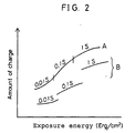
- Fig. 2 is a graph showing the amount of charges on electrostatic information recording medium at a constant light intensity but at varied voltage shutter times, say, 0.01 second, 0.1 second and 1 second.
- the amount of charges corresponds to the quantity of exposure even at varied voltage shutter times, as can be seen from a characteristic curve A.
- the use of the organic photosensitive material results in a phenomenon that even at the same amount of exposure, there is a difference in the quantity of charges between the voltage shutter times 0.01 second and 0.1 second, and 0.1 second and 1 second, as can be seen from characteristic curves B.
- the organic photosensitive material has a low carrier mobility; the carriers generated by exposure disappear, since the voltage is cut off before they reach the charge-carrying medium. Thus, there is a problem that even at the same quantity of exposure, the image potential varies with a voltage shutter time.
- the photosensitive member, gap and electrostatic information recording medium are all considered to be capacitors, each of given capacitance, and if the photosensitive member and electrostatic information recording medium have the same thickness, dielectric constant and area, then both will have an equal electrostatic capacitance. Also, given a gap of about 12-13 ⁇ m between the photosensitive member and the electrostatic information recording medium, then the discharge voltage in the gap will be on the order of about 400V. For instance, now assume that the exposure with the application of voltage is carried out at an application voltage of 2000V. Then, the photosensitive member is made electrically conductive at the region exposed to light. Consequently, the overall "image exposure" system may be considered as an equivalent circuit in which, as illustrated in Fig.
- the unexposed region may be taken as an equivalent circuit in which, as shown in Fig. 4b, 800V, 400V and 800V are applied to the capacitances C1, C2 and C3 of the photosensitive member, gap and electrostatic information recording medium, respectively.
- Fig. 6 is a diagrammatical sketch for illustrating a typical process, so far proposed, for recording electrostatic images with the use of a spacer.
- a photosensitive member 2 - in which a transparent electrode layer 2b and a photoconductive layer 2c are successively laminated on the overall surface of a transparent substrate 2a - is located in opposite relation to electrostatic information recording medium 1 - in which an electrode layer 1b and an insulating layer 1a are successively laminated on the overall surface of a substrate 1c - with a spacer 3 interposed therebetween. With voltage applied between both the electrode layers, the image exposure is carried out through, e.g. the photosensitive member 2.
- the photoconductive layer 2c generates carriers at the exposed region and is made so electrically conductive there that discharge can take place at the exposed region between the photosensitive member and the electrostatic information recording medium, accumulating charges corresponding to the quantity of exposure on the insulating layer 1a and so forming an electrostatic latent image.
- electrode layers are provided on the overall surfaces of the photoconductive material and electrostatic information recording medium with a spacer formed as of an insulating PET film provided between them to keep a discharge gap constant.
- One object of this invention is to obtain the amount of charges corresponding to the exposure energy irrespective of a voltage shutter time, even when an organic photosensitive member is used.
- the photoconductive layer formed of an organic photosensitive member generates carriers upon exposed to light with the application of voltage, but they are so low in terms of mobility that when the voltage is put off, they disappear before reaching the electrostatic information recording medium.
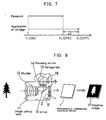
- Fig. 8 is a diagrammatical sketch showing an example of the electrostatic camera making use of the exposure with the application of voltage, wherein the same parts as in Fig. 1 are indicated by the same reference numerals, and other reference numerals represent the following elements: 11 - an image pickup lens, 12 - a mirror, 13 - a shutter, 14 - a focusing screen, 15 - a pentaprism, 16 - an eyepiece, 17 - a negative image and E - a power source.
- the photosensitive member 2 and electrostatic information recording medium 1, shown in Fig. 1 are used in place of a single-lens reflex camera's film.
- a switch (not shown) operated to put on the power source E, voltage is applied to the photosensitive member and electrostatic information recording medium and the shutter 13 is released by a preset time to swing the mirror 12 up to the position shown by a dotted line, forming the electrostatic latent image of a subject on electrostatic information recording medium 1.
- the voltage applied between the photosensitive member and the electrostatic information recording medium is put off.
- the electrostatic information recording medium may then be toner-developed to obtain a negative image 17. It may also be possible to produce electrical signals by reading the electrostatic potential for CRT display or transfer to other recording means such as a magnetic tape.
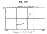
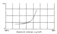
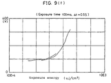
- the photosensitive member and the electrostatic information recording medium were made of an organic photosensitive film of 10 ⁇ m in thickness and a fluoropolymer film of 3 ⁇ m in thickness, respectively, which were located in opposite relation to each other through a gap of 10 ⁇ m. While the photosensitive member was kept positively, a voltage of 750V was applied between the electrodes thereof.
- the light source used was a tungsten lamp having a color temperature of 3000°K.
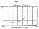
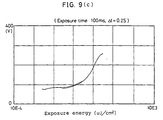
- FIG. 9a A comparison of Fig. 9a with Fig. 9b indicates that in spite of the photosensitive member being exposed to the same light energy, the potential recorded on the electrostatic information recording medium is much larger in Fig. 9b than in Fig. 9a in which the voltage pulse is synchronized with the optical shutter; this reveals that Fig. 9b in which the application of voltage is continued even after the closing of the optical shutter is much more effective than Fig. 9a.
Landscapes
- Physics & Mathematics (AREA)
- General Physics & Mathematics (AREA)
- Electrophotography Using Other Than Carlson'S Method (AREA)
- Photoreceptors In Electrophotography (AREA)
Claims (1)
- Bildaufzeichnungsprozess, bei dem ein lichtempfindliches Bauteil (2), umfassend eine über eine Elektrodenschicht (2b) auf einem Träger (2a) angeordnete unter Lichteinfluss leitende Schicht (2c) einem elektrostatischen Informationsaufzeichnungsmedium (1) gegenüberliegend angeordnet wird, umfassend eine über eine Elektrodenschicht (1b) auf einem Träger (1c) angeordnete Isolierschicht (1a), wobei eine Bildbelichtung stattfindet, wenn eine Spannung an die Elektrodenschichten (2b, 1b) des lichtempfindlichen Bauteils (2) und des Informationsaufzeichnungsmediums (1) angelegt wird, um Ladungen auf dem Informationsaufzeichnungsmedium in bildhafter Form anzusammeln, dadurch gekennzeichnet, dass die Bildbelichtung abgeschaltet wird, gefolgt vom Abschalten der an die Elektrodenschichten angelegten Spannung nach dem Verstreichen eines vorgegebenen Zeitraums.
Applications Claiming Priority (19)
| Application Number | Priority Date | Filing Date | Title |
|---|---|---|---|
| JP29839189 | 1989-11-16 | ||
| JP298391/89 | 1989-11-16 | ||
| JP29839189 | 1989-11-16 | ||
| JP33307889A JP2862299B2 (ja) | 1989-12-22 | 1989-12-22 | 画像記録方法 |
| JP333078/89 | 1989-12-22 | ||
| JP33307889 | 1989-12-22 | ||
| JP1342248A JP2862608B2 (ja) | 1989-12-28 | 1989-12-28 | 画像形成方法および装置 |
| JP342248/89 | 1989-12-28 | ||
| JP34224889 | 1989-12-28 | ||
| JP18602290A JPH0470872A (ja) | 1990-07-12 | 1990-07-12 | スペーサ一体型電荷保持媒体及びその製造方法 |
| JP186021/90 | 1990-07-12 | ||
| JP186023/90 | 1990-07-12 | ||
| JP186022/90 | 1990-07-12 | ||
| JP18602390 | 1990-07-12 | ||
| JP18602190A JPH0470841A (ja) | 1990-07-12 | 1990-07-12 | スペーサ一体型感光体 |
| JP18602390A JP2966055B2 (ja) | 1990-07-12 | 1990-07-12 | 静電画像記録装置 |
| JP18602190 | 1990-07-12 | ||
| JP18602290 | 1990-07-12 | ||
| EP90916801A EP0456827B1 (de) | 1989-11-16 | 1990-11-16 | Verfahren und gerät zur aufzeichnung von bildern |
Related Parent Applications (2)
| Application Number | Title | Priority Date | Filing Date |
|---|---|---|---|
| EP90916801A Division EP0456827B1 (de) | 1989-11-16 | 1990-11-16 | Verfahren und gerät zur aufzeichnung von bildern |
| EP90916801.5 Division | 1990-11-16 |
Publications (3)
| Publication Number | Publication Date |
|---|---|
| EP0697635A2 EP0697635A2 (de) | 1996-02-21 |
| EP0697635A3 EP0697635A3 (de) | 1997-01-15 |
| EP0697635B1 true EP0697635B1 (de) | 2002-02-20 |
Family
ID=27553582
Family Applications (2)
| Application Number | Title | Priority Date | Filing Date |
|---|---|---|---|
| EP95202867A Expired - Lifetime EP0697635B1 (de) | 1989-11-16 | 1990-11-16 | Bildaufzeichnungsprozess |
| EP90916801A Expired - Lifetime EP0456827B1 (de) | 1989-11-16 | 1990-11-16 | Verfahren und gerät zur aufzeichnung von bildern |
Family Applications After (1)
| Application Number | Title | Priority Date | Filing Date |
|---|---|---|---|
| EP90916801A Expired - Lifetime EP0456827B1 (de) | 1989-11-16 | 1990-11-16 | Verfahren und gerät zur aufzeichnung von bildern |
Country Status (4)
| Country | Link |
|---|---|
| US (1) | US5298947A (de) |
| EP (2) | EP0697635B1 (de) |
| DE (2) | DE69033918T2 (de) |
| WO (1) | WO1991007702A1 (de) |
Families Citing this family (8)
| Publication number | Priority date | Publication date | Assignee | Title |
|---|---|---|---|---|
| US5414496A (en) * | 1989-09-21 | 1995-05-09 | Dai Nippon Printing Co., Ltd. | Method for manufacturing a printing plate using a charge carrier medium and method for page make-up using a charge carrier medium |
| US5450168A (en) * | 1990-06-06 | 1995-09-12 | Dai Nippon Printing Co., Ltd. | Moving image pickup device, medium for picking up moving images and process for picking up images continuously |
| JPH04345131A (ja) * | 1991-05-22 | 1992-12-01 | Victor Co Of Japan Ltd | 情報記録装置 |
| EP0595255B1 (de) * | 1992-10-26 | 2001-03-28 | Dai Nippon Printing Co., Ltd. | Photoelektrischer Sensor, Informationsaufzeichnungssystem und Methode zur Informationsaufzeichnung |
| US6094544A (en) * | 1995-02-21 | 2000-07-25 | Asahi Kogaku Kogyo Kabushiki Kaisha | Photographing operation control device |
| JP3238612B2 (ja) * | 1995-03-13 | 2001-12-17 | 旭光学工業株式会社 | 電子現像型カメラの撮像動作制御装置 |
| US5978610A (en) * | 1995-03-14 | 1999-11-02 | Asahi Kogaku Kogyo Kabushiki Kaisha | Exposure control apparatus for electronic development type camera |
| US5655170A (en) * | 1995-06-26 | 1997-08-05 | Asahi Kogaku Kogyo Kabushiki Kaisha | Electro-developing type camera using electro-developing recording medium |
Family Cites Families (22)
| Publication number | Priority date | Publication date | Assignee | Title |
|---|---|---|---|---|
| US2833648A (en) * | 1953-07-16 | 1958-05-06 | Haloid Co | Transfer of electrostatic charge pattern |
| US3598579A (en) * | 1967-09-06 | 1971-08-10 | Eastman Kodak Co | Method of transferring electrostatic images to a dielectric sheet wherein a reversal of potential is used to clear background areas |
| US3653890A (en) * | 1967-10-25 | 1972-04-04 | Konishiroku Photo Ind | Screen electrophotographic charge induction process |
| JPS4910703B1 (de) * | 1969-07-11 | 1974-03-12 | ||
| CH544909A (de) * | 1970-06-06 | 1973-11-30 | Nahr Helmar | Aus mindestens zwei Teilkörpern zusammengesetzter Körper und Verfahren zu seiner Herstellung |
| JPS53103B2 (de) * | 1971-09-07 | 1978-01-05 | ||
| JPS4911584A (de) * | 1972-06-01 | 1974-02-01 | ||
| JPS49107038A (de) * | 1973-02-12 | 1974-10-11 | ||
| US3963488A (en) * | 1974-09-03 | 1976-06-15 | Gaf Corporation | Contrast of electrostatic latent images with a light flooding step |
| US4023895A (en) * | 1974-10-25 | 1977-05-17 | Xerox Corporation | Electrostatographic apparatus |
| US4050804A (en) * | 1976-06-04 | 1977-09-27 | Xerox Corporation | Liquid ink imaging system |
| JPS6016630B2 (ja) * | 1976-11-27 | 1985-04-26 | 日本電気株式会社 | 電子写真装置 |
| JPS52142841U (de) * | 1977-04-22 | 1977-10-29 | ||
| JPS53139537A (en) * | 1977-05-12 | 1978-12-05 | Teijin Ltd | Method of making electrostatic latent image |
| JPS54115139A (en) * | 1978-02-27 | 1979-09-07 | Nec Corp | Electrophotographic apparatus |
| US4628017A (en) * | 1984-11-02 | 1986-12-09 | Ricoh Company, Limited | Electrostatic image forming method |
| JPS61110165A (ja) * | 1984-11-02 | 1986-05-28 | Ricoh Co Ltd | 静電像形成方法 |
| US5161233A (en) * | 1988-05-17 | 1992-11-03 | Dai Nippon Printing Co., Ltd. | Method for recording and reproducing information, apparatus therefor and recording medium |
| US5099261A (en) * | 1988-05-10 | 1992-03-24 | Victor Company Of Japan, Ltd. | Apparatus for recording and reproducing charge latent image |
| EP1033706B1 (de) * | 1988-05-17 | 2004-03-03 | Dai Nippon Printing Co., Ltd. | Elektrostatisches Informationsaufzeichnungsmedium und elektrostatische Informationsaufzeichnungs- und -wiedergabemethode |
| DE69027398T2 (de) * | 1989-03-16 | 1997-01-30 | Dainippon Printing Co Ltd | Bildaufzeichnungsverfahren |
| JP3373900B2 (ja) * | 1993-08-03 | 2003-02-04 | 住友ゴム工業株式会社 | 空気入りタイヤ |
-
1990
- 1990-11-16 WO PCT/JP1990/001497 patent/WO1991007702A1/ja not_active Ceased
- 1990-11-16 DE DE69033918T patent/DE69033918T2/de not_active Expired - Fee Related
- 1990-11-16 DE DE69027427T patent/DE69027427T2/de not_active Expired - Fee Related
- 1990-11-16 EP EP95202867A patent/EP0697635B1/de not_active Expired - Lifetime
- 1990-11-16 US US07/720,858 patent/US5298947A/en not_active Expired - Fee Related
- 1990-11-16 EP EP90916801A patent/EP0456827B1/de not_active Expired - Lifetime
Also Published As
| Publication number | Publication date |
|---|---|
| DE69033918D1 (de) | 2002-03-28 |
| DE69027427T2 (de) | 1997-01-09 |
| DE69033918T2 (de) | 2002-11-28 |
| WO1991007702A1 (fr) | 1991-05-30 |
| DE69027427D1 (de) | 1996-07-18 |
| EP0697635A3 (de) | 1997-01-15 |
| EP0697635A2 (de) | 1996-02-21 |
| EP0456827A1 (de) | 1991-11-21 |
| EP0456827A4 (en) | 1993-09-08 |
| US5298947A (en) | 1994-03-29 |
| EP0456827B1 (de) | 1996-06-12 |
Similar Documents
| Publication | Publication Date | Title |
|---|---|---|
| US3752572A (en) | Apparatus for making electrographs | |
| US3676117A (en) | Method of electrophotography | |
| US3653064A (en) | Electrostatic image-forming apparatus and process | |
| US4170475A (en) | High speed electrophotographic method | |
| US3185051A (en) | Xerographic method | |
| EP0697635B1 (de) | Bildaufzeichnungsprozess | |
| US4207100A (en) | Formation of electrostatic latent image | |
| US3655369A (en) | Persistent internal polarization process in electrophotography | |
| US4757343A (en) | Electrostatic image output apparatus | |
| US4242433A (en) | High speed electrophotographic medium | |
| US4197119A (en) | Electrophotographic process | |
| CA1174889A (en) | Imaging member including an intermediate layer of an acetal of poly(vinyl alcohol) and a photoconductive layer | |
| JP3031694B2 (ja) | 電圧印加露光方法 | |
| US3761951A (en) | Electrostatic image forming apparatus | |
| US3837853A (en) | Electrophotographic method of imaging with an element containing an amorphous semiconductor | |
| US3781108A (en) | Method and apparatus for forming latent electrostatic images | |
| US3843361A (en) | Electrophotography using induced electrostatic images | |
| US4155640A (en) | High speed electrophotographic imaging system | |
| JP2826119B2 (ja) | 光電子倍増効果を有する感光体、及び静電画像記録方法 | |
| JP2692892B2 (ja) | 電圧印加露光方法 | |
| JP2862299B2 (ja) | 画像記録方法 | |
| JP2835368B2 (ja) | 画像形成方法及び画像形成装置 | |
| US3700436A (en) | Electrode configuration for electrophotography | |
| SU1097966A1 (ru) | Способ формировани скрытого электростатического изображени на электрофотографическом носителе с диэлектрическим покрытием | |
| JP3465097B2 (ja) | 潜像転写用電子写真感光体 |
Legal Events
| Date | Code | Title | Description |
|---|---|---|---|
| PUAI | Public reference made under article 153(3) epc to a published international application that has entered the european phase |
Free format text: ORIGINAL CODE: 0009012 |
|
| AC | Divisional application: reference to earlier application |
Ref document number: 456827 Country of ref document: EP |
|
| AK | Designated contracting states |
Kind code of ref document: A2 Designated state(s): DE FR GB IT |
|
| PUAL | Search report despatched |
Free format text: ORIGINAL CODE: 0009013 |
|
| AK | Designated contracting states |
Kind code of ref document: A3 Designated state(s): DE FR GB IT |
|
| 17P | Request for examination filed |
Effective date: 19970709 |
|
| 17Q | First examination report despatched |
Effective date: 19990316 |
|
| RTI1 | Title (correction) |
Free format text: PROCESS FOR RECORDING IMAGES |
|
| GRAG | Despatch of communication of intention to grant |
Free format text: ORIGINAL CODE: EPIDOS AGRA |
|
| GRAG | Despatch of communication of intention to grant |
Free format text: ORIGINAL CODE: EPIDOS AGRA |
|
| GRAH | Despatch of communication of intention to grant a patent |
Free format text: ORIGINAL CODE: EPIDOS IGRA |
|
| GRAH | Despatch of communication of intention to grant a patent |
Free format text: ORIGINAL CODE: EPIDOS IGRA |
|
| REG | Reference to a national code |
Ref country code: GB Ref legal event code: IF02 |
|
| GRAA | (expected) grant |
Free format text: ORIGINAL CODE: 0009210 |
|
| AC | Divisional application: reference to earlier application |
Ref document number: 456827 Country of ref document: EP |
|
| AK | Designated contracting states |
Kind code of ref document: B1 Designated state(s): DE FR GB IT |
|
| REF | Corresponds to: |
Ref document number: 69033918 Country of ref document: DE Date of ref document: 20020328 |
|
| ET | Fr: translation filed | ||
| PLBE | No opposition filed within time limit |
Free format text: ORIGINAL CODE: 0009261 |
|
| STAA | Information on the status of an ep patent application or granted ep patent |
Free format text: STATUS: NO OPPOSITION FILED WITHIN TIME LIMIT |
|
| 26N | No opposition filed |
Effective date: 20021121 |
|
| PG25 | Lapsed in a contracting state [announced via postgrant information from national office to epo] |
Ref country code: DE Free format text: LAPSE BECAUSE OF NON-PAYMENT OF DUE FEES Effective date: 20030603 |
|
| PGFP | Annual fee paid to national office [announced via postgrant information from national office to epo] |
Ref country code: GB Payment date: 20031104 Year of fee payment: 14 |
|
| PGFP | Annual fee paid to national office [announced via postgrant information from national office to epo] |
Ref country code: FR Payment date: 20031106 Year of fee payment: 14 |
|
| PG25 | Lapsed in a contracting state [announced via postgrant information from national office to epo] |
Ref country code: GB Free format text: LAPSE BECAUSE OF NON-PAYMENT OF DUE FEES Effective date: 20041116 |
|
| GBPC | Gb: european patent ceased through non-payment of renewal fee |
Effective date: 20041116 |
|
| PG25 | Lapsed in a contracting state [announced via postgrant information from national office to epo] |
Ref country code: FR Free format text: LAPSE BECAUSE OF NON-PAYMENT OF DUE FEES Effective date: 20050729 |
|
| REG | Reference to a national code |
Ref country code: FR Ref legal event code: ST |
|
| PG25 | Lapsed in a contracting state [announced via postgrant information from national office to epo] |
Ref country code: IT Free format text: LAPSE BECAUSE OF NON-PAYMENT OF DUE FEES Effective date: 20051116 |

