EP0694086B1 - Method for planarization of submicron vias and the manufacture of semiconductor integrated circuits - Google Patents
Method for planarization of submicron vias and the manufacture of semiconductor integrated circuits Download PDFInfo
- Publication number
- EP0694086B1 EP0694086B1 EP94912876A EP94912876A EP0694086B1 EP 0694086 B1 EP0694086 B1 EP 0694086B1 EP 94912876 A EP94912876 A EP 94912876A EP 94912876 A EP94912876 A EP 94912876A EP 0694086 B1 EP0694086 B1 EP 0694086B1
- Authority
- EP
- European Patent Office
- Prior art keywords
- temperature
- substrate
- vias
- conductor
- layer
- Prior art date
- Legal status (The legal status is an assumption and is not a legal conclusion. Google has not performed a legal analysis and makes no representation as to the accuracy of the status listed.)
- Expired - Lifetime
Links
Images

Classifications
-
- H10W20/059—
-
- C—CHEMISTRY; METALLURGY
- C23—COATING METALLIC MATERIAL; COATING MATERIAL WITH METALLIC MATERIAL; CHEMICAL SURFACE TREATMENT; DIFFUSION TREATMENT OF METALLIC MATERIAL; COATING BY VACUUM EVAPORATION, BY SPUTTERING, BY ION IMPLANTATION OR BY CHEMICAL VAPOUR DEPOSITION, IN GENERAL; INHIBITING CORROSION OF METALLIC MATERIAL OR INCRUSTATION IN GENERAL
- C23C—COATING METALLIC MATERIAL; COATING MATERIAL WITH METALLIC MATERIAL; SURFACE TREATMENT OF METALLIC MATERIAL BY DIFFUSION INTO THE SURFACE, BY CHEMICAL CONVERSION OR SUBSTITUTION; COATING BY VACUUM EVAPORATION, BY SPUTTERING, BY ION IMPLANTATION OR BY CHEMICAL VAPOUR DEPOSITION, IN GENERAL
- C23C14/00—Coating by vacuum evaporation, by sputtering or by ion implantation of the coating forming material
- C23C14/04—Coating on selected surface areas, e.g. using masks
- C23C14/046—Coating cavities or hollow spaces, e.g. interior of tubes; Infiltration of porous substrates
-
- C—CHEMISTRY; METALLURGY
- C23—COATING METALLIC MATERIAL; COATING MATERIAL WITH METALLIC MATERIAL; CHEMICAL SURFACE TREATMENT; DIFFUSION TREATMENT OF METALLIC MATERIAL; COATING BY VACUUM EVAPORATION, BY SPUTTERING, BY ION IMPLANTATION OR BY CHEMICAL VAPOUR DEPOSITION, IN GENERAL; INHIBITING CORROSION OF METALLIC MATERIAL OR INCRUSTATION IN GENERAL
- C23C—COATING METALLIC MATERIAL; COATING MATERIAL WITH METALLIC MATERIAL; SURFACE TREATMENT OF METALLIC MATERIAL BY DIFFUSION INTO THE SURFACE, BY CHEMICAL CONVERSION OR SUBSTITUTION; COATING BY VACUUM EVAPORATION, BY SPUTTERING, BY ION IMPLANTATION OR BY CHEMICAL VAPOUR DEPOSITION, IN GENERAL
- C23C14/00—Coating by vacuum evaporation, by sputtering or by ion implantation of the coating forming material
- C23C14/06—Coating by vacuum evaporation, by sputtering or by ion implantation of the coating forming material characterised by the coating material
- C23C14/14—Metallic material, boron or silicon
- C23C14/18—Metallic material, boron or silicon on other inorganic substrates
- C23C14/185—Metallic material, boron or silicon on other inorganic substrates by cathodic sputtering
-
- C—CHEMISTRY; METALLURGY
- C23—COATING METALLIC MATERIAL; COATING MATERIAL WITH METALLIC MATERIAL; CHEMICAL SURFACE TREATMENT; DIFFUSION TREATMENT OF METALLIC MATERIAL; COATING BY VACUUM EVAPORATION, BY SPUTTERING, BY ION IMPLANTATION OR BY CHEMICAL VAPOUR DEPOSITION, IN GENERAL; INHIBITING CORROSION OF METALLIC MATERIAL OR INCRUSTATION IN GENERAL
- C23C—COATING METALLIC MATERIAL; COATING MATERIAL WITH METALLIC MATERIAL; SURFACE TREATMENT OF METALLIC MATERIAL BY DIFFUSION INTO THE SURFACE, BY CHEMICAL CONVERSION OR SUBSTITUTION; COATING BY VACUUM EVAPORATION, BY SPUTTERING, BY ION IMPLANTATION OR BY CHEMICAL VAPOUR DEPOSITION, IN GENERAL
- C23C14/00—Coating by vacuum evaporation, by sputtering or by ion implantation of the coating forming material
- C23C14/22—Coating by vacuum evaporation, by sputtering or by ion implantation of the coating forming material characterised by the process of coating
- C23C14/34—Sputtering
- C23C14/3492—Variation of parameters during sputtering
-
- C—CHEMISTRY; METALLURGY
- C23—COATING METALLIC MATERIAL; COATING MATERIAL WITH METALLIC MATERIAL; CHEMICAL SURFACE TREATMENT; DIFFUSION TREATMENT OF METALLIC MATERIAL; COATING BY VACUUM EVAPORATION, BY SPUTTERING, BY ION IMPLANTATION OR BY CHEMICAL VAPOUR DEPOSITION, IN GENERAL; INHIBITING CORROSION OF METALLIC MATERIAL OR INCRUSTATION IN GENERAL
- C23C—COATING METALLIC MATERIAL; COATING MATERIAL WITH METALLIC MATERIAL; SURFACE TREATMENT OF METALLIC MATERIAL BY DIFFUSION INTO THE SURFACE, BY CHEMICAL CONVERSION OR SUBSTITUTION; COATING BY VACUUM EVAPORATION, BY SPUTTERING, BY ION IMPLANTATION OR BY CHEMICAL VAPOUR DEPOSITION, IN GENERAL
- C23C14/00—Coating by vacuum evaporation, by sputtering or by ion implantation of the coating forming material
- C23C14/22—Coating by vacuum evaporation, by sputtering or by ion implantation of the coating forming material characterised by the process of coating
- C23C14/54—Controlling or regulating the coating process
- C23C14/541—Heating or cooling of the substrates
-
- H10P95/04—
Definitions
- the active switching elements of integrated circuits are interconnected by metal lines deposited by various methods such as physical vapor deposition, chemical vapor deposition and evaporation. Typically, several levels of metal lines are used in an integrated circuit to allow crossovers. At certain locations, electrical contact is made between lines of different levels. Such locations are called vias.
- the most commonly used interconnecting metal for high aspect ratio vias is the tungsten plug deposited by the decomposition of tungsten hexafluoride on the sidewall of the via.
- Such plugs are formed by either selective deposition which has not been reliable enough to be used for manufacturing purposes or by the blanket deposition of a film with successive etch back. All tungsten depositions require the prior deposition of an adhesive layer which is typically a layer of plasma vapor deposited titanium nitride.
- the titanium nitride deposition may result in a re-entrant profile particularly on geometries with high aspect ratios.
- the resulting chemical vapor deposition then shows the well known keyhole which results in integrated circuit reliability problems and limits the use of tungsten chemical vapor deposition to critical geometries of greater than .5 microns.
- tungsten chemical vapor deposition processes are complex and expensive. Due to the high resistivity of tungsten, material contact resistances and via resistance are high and can limit the performance of integrated circuits.
- This process requires a continuous diffusion path along the sidewall of the via and is dependent on achieving certain process conditions simultaneously. These conditions are sometimes difficult to achieve and control.
- Tracy U.S. Patent 4,970,176 discloses deposition of a relatively thick layer of aluminum at a first temperature and a subsequent deposition of a thin layer of aluminum at a higher temperature.
- the specification indicates that the temperature increase acts to reflow the aluminum through grain growth and recrystallization.
- the filling of the via starts from the bottom of the via and works up to the top.
- the Tracy application was filed, typically the vias were of a size greater than one micron.
- a method of filling a via in a substrate comprising depositing a layer of a metal conductor having a coefficient of thermal expansion onto the substrate at a first temperature wherein the layer covers the vias and wherein the substrate has a lower coefficient of thermal expansion than the metal conductor, and heating the substrate and the deposited conductor to a second temperature, characterised in that the method is for filling a submicron vias; in that the layer of metal conductor when deposited leaves a void space in the vias below the layer and in that the layer of the deposited metal conductor is effectively thick so that thermal stress created by increasing the temperature from the first temperature to the second temperature and the relative coefficient of thermal expansions of the conductor and the substrate cause the conductor to expand and uniformly fill the void in the submicron vias.
- the present invention is premised on the realization that submicron vias can be effectively and reliably filled by sputter deposition of aluminum.
- the present invention utilizes via filling by extrusion.
- aluminum is sputter deposited over a via at a first temperature. It is then put into compression by the addition of thermal energy. When the film is heated sufficiently, and assuming an effectively thick initial aluminum deposition, it will plasticly deform and be forced into the via. The temperature of plastic deformation is characteristic
- the present invention is a method of filling vias, particularly those having submicron diameters, where the aspect ratio of the via, that is the height to diameter ratio is from about 1 to about 4.
- aluminum will be deposited into vias having diameters from 0.7 to about 0.1 ⁇ m preferably 0.5 to 0.25 ⁇ m.
- a substrate which includes one or more vias is initially coated with an aluminum or aluminum alloy layer.
- the aluminum layer is put into compression by increasing the wafer temperature. The difference in coefficients of thermal expansion between the substrate and the aluminum forces the aluminum into compression. The compressive force will cause the aluminum to flow into and fill the via.
- the substrates for use in the present invention will include silicon layers, boron and phosphorus doped silica, thermal oxide and TEOS oxide.
- the coefficients of thermal expansion of these materials is shown in Table 1. Silicon 3.24 [ppm /°C] [10 -6 /K] Boron and Phosphorus doped silica 0.5-0.6 [ppm/ ° C] [10 -6 /K] Quartz 0.55 [ppm /°C] [10 -6 /K] Si 3 Ni 4 1.5-1.6 [ppm/ ° C] [10 -6 /K]
- the thermal expansion co-efficient of most glasses used should be about equal to that of quartz.
- Aluminum or an aluminum alloy is sputter deposited on the substrate.
- aluminum alloys such as Al Si (1%), Al Si (1%)-Cu (0.5%), Al-Cu (1%) and Al-Ti (0.15%) can be used. Due to the high concentration of aluminum, all of these alloys will have a coefficient of thermal expansion of about 24 [ppm/ °c] [10 -6 /K].
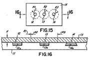
- a substrate 11 having three vias 12, 13, 14 is coated by the aluminum layer 15 having a thickness or height of H.
- the volume 12(a), 13(a) and 14(a) of the vias is shaded.
- Each via has an available radius of aluminum which is approximately equal to one-half the distance to the next adjacent via measure focus to focus. This is shown as Rl, R2, and R3 in Fig. 15.
- Rl, R2, and R3 there is a cylinder of aluminum defined by the radius and thickness H which is equal to 2 ⁇ R 2 H which is available to develop the necessary compressive stress required to extrude the aluminum necessary to fill the volume of the via.
- the temperature After deposition of the aluminum on the wafer, the temperature will be increased. To fill the via, the cylinder times the differential thermal expansion between the substrate and the aluminum layer must be at least equal the volume of the via. Upon heating the deposited aluminum, the increase in volume of the available aluminum caused by the change in temperature should equal the void volume of the via. To completely fill a via having a volume of 0.8 cubic ⁇ m 3 there must be an available radius of 7 ⁇ m if the film thickness is 1 ⁇ m and the temperature change is 100°C. This assumes that the substrate is silicon and the metal is aluminum. If the via to be filled has a volume of only 0.2 ⁇ m 3 , an available radius of 3 ⁇ m for a film thickness of 1 ⁇ m is required. If the temperature rises 200°, then the respective radii are 3.7 ⁇ m and 1.5 ⁇ m, respectively.
- the available radius limits the material available for via filling by extrusion and thus restricts the density of vias this process will support.
- the values shown apply to most, if not, all practical integrated circuits.
- the film thickness of the deposited aluminum can be increased. This increases the amount of material available for filling the via by extrusion and thus reduces the radius proportionally.
- Highly dense arrays of via holes with large volumes can be filled by the deposition of a thicker layer which after the extrusion process can be etched back to nominal thickness.
- the present invention will be conducted in a multichambered sputtering unit which would include an etching chamber and two or more sputtering chambers.
- a multichambered sputtering unit which would include an etching chamber and two or more sputtering chambers.
- One such machine is Eclipse brand sputtering system sold by Materials Research Corporation (also referred to in U.S. Patent 4,994,162). Other commercially available systems are equally suitable.
- the substrate can be initially etched to remove surface impurities. Heating of the substrate also assists in removal of outgases. This is optional but preferred. The substrate is then moved to the second chamber.
- a barrier layer can be applied if desired.
- a preferred barrier is TiN although ZrN and RuO 2 barrier layers can also be used. However, barrier layers may not be required in all applications.
- the thickness of the barrier layer will be about 100 to 200 nm (1000 to about 2000 Angstroms). If the original via sidewalls are normal to the wafer surface, then this establishes a slight inwardly (negative) sloped re-entrant profile at the via. This sloped or undercut re-entrant profile facilitates movement of the aluminum into the via under compression. Basically it decreases the opening so that the initial aluminum layer covers the opening without filling it. The larger the via the thicker the barrier layer and initial aluminum layer should be. But, the opening should not have a radius less than 0.1 ⁇ m. Further, it is preferred to have an inward re-entrant profile of 0 to 20° and preferably 5-10°. The barrier layer assists in forming this.
- the substrate In a third chamber, the substrate is cooled to about room temperature. It is then transferred to a final chamber where the aluminum is deposited.
- a thick layer 2000 to 5000 angstrom (200 to 500 nm) of aluminum initially at a temperature of about 20-50°C. with sputter power of about 3-15 kW.
- a bias voltage may be applied if desired, but is not necessary.
- the substrate and aluminum are subsequently heated to a temperature which forces the aluminum to expand relative to the substrate.
- Figures 1-12 show various vias filled under various parameters to demonstrate successful and failed attempts.
- Fig. 1 shows a closely spaced pattern with apparent voids. This figure of unsuccessful planarization demonstrates two facts that 1) via filling is not through a continuous film along the sidewalls and from the bottom up, but occurs from the top down filling an already existing void, and 2) very high pattern density does not allow sufficient stress to develop to completely fill the via.
- Figs. 2 and 3 show successful planarization in vias spaced further apart.
- the vias in the substrate were filled by initially etching the wafer surface at 500°C. for 120 seconds with argon gas, (50 SCCM), (gas pressure 4.7 millitor) (0.627 N/m 2 ). In addition to surface cleaning, this step is intended to desorb water which may be present in the film.
- the wafer was coated with a TiN barrier coating. With a back plane temperature of 300° C, a 350 angstrom (35 nm) film was applied with 50 SCCM argon gas flow and 2.2 SCCM nitrogen gas flow (applied voltages of 3 kV).
- 20 SCCM of argon was introduced while the back plane gas was maintained and 27 SCCM of nitrogen gas admitted.
- 800 angstroms (80 nm) TiN was applied with a DC power of 6 kV, for 33 seconds. (The argon admitted at 20 SCCM.)
- this wafer was cooled down over 120 seconds with back plane and therefore back plane gas at room temperature.
- the wafer could be actively cooled in this chamber using a refrigerated gas. Rapidly cooling the wafer to 0 + -40°C over 120 seconds can enhance the end product.
- an initial aluminum layer of 2500 angstroms (250 nm) was applied with a DC power of 11.0 kV over 12 seconds with 100 SCCM flow of argon supplied as sputter gas. No back plane gas was admitted. The wafer temperature therefore stayed at approximately 50°C.
- the back plane gas was applied at a temperature of 550°C.
- a 3000 angstrom (300 nm) film of aluminum was deposited. The results are shown in Fig. 2.
- Fig. 3 The results shown in Fig. 3 are obtained in a similar process. Initially the substrate was etched and baked at a temperature of 500°C. The wafer was then coated with a titanium nitride layer approximately 1500 angstroms (150 nm) followed by a cool down step in the third chamber. In the final chamber, a 5000 angstrom (500 nm) aluminum film was applied (over 14 seconds) to the substrate at room temperature (no greater than 50°C,) with a DC power of 11.0 kV. Over the next 43 seconds, 3000 angstroms (300 nm) of aluminum was applied with the back plane gas applied at 550°C.
- a 5000 angstrom (500 nm) aluminum film was applied (over 14 seconds) to the substrate at room temperature (no greater than 50°C,) with a DC power of 11.0 kV.
- 3000 angstroms (300 nm) of aluminum was applied with the back plane gas applied at 550°C.
- the DC power was changed to 3.7 kV and over a period of 36 seconds (100 SCCM of argon gas), the back plane gas was applied at a temperature of 550°C. During this period, 3500 angstroms (350 nm) of aluminum was deposited.
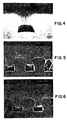
- Fig. 4 shows a pattern in silicon dioxide showing a negative slope (inward) re-entrant angle filled by the method of the present invention. Such a structure is impossible to fill entirely with any of the prior art methods.
- Fig. 5 shows a first unsuccessful attempt to planarize a feature with re-entrant via angle.
- the pattern is of high density and the final temperature reached is 500°C.
- the temperature of the initial cold step is approximately 100° indicating a total temperature rise of 400°C.
- the severity of the pattern, extremely closely spaced, does not allow sufficient stress to develop to effectively fill the via and the via is only half filled.
- Fig. 6, shows a similarly dense pattern with a final temperature of 550°C. (a 450°C. temperature rise).
- the filling of the via from the top has clearly progressed and it appears now approximately 2/3 filled.
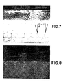
- raising the temperature to 600° thus a temperature differential of 500°C., shows complete via filling even in the highly dense structure shown in Figs.
- the via shown in Fig. 7 has a re-entrant angle of greater than 16° (measured from a line perpendicular to the plane of the substrate) preventing depositing a continuous film along the sidewall. Diffusion along such a sidewall would be disrupted at the film discontinuity and thus impossible using prior art techniques.
- This technology applies for vias with any re-entrant profile. However, generally it is preferred to have a re-entrant profile of 5° to 10'.
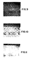
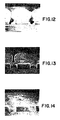
- Figs. 9-11 and 12-14 demonstrate another element of the present invention.
- Figs. 9-11 show via filling of less densely spaced small vias (0.6 ⁇ m) than shown in Figs. 5-7 and thus are able to be planarized at lower temperatures (540°C.). An increasing amount of time for stress release may be required in these situations.
- a hot sputtering time of 50 seconds was employed and a void remained on the very bottom of the via.
- the via shown in Fig. 10 is sputtered for 1 minute and is completely filled.
- sputtering for 2 minutes completely fills the via.
- Figs. 12-14 show larger vias, 0.8 ⁇ m on identical wafers.
- the vias shown in Figs. 9 and 12 were processed under identical conditions, likewise the vias shown in Figs. 10 and 13 and Figs. 11 and 14.
- 50 seconds and 1 minute stress release time are insufficient for complete void free via filling.
- Two minute stress release time completely fills the via.
- Pattern densities in integrated circuit typically are substantially less dense than shown in these test patterns. Therefore allowing the set-up of adequate stress fields at lower temperatures and shorter heat cycle.
- the present invention provides a method to fill vias with sputter deposited aluminum without extreme control of multiple parameters.
- This is widely adaptable, vias having diameters of 0.1 to 0.8 ⁇ m and aspect ratios of 1.0 to 4.0, and having re-entrant profiles from 0° to up to 20°.
Landscapes
- Chemical & Material Sciences (AREA)
- Chemical Kinetics & Catalysis (AREA)
- Engineering & Computer Science (AREA)
- Materials Engineering (AREA)
- Mechanical Engineering (AREA)
- Metallurgy (AREA)
- Organic Chemistry (AREA)
- Inorganic Chemistry (AREA)
- Internal Circuitry In Semiconductor Integrated Circuit Devices (AREA)
- Electrodes Of Semiconductors (AREA)
Applications Claiming Priority (3)
| Application Number | Priority Date | Filing Date | Title |
|---|---|---|---|
| US47265 | 1993-04-13 | ||
| US08/047,265 US5360524A (en) | 1993-04-13 | 1993-04-13 | Method for planarization of submicron vias and the manufacture of semiconductor integrated circuits |
| PCT/US1994/003286 WO1994024330A1 (en) | 1993-04-13 | 1994-03-25 | Method for planarization of submicron vias and the manufacture of semiconductor integrated circuits |
Publications (3)
| Publication Number | Publication Date |
|---|---|
| EP0694086A1 EP0694086A1 (en) | 1996-01-31 |
| EP0694086A4 EP0694086A4 (en) | 1998-03-04 |
| EP0694086B1 true EP0694086B1 (en) | 2001-08-29 |
Family
ID=21947981
Family Applications (1)
| Application Number | Title | Priority Date | Filing Date |
|---|---|---|---|
| EP94912876A Expired - Lifetime EP0694086B1 (en) | 1993-04-13 | 1994-03-25 | Method for planarization of submicron vias and the manufacture of semiconductor integrated circuits |
Country Status (9)
| Country | Link |
|---|---|
| US (1) | US5360524A (enExample) |
| EP (1) | EP0694086B1 (enExample) |
| JP (1) | JP3400454B2 (enExample) |
| KR (1) | KR100308467B1 (enExample) |
| AU (1) | AU6525294A (enExample) |
| CA (1) | CA2159648A1 (enExample) |
| DE (1) | DE69428113T2 (enExample) |
| TW (1) | TW272305B (enExample) |
| WO (1) | WO1994024330A1 (enExample) |
Families Citing this family (15)
| Publication number | Priority date | Publication date | Assignee | Title |
|---|---|---|---|---|
| EP0608628A3 (en) * | 1992-12-25 | 1995-01-18 | Kawasaki Steel Co | Method for manufacturing a semiconductor device with a multilayer connection structure. |
| JP3382031B2 (ja) * | 1993-11-16 | 2003-03-04 | 株式会社東芝 | 半導体装置の製造方法 |
| US5668055A (en) * | 1995-05-05 | 1997-09-16 | Applied Materials, Inc. | Method of filling of contact openings and vias by self-extrusion of overlying compressively stressed matal layer |
| JPH0936230A (ja) * | 1995-05-15 | 1997-02-07 | Sony Corp | 半導体装置の製造方法 |
| JPH09115866A (ja) * | 1995-10-17 | 1997-05-02 | Mitsubishi Electric Corp | 半導体装置の製造方法 |
| US5851920A (en) * | 1996-01-22 | 1998-12-22 | Motorola, Inc. | Method of fabrication of metallization system |
| US5789317A (en) * | 1996-04-12 | 1998-08-04 | Micron Technology, Inc. | Low temperature reflow method for filling high aspect ratio contacts |
| US5891803A (en) * | 1996-06-26 | 1999-04-06 | Intel Corporation | Rapid reflow of conductive layers by directional sputtering for interconnections in integrated circuits |
| US6309971B1 (en) | 1996-08-01 | 2001-10-30 | Cypress Semiconductor Corporation | Hot metallization process |
| EP0867940A3 (en) | 1997-03-27 | 1999-10-13 | Applied Materials, Inc. | An underlayer for an aluminum interconnect |
| US5882399A (en) * | 1997-08-23 | 1999-03-16 | Applied Materials, Inc. | Method of forming a barrier layer which enables a consistently highly oriented crystalline structure in a metallic interconnect |
| FR2769923B1 (fr) * | 1997-10-17 | 2001-12-28 | Cypress Semiconductor Corp | Procede ameliore de metallisation a chaud |
| US6965165B2 (en) * | 1998-12-21 | 2005-11-15 | Mou-Shiung Lin | Top layers of metal for high performance IC's |
| US7381642B2 (en) | 2004-09-23 | 2008-06-03 | Megica Corporation | Top layers of metal for integrated circuits |
| US7405149B1 (en) * | 1998-12-21 | 2008-07-29 | Megica Corporation | Post passivation method for semiconductor chip or wafer |
Family Cites Families (10)
| Publication number | Priority date | Publication date | Assignee | Title |
|---|---|---|---|---|
| US4661228A (en) * | 1984-05-17 | 1987-04-28 | Varian Associates, Inc. | Apparatus and method for manufacturing planarized aluminum films |
| US4865712A (en) * | 1984-05-17 | 1989-09-12 | Varian Associates, Inc. | Apparatus for manufacturing planarized aluminum films |
| US4657628A (en) * | 1985-05-01 | 1987-04-14 | Texas Instruments Incorporated | Process for patterning local interconnects |
| EP0544648B1 (en) * | 1985-05-13 | 1997-04-09 | Nippon Telegraph And Telephone Corporation | Method for forming a planarized Al thin film |
| JPS63162854A (ja) * | 1986-12-25 | 1988-07-06 | Fujitsu Ltd | 金属膜形成方法 |
| US4994162A (en) * | 1989-09-29 | 1991-02-19 | Materials Research Corporation | Planarization method |
| US4970176A (en) * | 1989-09-29 | 1990-11-13 | Motorola, Inc. | Multiple step metallization process |
| US5108570A (en) * | 1990-03-30 | 1992-04-28 | Applied Materials, Inc. | Multistep sputtering process for forming aluminum layer over stepped semiconductor wafer |
| KR920010620A (ko) * | 1990-11-30 | 1992-06-26 | 원본미기재 | 다층 상호접속선을 위한 알루미늄 적층 접점/통로 형성방법 |
| JPH07109030B2 (ja) * | 1991-02-12 | 1995-11-22 | アプライド マテリアルズ インコーポレイテッド | 半導体ウェーハ上にアルミニウム層をスパッタする方法 |
-
1993
- 1993-04-13 US US08/047,265 patent/US5360524A/en not_active Expired - Lifetime
-
1994
- 1994-03-21 TW TW083102461A patent/TW272305B/zh not_active IP Right Cessation
- 1994-03-25 AU AU65252/94A patent/AU6525294A/en not_active Abandoned
- 1994-03-25 CA CA002159648A patent/CA2159648A1/en not_active Abandoned
- 1994-03-25 DE DE69428113T patent/DE69428113T2/de not_active Expired - Lifetime
- 1994-03-25 EP EP94912876A patent/EP0694086B1/en not_active Expired - Lifetime
- 1994-03-25 JP JP52320794A patent/JP3400454B2/ja not_active Expired - Lifetime
- 1994-03-25 KR KR1019950704442A patent/KR100308467B1/ko not_active Expired - Lifetime
- 1994-03-25 WO PCT/US1994/003286 patent/WO1994024330A1/en not_active Ceased
Also Published As
| Publication number | Publication date |
|---|---|
| KR100308467B1 (ko) | 2001-11-30 |
| EP0694086A4 (en) | 1998-03-04 |
| US5360524A (en) | 1994-11-01 |
| DE69428113T2 (de) | 2002-01-24 |
| JPH08509101A (ja) | 1996-09-24 |
| DE69428113D1 (de) | 2001-10-04 |
| EP0694086A1 (en) | 1996-01-31 |
| KR960702014A (ko) | 1996-03-28 |
| CA2159648A1 (en) | 1994-10-27 |
| WO1994024330A1 (en) | 1994-10-27 |
| TW272305B (enExample) | 1996-03-11 |
| JP3400454B2 (ja) | 2003-04-28 |
| AU6525294A (en) | 1994-11-08 |
Similar Documents
| Publication | Publication Date | Title |
|---|---|---|
| EP0694086B1 (en) | Method for planarization of submicron vias and the manufacture of semiconductor integrated circuits | |
| KR100291284B1 (ko) | 알루미늄금속층배선방법 | |
| US6090701A (en) | Method for production of semiconductor device | |
| US5371042A (en) | Method of filling contacts in semiconductor devices | |
| HK167395A (en) | Integrated semiconductor circuit with at least two planes made of aluminium or aluminium compound and method of manufacturing the same | |
| US5847461A (en) | Integrated circuit structure having contact openings and vias filled by self-extrusion of overlying metal layer | |
| EP0954015B1 (en) | High throughput Al-Cu thin film sputtering process on small contact via | |
| EP0478871B1 (en) | Formation of contact plugs by blanket CVD deposition and etchback | |
| US6486559B1 (en) | Copper wiring structure comprising a copper material buried in a hollow of an insulating film and a carbon layer between the hollow and the copper material in semiconductor device and method of fabricating the same | |
| KR20010034151A (ko) | 금속화 방법 및 장치 | |
| KR19990063873A (ko) | 집적 회로용 금속 스택의 티타늄과 알루미늄 합금사이의 개선된 인터페이스 | |
| EP0840370B1 (en) | Low temperature aluminum reflow for multilevel metallization | |
| EP0740336A2 (en) | Method for fabricating semiconductor device having buried contact structure | |
| US5702983A (en) | Method for manufacturing a semiconductor device with a metallic interconnection layer | |
| US6200894B1 (en) | Method for enhancing aluminum interconnect properties | |
| US20030170975A1 (en) | Method for forming a metal extrusion free via | |
| KR100213447B1 (ko) | 반도체 소자의 금속 배선 형성방법 | |
| US6982226B1 (en) | Method of fabricating a contact with a post contact plug anneal | |
| EP0852809A1 (en) | Metal stack for integrated circuit having two thin layers of titanium with dedicated chamber depositions | |
| US20030124828A1 (en) | System for improving thermal stability of copper damascene structure | |
| JP2928057B2 (ja) | 半導体装置の製造方法 | |
| JP2586292B2 (ja) | 半導体装置の製造方法 | |
| CN1146021C (zh) | 具有多层布线的半导体器件的制造方法 | |
| Depinto et al. | Effects of aluminum sputtering process parameters on via step coverage in micro-electronic device manufacturing | |
| JPH05160083A (ja) | 絶縁膜の平坦化方法 |
Legal Events
| Date | Code | Title | Description |
|---|---|---|---|
| PUAI | Public reference made under article 153(3) epc to a published international application that has entered the european phase |
Free format text: ORIGINAL CODE: 0009012 |
|
| 17P | Request for examination filed |
Effective date: 19951002 |
|
| AK | Designated contracting states |
Kind code of ref document: A1 Designated state(s): BE CH DE FR GB IT LI LU NL SE |
|
| A4 | Supplementary search report drawn up and despatched |
Effective date: 19980119 |
|
| AK | Designated contracting states |
Kind code of ref document: A4 Designated state(s): BE CH DE FR GB IT LI LU NL SE |
|
| RAP1 | Party data changed (applicant data changed or rights of an application transferred) |
Owner name: TOKYO ELECTRON LIMITED |
|
| 17Q | First examination report despatched |
Effective date: 19990201 |
|
| GRAG | Despatch of communication of intention to grant |
Free format text: ORIGINAL CODE: EPIDOS AGRA |
|
| GRAG | Despatch of communication of intention to grant |
Free format text: ORIGINAL CODE: EPIDOS AGRA |
|
| GRAH | Despatch of communication of intention to grant a patent |
Free format text: ORIGINAL CODE: EPIDOS IGRA |
|
| GRAH | Despatch of communication of intention to grant a patent |
Free format text: ORIGINAL CODE: EPIDOS IGRA |
|
| GRAA | (expected) grant |
Free format text: ORIGINAL CODE: 0009210 |
|
| AK | Designated contracting states |
Kind code of ref document: B1 Designated state(s): BE CH DE FR GB IT LI LU NL SE |
|
| PG25 | Lapsed in a contracting state [announced via postgrant information from national office to epo] |
Ref country code: BE Free format text: LAPSE BECAUSE OF FAILURE TO SUBMIT A TRANSLATION OF THE DESCRIPTION OR TO PAY THE FEE WITHIN THE PRESCRIBED TIME-LIMIT Effective date: 20010829 |
|
| REG | Reference to a national code |
Ref country code: CH Ref legal event code: NV Representative=s name: E. BLUM & CO. PATENTANWAELTE Ref country code: CH Ref legal event code: EP |
|
| REF | Corresponds to: |
Ref document number: 69428113 Country of ref document: DE Date of ref document: 20011004 |
|
| PG25 | Lapsed in a contracting state [announced via postgrant information from national office to epo] |
Ref country code: SE Free format text: LAPSE BECAUSE OF FAILURE TO SUBMIT A TRANSLATION OF THE DESCRIPTION OR TO PAY THE FEE WITHIN THE PRESCRIBED TIME-LIMIT Effective date: 20011129 |
|
| REG | Reference to a national code |
Ref country code: GB Ref legal event code: IF02 |
|
| EN | Fr: translation not filed | ||
| PGFP | Annual fee paid to national office [announced via postgrant information from national office to epo] |
Ref country code: CH Payment date: 20020306 Year of fee payment: 9 |
|
| PG25 | Lapsed in a contracting state [announced via postgrant information from national office to epo] |
Ref country code: LU Free format text: LAPSE BECAUSE OF NON-PAYMENT OF DUE FEES Effective date: 20020325 |
|
| PLBE | No opposition filed within time limit |
Free format text: ORIGINAL CODE: 0009261 |
|
| STAA | Information on the status of an ep patent application or granted ep patent |
Free format text: STATUS: NO OPPOSITION FILED WITHIN TIME LIMIT |
|
| 26N | No opposition filed | ||
| PG25 | Lapsed in a contracting state [announced via postgrant information from national office to epo] |
Ref country code: LI Free format text: LAPSE BECAUSE OF NON-PAYMENT OF DUE FEES Effective date: 20030331 Ref country code: CH Free format text: LAPSE BECAUSE OF NON-PAYMENT OF DUE FEES Effective date: 20030331 |
|
| REG | Reference to a national code |
Ref country code: CH Ref legal event code: PL |
|
| ET | Fr: translation filed | ||
| REG | Reference to a national code |
Ref country code: FR Ref legal event code: ERR Free format text: BOPI DE PUBLICATION N: 02/04 PAGES: 242 PARTIE DU BULLETIN CONCERNEE: BREVETS EUROPEENS DONT LA TRADUCTION N'A PAS ETE REMISE A I'INPI IL Y A LIEU DE SUPPRIMER: LA MENTION DE LA NON REMISE. LA REMISE DE LA TRADUCTION EST PUBLIEE DANS LE PRESENT BOPI. |
|
| PG25 | Lapsed in a contracting state [announced via postgrant information from national office to epo] |
Ref country code: IT Free format text: LAPSE BECAUSE OF NON-PAYMENT OF DUE FEES;WARNING: LAPSES OF ITALIAN PATENTS WITH EFFECTIVE DATE BEFORE 2007 MAY HAVE OCCURRED AT ANY TIME BEFORE 2007. THE CORRECT EFFECTIVE DATE MAY BE DIFFERENT FROM THE ONE RECORDED. Effective date: 20050325 |
|
| PGFP | Annual fee paid to national office [announced via postgrant information from national office to epo] |
Ref country code: GB Payment date: 20130320 Year of fee payment: 20 Ref country code: DE Payment date: 20130320 Year of fee payment: 20 Ref country code: FR Payment date: 20130325 Year of fee payment: 20 |
|
| PGFP | Annual fee paid to national office [announced via postgrant information from national office to epo] |
Ref country code: NL Payment date: 20130316 Year of fee payment: 20 |
|
| REG | Reference to a national code |
Ref country code: DE Ref legal event code: R071 Ref document number: 69428113 Country of ref document: DE |
|
| REG | Reference to a national code |
Ref country code: NL Ref legal event code: V4 Effective date: 20140325 Ref country code: DE Ref legal event code: R071 Ref document number: 69428113 Country of ref document: DE |
|
| REG | Reference to a national code |
Ref country code: GB Ref legal event code: PE20 Expiry date: 20140324 |
|
| PG25 | Lapsed in a contracting state [announced via postgrant information from national office to epo] |
Ref country code: DE Free format text: LAPSE BECAUSE OF EXPIRATION OF PROTECTION Effective date: 20140326 Ref country code: GB Free format text: LAPSE BECAUSE OF EXPIRATION OF PROTECTION Effective date: 20140324 |