EP0681328A2 - Conducteurs métalliques multicouches sans protubérances pour des structures à couches minces à haute performance - Google Patents
Conducteurs métalliques multicouches sans protubérances pour des structures à couches minces à haute performance Download PDFInfo
- Publication number
- EP0681328A2 EP0681328A2 EP19950302791 EP95302791A EP0681328A2 EP 0681328 A2 EP0681328 A2 EP 0681328A2 EP 19950302791 EP19950302791 EP 19950302791 EP 95302791 A EP95302791 A EP 95302791A EP 0681328 A2 EP0681328 A2 EP 0681328A2
- Authority
- EP
- European Patent Office
- Prior art keywords
- metal
- layer
- layers
- base metal
- thin film
- Prior art date
- Legal status (The legal status is an assumption and is not a legal conclusion. Google has not performed a legal analysis and makes no representation as to the accuracy of the status listed.)
- Granted
Links
Images


Classifications
-
- H—ELECTRICITY
- H01—ELECTRIC ELEMENTS
- H01L—SEMICONDUCTOR DEVICES NOT COVERED BY CLASS H10
- H01L23/00—Details of semiconductor or other solid state devices
- H01L23/52—Arrangements for conducting electric current within the device in operation from one component to another, i.e. interconnections, e.g. wires, lead frames
- H01L23/522—Arrangements for conducting electric current within the device in operation from one component to another, i.e. interconnections, e.g. wires, lead frames including external interconnections consisting of a multilayer structure of conductive and insulating layers inseparably formed on the semiconductor body
- H01L23/532—Arrangements for conducting electric current within the device in operation from one component to another, i.e. interconnections, e.g. wires, lead frames including external interconnections consisting of a multilayer structure of conductive and insulating layers inseparably formed on the semiconductor body characterised by the materials
- H01L23/53204—Conductive materials
- H01L23/53209—Conductive materials based on metals, e.g. alloys, metal silicides
- H01L23/53214—Conductive materials based on metals, e.g. alloys, metal silicides the principal metal being aluminium
- H01L23/53223—Additional layers associated with aluminium layers, e.g. adhesion, barrier, cladding layers
-
- H—ELECTRICITY
- H01—ELECTRIC ELEMENTS
- H01L—SEMICONDUCTOR DEVICES NOT COVERED BY CLASS H10
- H01L2924/00—Indexing scheme for arrangements or methods for connecting or disconnecting semiconductor or solid-state bodies as covered by H01L24/00
- H01L2924/0001—Technical content checked by a classifier
- H01L2924/0002—Not covered by any one of groups H01L24/00, H01L24/00 and H01L2224/00
-
- Y—GENERAL TAGGING OF NEW TECHNOLOGICAL DEVELOPMENTS; GENERAL TAGGING OF CROSS-SECTIONAL TECHNOLOGIES SPANNING OVER SEVERAL SECTIONS OF THE IPC; TECHNICAL SUBJECTS COVERED BY FORMER USPC CROSS-REFERENCE ART COLLECTIONS [XRACs] AND DIGESTS
- Y10—TECHNICAL SUBJECTS COVERED BY FORMER USPC
- Y10T—TECHNICAL SUBJECTS COVERED BY FORMER US CLASSIFICATION
- Y10T428/00—Stock material or miscellaneous articles
- Y10T428/12—All metal or with adjacent metals
- Y10T428/12493—Composite; i.e., plural, adjacent, spatially distinct metal components [e.g., layers, joint, etc.]
- Y10T428/12736—Al-base component
- Y10T428/12743—Next to refractory [Group IVB, VB, or VIB] metal-base component
-
- Y—GENERAL TAGGING OF NEW TECHNOLOGICAL DEVELOPMENTS; GENERAL TAGGING OF CROSS-SECTIONAL TECHNOLOGIES SPANNING OVER SEVERAL SECTIONS OF THE IPC; TECHNICAL SUBJECTS COVERED BY FORMER USPC CROSS-REFERENCE ART COLLECTIONS [XRACs] AND DIGESTS
- Y10—TECHNICAL SUBJECTS COVERED BY FORMER USPC
- Y10T—TECHNICAL SUBJECTS COVERED BY FORMER US CLASSIFICATION
- Y10T428/00—Stock material or miscellaneous articles
- Y10T428/24—Structurally defined web or sheet [e.g., overall dimension, etc.]
- Y10T428/24942—Structurally defined web or sheet [e.g., overall dimension, etc.] including components having same physical characteristic in differing degree
- Y10T428/2495—Thickness [relative or absolute]
- Y10T428/24967—Absolute thicknesses specified
- Y10T428/24975—No layer or component greater than 5 mils thick
-
- Y—GENERAL TAGGING OF NEW TECHNOLOGICAL DEVELOPMENTS; GENERAL TAGGING OF CROSS-SECTIONAL TECHNOLOGIES SPANNING OVER SEVERAL SECTIONS OF THE IPC; TECHNICAL SUBJECTS COVERED BY FORMER USPC CROSS-REFERENCE ART COLLECTIONS [XRACs] AND DIGESTS
- Y10—TECHNICAL SUBJECTS COVERED BY FORMER USPC
- Y10T—TECHNICAL SUBJECTS COVERED BY FORMER US CLASSIFICATION
- Y10T428/00—Stock material or miscellaneous articles
- Y10T428/31504—Composite [nonstructural laminate]
- Y10T428/31678—Of metal
Definitions
- the present invention relates in general to metal lines designed to suppress the formation of hillocks and, in particular, to hillock-free metal lines for use in high performance thin film structures.
- low resistivity of the metal lines in those structures is important for high performance.
- Low resistivity in metal lines minimizes RC delay which translates into, for example, faster screen refresh rates for AMLCDs.
- Refractory metals such as chromium (Cr), molybdenum (Mo), tantalum (Ta), and tungsten (W), have too high a resistance for use in high performance displays.
- the cost of refractory metals as standard metal lines is greater than other non-refractory metals. From the standpoint of low resistance and cost, aluminum is a desirable line metal.
- the first of these techniques employs a separate metal (such as tantalum) capping layer over the aluminum metal.
- This technique has been regarded as successful for controlling the formation of hillocks in the fabrication process.
- One drawback, however, is that a separate masking fabrication step is needed to pattern the capping metal - otherwise the capping metal layer, extending over the entire plate, is more likely to cause a short. This is in contrast to a dielectric capping layer which need not be patterned to avoid such an electrical short. This additional masking step for the capping metal adds to the overall cost of fabrication and production.
- a second technique caps metal with an oxide layer by means of an anodic process.
- One such attempt is described in the article: "P-6: Low-Resistivity Tantalum Film for TFT Gate Line” by Shimada et al., published in SID 93 Digest at page 467. Shimada et al. describe the anodic growth of a tantalum oxide layer on tantalum which is additionally capped by a layer of SiN x .
- metal such as aluminum
- the temperature of the substrate during aluminum deposition may be varied according to the desired properties of the aluminum. For example, at higher deposition temperatures, the resistivity of aluminum decreases and its grain size increases.
- Patterning of the aluminum is done at room temperature by standard lithographic process. After patterning, a dielectric layer, such as an SiN layer, is deposited at temperatures in the range of 300-380 degrees C. This high temperature is generally necessary to achieve good dielectric properties. This reheating causes stress in the aluminum metal because of a mismatch in the coefficients of thermal expansion between the substrate (usually glass in an active matrix liquid crystal displays) and aluminum. The additional stress is relieved in the form of hillocks, whose growth can measure in size from tenths of a micron to several microns.
- a dielectric layer such as an SiN layer
- the growth of hillocks is also dependent upon the thickness of the deposited metal layer.
- the thicker the layer the larger the strain energy of the film, and the more likely is the possibility that hillocks will form at a given temperature.
- a thin film structure constructed by a fabrication process having a maximum temperature, said structure comprising a substrate and a plurality of alternating layers of base metal and barrier metal, said plurality of layers being supported on said substrate, such that each layer of said base metal is less than the critical thickness for said maximum temperature and such that a layer of said barrier metal is interposed between any two layers of said base metal.
- the invention also provides a method for making a low resistive, hillock-free thin film structure, said structure being constructed by a process having a maximum temperature, the steps of said method comprising: (A) depositing a plurality of base metal layers, said layers being supported by a substrate, such that the thickness of each said base metal layer is less than the critical thickness for said maximum temperature; and (B) depositing a plurality of barrier metal layers such that at least one said barrier metal layers is interposed between any two said base metal layers.
- the present invention is a novel multilayer structure comprising alternating layers of a base metal and a barrier metal.
- the base metal in any given layer, is deposited to a thickness less than its critical thickness for hillock formation - a thickness beyond which hillocks are more likely to form for a given temperature.
- a layer of barrier metal is interposed between each such layer of base metal.
- the intervening layer of barrier metal acts to isolate the base metal layers from each other. Since each layer is under the critical thickness, no hillocks will form.
- One advantage of the present invention is creating low resistive metal lines for high performance thin film structures. Because the resistivity of a line is inversely proportional to the cross section of the metal layer, the multilayered structure of the present invention offers a greater total cross section of the base metal than a single layer of the base metal - while suppressing the formation of hillocks.
- Another advantage of the present invention is small line widths. Because the barrier metal of the present invention is layered on the base metal, with no capping of the base metal, there is no additional width added to the line.
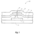
- Figure 1 depicts the formation of a hillock in a metal layer during the fabrication process.
- Figure 2A-2B depict two separate attempts to control the growth of hillocks in metal layers.
- FIG. 3 depicts the multilayered structure made in accordance with the principles of the present invention.
- a hillock is depicted in a thin film structure, such as structure 10. While structure 10 is shown comprising several particular layers, it will be appreciated that the choice of any particular layer is merely made for illustrative purposes and, further, that the problem of hillock formation in metal layers is common to various structures using various materials. Additionally, while structure 10 may resemble a thin film transistor (TFT) in the making, problems of hillock formation are also fatal to metal line crossover formations, capacitors, or any other structure where the breach of a layer's integrity may cause operational malfunction.
- TFT thin film transistor
- Structure 10 comprises substrate 12 (usually glass) upon which a metal layer 14 (e.g. aluminum) is deposited and patterned.
- a bottom dielectric layer 16 (comprising of SiN or the like) acts as an intervening insulator between metal layer 14 and active layer 18.
- a top dielectric layer 20 and another metal line 22 are deposited atop an active layer 18.
- hillock 24 has formed from the metal layer 14 and has "punched” through several layers (layers 16, 18, 20, and 22), creating a "short” between metal layer 14 and metal layer 22.
- a defect such as the one depicted, is most likely fatal to the correct operation of the structure.
- Figure 2A and 2B depict two such attempts.
- Figure 2A shows the capping of a base metal layer 34, such as aluminum, by another metal layer 36, such as tantalum, both deposited upon a substrate 32.
- this method is generally known to be relatively successful in the suppression of hillocks.
- One drawback with this particular method is increased cost of fabrication.
- the additional metal capping layer generally requires a separate masking step. Masking is generally known to be a costly fabrication step.
- FIG. 2A Another drawback of this method is also depicted in Figure 2A - increased line width.
- metal layer 36 is a capping layer, it must extend and register exactly with all sides of the base metal 34.
- the side registration of the capping metal with the base metal adds additional width equal to the sum of distances 37 and 39. Because this additional width is bounded below by the error tolerance of current photolithographic methods, this additional width adds a sizable percentage to the total width.
- the capping metal is usually of higher resistivity than the base metal, the resistivity of the line is greater than a line of the same width comprising only the base metal.
- Figure 2B depicts a second attempt at suppressing the formation of hillocks.
- a metal layer 44 is deposited and patterned on substrate 42. Then, upon the metal layer, an oxide layer 46 is formed upon the metal itself by an anodic process (which is similar to electroplating). This method is employed, for example, on a tantalum metal line, as described in the Shimada et al. article referenced above.
- Figure 3 depicts a multilayered structure 50, made in accordance with the principles of the present invention, for a high performance thin film structure.
- substrate 52 On substrate 52, there is deposited alternating sublayers of base metal 54 and barrier metal 56.
- the base metal is aluminum (Al) and the barrier metal comprises a refractory metal or some alloy thereof such as titanium-tungsten (TiW).
- suitable barrier metals are chromium, molybdenum, tantalum and tungsten, or alloys including at least one of these metals.
- the thin film structure is constructed by a fabrication process that comprises a number of fabrication steps. Each step has an associated temperature. Thus, there is a known maximum temperature for the entire fabrication process to which the Al will be exposed. It is therefore ensured that each deposition of the Al layers is thinner than the critical thickness determined for that maximum temperature.
- the barrier metal is used to prevent adjacent Al layers from merging with each other. It is known that TiW, W and TiN are acceptable barriers for Al up to 550 degrees C.
- the multilayered structure depicted in Figure 3 may have any number of layers greater than two and starting in any particular order desired (e.g. either barrier metal first or base metal first). Additionally, it is unimportant that the all of the barrier metal layers be made of a single metal or alloy. The important aspects of the present invention are that any layer of the base metal is less than the critical thickness and that any two adjacent layers of the base metal is separated by a barrier metal of some type.
- critical thickness for any given fabrication condition is well known to those in the art.
- this critical thickness is known to be about 30 to 80nm, depending upon the particular fabrication conditions.
- a three layer sputter deposited film comprising 60nm of Al, 15nm of TiW and 60nm of Al on a substrate of SiO2 has been shown to withstand 400 degrees C for one hour without hillock formation.
- the sheet resistivity of this film stack is measured to be 0.36 ohm/sq. as opposed to 0.25 ohm/sq. for an Al film (having 2% copper) of the same thickness.
- the present invention is a novel multilayered structure comprising alternating layers of a base metal and a metal selected from a group of barrier metals.
- the base metal in any given layer, is deposited to a thickness less than its critical thickness - a thickness beyond which hillocks are more likely to form for a given temperature.
- a layer of barrier metal is interposed between each such layer of base metal.
- the intervening layer of barrier metal acts to isolate the base metal layers from each other - thus, keeping the effective thickness of each base metal layer below the critical thickness.
- One advantage of the present invention is creating low resistive metal lines for high performance thin film structures. Because the resistivity of a line is inversely proportional to the cross section of the metal layer, the multilayered structure of the present invention offers a greater total cross section of the base metal than a single layer of the base metal - while suppressing the formation of hillocks.
- Another advantage of the present invention is small line widths. Because the barrier metal of the present invention is layered on the base metal, and not capping the base metal, there is no additional width added to the line.
Landscapes
- Physics & Mathematics (AREA)
- Condensed Matter Physics & Semiconductors (AREA)
- General Physics & Mathematics (AREA)
- Engineering & Computer Science (AREA)
- Computer Hardware Design (AREA)
- Microelectronics & Electronic Packaging (AREA)
- Power Engineering (AREA)
- Internal Circuitry In Semiconductor Integrated Circuit Devices (AREA)
- Liquid Crystal (AREA)
Applications Claiming Priority (2)
| Application Number | Priority Date | Filing Date | Title |
|---|---|---|---|
| US08/234,897 US5518805A (en) | 1994-04-28 | 1994-04-28 | Hillock-free multilayer metal lines for high performance thin film structures |
| US234897 | 1994-04-28 |
Publications (3)
| Publication Number | Publication Date |
|---|---|
| EP0681328A2 true EP0681328A2 (fr) | 1995-11-08 |
| EP0681328A3 EP0681328A3 (fr) | 1997-02-12 |
| EP0681328B1 EP0681328B1 (fr) | 2002-01-23 |
Family
ID=22883263
Family Applications (1)
| Application Number | Title | Priority Date | Filing Date |
|---|---|---|---|
| EP19950302791 Expired - Lifetime EP0681328B1 (fr) | 1994-04-28 | 1995-04-26 | Conducteurs métalliques multicouches sans protubérances pour des structures à couches minces à haute performance |
Country Status (4)
| Country | Link |
|---|---|
| US (1) | US5518805A (fr) |
| EP (1) | EP0681328B1 (fr) |
| JP (2) | JPH07302792A (fr) |
| DE (1) | DE69525100T2 (fr) |
Cited By (6)
| Publication number | Priority date | Publication date | Assignee | Title |
|---|---|---|---|---|
| GB2320766A (en) * | 1996-12-30 | 1998-07-01 | Lg Electronics Inc | Liquid crystal displays |
| EP0898785A1 (fr) * | 1996-03-27 | 1999-03-03 | Hyundai Electronics America | Dispositifs d'affichage a matrice active et procede de fabrication |
| EP0979524A1 (fr) * | 1997-04-30 | 2000-02-16 | Candescent Technologies Corporation | Metallisation integree pour dispositifs d'affichage |
| EP1019935A1 (fr) * | 1997-09-30 | 2000-07-19 | Candescent Technologies Corporation | Anodisation d'electrode de rangee |
| US6264813B1 (en) | 1996-12-04 | 2001-07-24 | Aluminum Pechiney | Cathodic sputtering targets made of aluminum alloy |
| DE102004036142A1 (de) * | 2004-07-26 | 2006-03-23 | eupec Europäische Gesellschaft für Leistungshalbleiter mbH | Halbleiterbauelement mit einer Metallisierung sowie Verfahren zu dessen Herstellung |
Families Citing this family (23)
| Publication number | Priority date | Publication date | Assignee | Title |
|---|---|---|---|---|
| JPH0843860A (ja) * | 1994-04-28 | 1996-02-16 | Xerox Corp | 低電圧駆動アクティブ・マトリックス液晶ディスプレイにおける電気的に分離されたピクセル・エレメント |
| US5693983A (en) * | 1994-04-28 | 1997-12-02 | Xerox Corporation | Thin-film structure with conductive molybdenum-chromium line |
| JP3403812B2 (ja) * | 1994-05-31 | 2003-05-06 | 株式会社半導体エネルギー研究所 | 薄膜トランジスタを用いた半導体装置の作製方法 |
| US5608557A (en) * | 1995-01-03 | 1997-03-04 | Xerox Corporation | Circuitry with gate line crossing semiconductor line at two or more channels |
| US5693567A (en) * | 1995-06-07 | 1997-12-02 | Xerox Corporation | Separately etching insulating layer for contacts within array and for peripheral pads |
| US5648674A (en) * | 1995-06-07 | 1997-07-15 | Xerox Corporation | Array circuitry with conductive lines, contact leads, and storage capacitor electrode all formed in layer that includes highly conductive metal |
| JPH10163501A (ja) * | 1996-11-29 | 1998-06-19 | Semiconductor Energy Lab Co Ltd | 絶縁ゲイト型トランジスタ |
| US6222271B1 (en) * | 1997-07-15 | 2001-04-24 | Micron Technology, Inc. | Method of using hydrogen gas in sputter deposition of aluminum-containing films and aluminum-containing films derived therefrom |
| US5969423A (en) * | 1997-07-15 | 1999-10-19 | Micron Technology, Inc. | Aluminum-containing films derived from using hydrogen and oxygen gas in sputter deposition |
| JPH11265938A (ja) * | 1998-03-18 | 1999-09-28 | Toshiba Corp | 半導体装置及びその製造方法 |
| US6057238A (en) * | 1998-03-20 | 2000-05-02 | Micron Technology, Inc. | Method of using hydrogen and oxygen gas in sputter deposition of aluminum-containing films and aluminum-containing films derived therefrom |
| US6396147B1 (en) | 1998-05-16 | 2002-05-28 | Semiconductor Energy Laboratory Co., Ltd. | Semiconductor device with metal-oxide conductors |
| US6380627B1 (en) * | 1998-06-26 | 2002-04-30 | The Regents Of The University Of California | Low resistance barrier layer for isolating, adhering, and passivating copper metal in semiconductor fabrication |
| KR100361570B1 (ko) * | 1999-12-23 | 2002-11-21 | 아남반도체 주식회사 | 반사형 마이크로 액정 표시 장치용 기판 제조 방법 |
| US6780687B2 (en) * | 2000-01-28 | 2004-08-24 | Semiconductor Energy Laboratory Co., Ltd. | Method of manufacturing a semiconductor device having a heat absorbing layer |
| KR100507343B1 (ko) * | 2001-11-28 | 2005-08-08 | 삼성에스디아이 주식회사 | 박막트랜지스터용 금속배선구조 및 그의 형성방법 |
| US7723228B2 (en) * | 2003-05-20 | 2010-05-25 | Applied Materials, Inc. | Reduction of hillocks prior to dielectric barrier deposition in Cu damascene |
| US7371427B2 (en) * | 2003-05-20 | 2008-05-13 | Applied Materials, Inc. | Reduction of hillocks prior to dielectric barrier deposition in Cu damascene |
| JP4729661B2 (ja) * | 2003-07-11 | 2011-07-20 | 奇美電子股▲ふん▼有限公司 | ヒロックが無いアルミニウム層及びその形成方法 |
| DE102004036140A1 (de) * | 2004-07-26 | 2006-03-23 | Infineon Technologies Ag | Halbleiterbauelement |
| US9024327B2 (en) * | 2007-12-14 | 2015-05-05 | Cree, Inc. | Metallization structure for high power microelectronic devices |
| US8822336B2 (en) | 2011-06-16 | 2014-09-02 | United Microelectronics Corp. | Through-silicon via forming method |
| US9018108B2 (en) | 2013-01-25 | 2015-04-28 | Applied Materials, Inc. | Low shrinkage dielectric films |
Citations (4)
| Publication number | Priority date | Publication date | Assignee | Title |
|---|---|---|---|---|
| US4673623A (en) * | 1985-05-06 | 1987-06-16 | The Board Of Trustees Of The Leland Stanford Junior University | Layered and homogeneous films of aluminum and aluminum/silicon with titanium and tungsten for multilevel interconnects |
| EP0253299A1 (fr) * | 1986-07-09 | 1988-01-20 | Siemens Aktiengesellschaft | Métallisation pour circuits intégrés |
| EP0273629A2 (fr) * | 1986-12-29 | 1988-07-06 | Inmos Corporation | Interconnexion en métal de transition pour circuits intégrés |
| EP0304728A2 (fr) * | 1987-08-27 | 1989-03-01 | Siemens Aktiengesellschaft | Procédé de fabrication d'une métallisation plane de faible résistance en aluminium ou en alliage d'aluminium |
Family Cites Families (6)
| Publication number | Priority date | Publication date | Assignee | Title |
|---|---|---|---|---|
| US4522890A (en) * | 1979-10-31 | 1985-06-11 | Illinois Tool Works Inc. | Multilayer high attenuation shielding structure |
| JP2511892B2 (ja) * | 1986-08-08 | 1996-07-03 | 松下電器産業株式会社 | 多層薄膜配線及びその形成方法 |
| DE3783405T2 (de) * | 1986-08-19 | 1993-08-05 | Fujitsu Ltd | Halbleiteranordnung mit einer duennschicht-verdrahtung und verfahren zum herstellen derselben. |
| JPS63155743A (ja) * | 1986-12-19 | 1988-06-28 | Fujitsu Ltd | 半導体装置 |
| US5071714A (en) * | 1989-04-17 | 1991-12-10 | International Business Machines Corporation | Multilayered intermetallic connection for semiconductor devices |
| JPH03222333A (ja) * | 1990-01-26 | 1991-10-01 | Sanyo Electric Co Ltd | 半導体装置の製造方法 |
-
1994
- 1994-04-28 US US08/234,897 patent/US5518805A/en not_active Expired - Lifetime
-
1995
- 1995-04-20 JP JP9523195A patent/JPH07302792A/ja active Pending
- 1995-04-26 EP EP19950302791 patent/EP0681328B1/fr not_active Expired - Lifetime
- 1995-04-26 DE DE1995625100 patent/DE69525100T2/de not_active Expired - Lifetime
-
2008
- 2008-11-12 JP JP2008290125A patent/JP2009044194A/ja active Pending
Patent Citations (4)
| Publication number | Priority date | Publication date | Assignee | Title |
|---|---|---|---|---|
| US4673623A (en) * | 1985-05-06 | 1987-06-16 | The Board Of Trustees Of The Leland Stanford Junior University | Layered and homogeneous films of aluminum and aluminum/silicon with titanium and tungsten for multilevel interconnects |
| EP0253299A1 (fr) * | 1986-07-09 | 1988-01-20 | Siemens Aktiengesellschaft | Métallisation pour circuits intégrés |
| EP0273629A2 (fr) * | 1986-12-29 | 1988-07-06 | Inmos Corporation | Interconnexion en métal de transition pour circuits intégrés |
| EP0304728A2 (fr) * | 1987-08-27 | 1989-03-01 | Siemens Aktiengesellschaft | Procédé de fabrication d'une métallisation plane de faible résistance en aluminium ou en alliage d'aluminium |
Non-Patent Citations (2)
| Title |
|---|
| Journal of Applied Physics, vol. 45, no. 10, 1974, pages 4339-4346 * |
| Journal of Vacuum Science and Technology A, vol. 9, no. 4, 1991, pages 2527-2535 * |
Cited By (11)
| Publication number | Priority date | Publication date | Assignee | Title |
|---|---|---|---|---|
| EP0898785A1 (fr) * | 1996-03-27 | 1999-03-03 | Hyundai Electronics America | Dispositifs d'affichage a matrice active et procede de fabrication |
| EP0898785A4 (fr) * | 1996-03-27 | 2002-03-13 | Hyundai Electronics America | Dispositifs d'affichage a matrice active et procede de fabrication |
| US6264813B1 (en) | 1996-12-04 | 2001-07-24 | Aluminum Pechiney | Cathodic sputtering targets made of aluminum alloy |
| GB2320766A (en) * | 1996-12-30 | 1998-07-01 | Lg Electronics Inc | Liquid crystal displays |
| GB2320766B (en) * | 1996-12-30 | 1999-08-11 | Lg Electronics Inc | Liquid crystal displays |
| EP0979524A1 (fr) * | 1997-04-30 | 2000-02-16 | Candescent Technologies Corporation | Metallisation integree pour dispositifs d'affichage |
| EP0979524A4 (fr) * | 1997-04-30 | 2002-10-16 | Candescent Intellectual Prop | Metallisation integree pour dispositifs d'affichage |
| EP1019935A1 (fr) * | 1997-09-30 | 2000-07-19 | Candescent Technologies Corporation | Anodisation d'electrode de rangee |
| EP1019935A4 (fr) * | 1997-09-30 | 2004-04-07 | Candescent Tech Corp | Anodisation d'electrode de rangee |
| DE102004036142A1 (de) * | 2004-07-26 | 2006-03-23 | eupec Europäische Gesellschaft für Leistungshalbleiter mbH | Halbleiterbauelement mit einer Metallisierung sowie Verfahren zu dessen Herstellung |
| DE102004036142B4 (de) * | 2004-07-26 | 2009-04-09 | Infineon Technologies Ag | Halbleiterbauelement mit einer Metallisierung mit mehreren durch zumindest eine Barriereschicht getrennten Metallisierungsschichten sowie Verfahren zu dessen Herstellung |
Also Published As
| Publication number | Publication date |
|---|---|
| DE69525100D1 (de) | 2002-03-14 |
| JP2009044194A (ja) | 2009-02-26 |
| JPH07302792A (ja) | 1995-11-14 |
| EP0681328B1 (fr) | 2002-01-23 |
| DE69525100T2 (de) | 2002-07-18 |
| US5518805A (en) | 1996-05-21 |
| EP0681328A3 (fr) | 1997-02-12 |
Similar Documents
| Publication | Publication Date | Title |
|---|---|---|
| US5518805A (en) | Hillock-free multilayer metal lines for high performance thin film structures | |
| US4905066A (en) | Thin-film transistor | |
| JP3226223B2 (ja) | 薄膜トランジスタアレイ装置および液晶表示装置 | |
| CN101552225B (zh) | 制备接触部分及薄膜晶体管阵列面板的方法 | |
| US7981761B2 (en) | Method of manufacturing semiconductor device having MIM capacitor | |
| EP0973020B1 (fr) | Capteur de température électrique comprenant une multi-couche | |
| EP0483958A1 (fr) | Anti-fusible à programmation électrique comprenant une couche intermédiaire diélectrique et une couche intermédiaire en silicium amorphe | |
| KR0186206B1 (ko) | 액정표시소자 및 그의 제조방법 | |
| KR970004885B1 (ko) | 평판표시장치 및 그 제조방법 | |
| KR20070003719A (ko) | 박막 트랜지스터 회로 장치의 제조 방법 | |
| JPH06188419A (ja) | 薄膜トランジスタの製造方法 | |
| EP0680079A2 (fr) | Structure topographique en couches minces à profil conique | |
| GB2134707A (en) | Thin film transistor with laminated source and drain electrodes and method of manufacture | |
| EP0922301B1 (fr) | Substrat a conducteur en alliage d'aluminium faible resistance | |
| JPH02211426A (ja) | 液晶表示装置およびその製造方法 | |
| US5738948A (en) | Electrode-wiring material and electrode-wiring substrate using the same | |
| KR100208024B1 (ko) | 힐락 억제를 위한 tft의 알루미늄 게이트 구조 및 그 제조방법 | |
| JP3707704B2 (ja) | 配線材料、液晶ディスプレー装置、および配線層の形成方法 | |
| EP0681327A2 (fr) | Double couche diélectrique de couverture pour supprimer des protubérances dans les couches métalliques des structures à couches minces | |
| JP2740591B2 (ja) | 半導体装置の製造方法 | |
| EP0680088A1 (fr) | Structure à mince couche avec une ligne conductrice au molybdene-chrome | |
| JP3245613B2 (ja) | 薄膜素子の製造方法 | |
| EP0731507A1 (fr) | Matériaux d'électrodes | |
| US20020014701A1 (en) | Interconnect structure for semiconductor device and method of fabrication | |
| JP3087704B2 (ja) | 半導体装置及びその製造方法 |
Legal Events
| Date | Code | Title | Description |
|---|---|---|---|
| PUAI | Public reference made under article 153(3) epc to a published international application that has entered the european phase |
Free format text: ORIGINAL CODE: 0009012 |
|
| AK | Designated contracting states |
Kind code of ref document: A2 Designated state(s): DE FR GB |
|
| PUAL | Search report despatched |
Free format text: ORIGINAL CODE: 0009013 |
|
| AK | Designated contracting states |
Kind code of ref document: A3 Designated state(s): DE FR GB |
|
| 17P | Request for examination filed |
Effective date: 19970812 |
|
| 17Q | First examination report despatched |
Effective date: 19980519 |
|
| GRAG | Despatch of communication of intention to grant |
Free format text: ORIGINAL CODE: EPIDOS AGRA |
|
| GRAG | Despatch of communication of intention to grant |
Free format text: ORIGINAL CODE: EPIDOS AGRA |
|
| GRAH | Despatch of communication of intention to grant a patent |
Free format text: ORIGINAL CODE: EPIDOS IGRA |
|
| GRAH | Despatch of communication of intention to grant a patent |
Free format text: ORIGINAL CODE: EPIDOS IGRA |
|
| GRAA | (expected) grant |
Free format text: ORIGINAL CODE: 0009210 |
|
| REG | Reference to a national code |
Ref country code: GB Ref legal event code: IF02 |
|
| AK | Designated contracting states |
Kind code of ref document: B1 Designated state(s): DE FR GB |
|
| REF | Corresponds to: |
Ref document number: 69525100 Country of ref document: DE Date of ref document: 20020314 |
|
| ET | Fr: translation filed | ||
| PLBE | No opposition filed within time limit |
Free format text: ORIGINAL CODE: 0009261 |
|
| STAA | Information on the status of an ep patent application or granted ep patent |
Free format text: STATUS: NO OPPOSITION FILED WITHIN TIME LIMIT |
|
| 26N | No opposition filed | ||
| PGFP | Annual fee paid to national office [announced via postgrant information from national office to epo] |
Ref country code: GB Payment date: 20140428 Year of fee payment: 20 |
|
| PGFP | Annual fee paid to national office [announced via postgrant information from national office to epo] |
Ref country code: DE Payment date: 20140425 Year of fee payment: 20 Ref country code: FR Payment date: 20140418 Year of fee payment: 20 |
|
| REG | Reference to a national code |
Ref country code: DE Ref legal event code: R071 Ref document number: 69525100 Country of ref document: DE |
|
| REG | Reference to a national code |
Ref country code: GB Ref legal event code: PE20 Expiry date: 20150425 |
|
| PG25 | Lapsed in a contracting state [announced via postgrant information from national office to epo] |
Ref country code: GB Free format text: LAPSE BECAUSE OF EXPIRATION OF PROTECTION Effective date: 20150425 |