EP0664051B1 - METHOD FOR FORMING THIN TUNNELING WINDOWS IN EEPROMs - Google Patents
METHOD FOR FORMING THIN TUNNELING WINDOWS IN EEPROMs Download PDFInfo
- Publication number
- EP0664051B1 EP0664051B1 EP94922441A EP94922441A EP0664051B1 EP 0664051 B1 EP0664051 B1 EP 0664051B1 EP 94922441 A EP94922441 A EP 94922441A EP 94922441 A EP94922441 A EP 94922441A EP 0664051 B1 EP0664051 B1 EP 0664051B1
- Authority
- EP
- European Patent Office
- Prior art keywords
- oxide
- oxide layer
- layer
- substrate
- mask
- Prior art date
- Legal status (The legal status is an assumption and is not a legal conclusion. Google has not performed a legal analysis and makes no representation as to the accuracy of the status listed.)
- Expired - Lifetime
Links
- 238000000034 method Methods 0.000 title claims description 22
- 230000005641 tunneling Effects 0.000 title claims description 13
- 150000004767 nitrides Chemical class 0.000 claims description 41
- 239000000758 substrate Substances 0.000 claims description 41
- 238000007667 floating Methods 0.000 claims description 23
- 238000005530 etching Methods 0.000 claims description 13
- XUIMIQQOPSSXEZ-UHFFFAOYSA-N Silicon Chemical compound [Si] XUIMIQQOPSSXEZ-UHFFFAOYSA-N 0.000 claims description 7
- 238000000151 deposition Methods 0.000 claims description 7
- 229910021420 polycrystalline silicon Inorganic materials 0.000 claims description 7
- 229910052710 silicon Inorganic materials 0.000 claims description 7
- 239000010703 silicon Substances 0.000 claims description 7
- 238000000206 photolithography Methods 0.000 claims description 6
- 238000000059 patterning Methods 0.000 claims description 3
- 239000010410 layer Substances 0.000 description 71
- KRHYYFGTRYWZRS-UHFFFAOYSA-N Fluorane Chemical compound F KRHYYFGTRYWZRS-UHFFFAOYSA-N 0.000 description 6
- 229920002120 photoresistant polymer Polymers 0.000 description 6
- 230000008569 process Effects 0.000 description 6
- 229910052581 Si3N4 Inorganic materials 0.000 description 4
- VYPSYNLAJGMNEJ-UHFFFAOYSA-N Silicium dioxide Chemical compound O=[Si]=O VYPSYNLAJGMNEJ-UHFFFAOYSA-N 0.000 description 4
- 238000007796 conventional method Methods 0.000 description 3
- 230000008878 coupling Effects 0.000 description 3
- 238000010168 coupling process Methods 0.000 description 3
- 238000005859 coupling reaction Methods 0.000 description 3
- 239000004065 semiconductor Substances 0.000 description 3
- HQVNEWCFYHHQES-UHFFFAOYSA-N silicon nitride Chemical compound N12[Si]34N5[Si]62N3[Si]51N64 HQVNEWCFYHHQES-UHFFFAOYSA-N 0.000 description 3
- 230000008021 deposition Effects 0.000 description 2
- 239000002019 doping agent Substances 0.000 description 2
- 238000005468 ion implantation Methods 0.000 description 2
- 150000002500 ions Chemical class 0.000 description 2
- 238000001459 lithography Methods 0.000 description 2
- 238000004518 low pressure chemical vapour deposition Methods 0.000 description 2
- 238000004519 manufacturing process Methods 0.000 description 2
- 239000000377 silicon dioxide Substances 0.000 description 2
- 241000293849 Cordylanthus Species 0.000 description 1
- -1 Si3N4 Chemical compound 0.000 description 1
- 238000001015 X-ray lithography Methods 0.000 description 1
- 238000013459 approach Methods 0.000 description 1
- 238000003491 array Methods 0.000 description 1
- 230000015572 biosynthetic process Effects 0.000 description 1
- 229910052681 coesite Inorganic materials 0.000 description 1
- 229910052906 cristobalite Inorganic materials 0.000 description 1
- 238000007599 discharging Methods 0.000 description 1
- 230000000694 effects Effects 0.000 description 1
- 238000005265 energy consumption Methods 0.000 description 1
- 238000005516 engineering process Methods 0.000 description 1
- 238000010849 ion bombardment Methods 0.000 description 1
- 229910044991 metal oxide Inorganic materials 0.000 description 1
- 150000004706 metal oxides Chemical class 0.000 description 1
- 230000003287 optical effect Effects 0.000 description 1
- 238000012856 packing Methods 0.000 description 1
- 230000009467 reduction Effects 0.000 description 1
- 235000012239 silicon dioxide Nutrition 0.000 description 1
- 239000002356 single layer Substances 0.000 description 1
- 229910052682 stishovite Inorganic materials 0.000 description 1
- 238000003860 storage Methods 0.000 description 1
- 239000000126 substance Substances 0.000 description 1
- 239000002344 surface layer Substances 0.000 description 1
- 229910052905 tridymite Inorganic materials 0.000 description 1
Images


Classifications
-
- H—ELECTRICITY
- H10—SEMICONDUCTOR DEVICES; ELECTRIC SOLID-STATE DEVICES NOT OTHERWISE PROVIDED FOR
- H10B—ELECTRONIC MEMORY DEVICES
- H10B41/00—Electrically erasable-and-programmable ROM [EEPROM] devices comprising floating gates
- H10B41/30—Electrically erasable-and-programmable ROM [EEPROM] devices comprising floating gates characterised by the memory core region
- H10B41/35—Electrically erasable-and-programmable ROM [EEPROM] devices comprising floating gates characterised by the memory core region with a cell select transistor, e.g. NAND
-
- H—ELECTRICITY
- H01—ELECTRIC ELEMENTS
- H01L—SEMICONDUCTOR DEVICES NOT COVERED BY CLASS H10
- H01L21/00—Processes or apparatus adapted for the manufacture or treatment of semiconductor or solid state devices or of parts thereof
- H01L21/02—Manufacture or treatment of semiconductor devices or of parts thereof
- H01L21/02104—Forming layers
- H01L21/02365—Forming inorganic semiconducting materials on a substrate
- H01L21/02518—Deposited layers
- H01L21/02521—Materials
- H01L21/02538—Group 13/15 materials
- H01L21/0254—Nitrides
-
- H—ELECTRICITY
- H01—ELECTRIC ELEMENTS
- H01L—SEMICONDUCTOR DEVICES NOT COVERED BY CLASS H10
- H01L21/00—Processes or apparatus adapted for the manufacture or treatment of semiconductor or solid state devices or of parts thereof
- H01L21/02—Manufacture or treatment of semiconductor devices or of parts thereof
- H01L21/02104—Forming layers
- H01L21/02365—Forming inorganic semiconducting materials on a substrate
- H01L21/02518—Deposited layers
- H01L21/02521—Materials
- H01L21/02551—Group 12/16 materials
- H01L21/02554—Oxides
-
- H—ELECTRICITY
- H01—ELECTRIC ELEMENTS
- H01L—SEMICONDUCTOR DEVICES NOT COVERED BY CLASS H10
- H01L21/00—Processes or apparatus adapted for the manufacture or treatment of semiconductor or solid state devices or of parts thereof
- H01L21/02—Manufacture or treatment of semiconductor devices or of parts thereof
- H01L21/027—Making masks on semiconductor bodies for further photolithographic processing not provided for in group H01L21/18 or H01L21/34
- H01L21/0271—Making masks on semiconductor bodies for further photolithographic processing not provided for in group H01L21/18 or H01L21/34 comprising organic layers
- H01L21/0273—Making masks on semiconductor bodies for further photolithographic processing not provided for in group H01L21/18 or H01L21/34 comprising organic layers characterised by the treatment of photoresist layers
- H01L21/0274—Photolithographic processes
-
- H—ELECTRICITY
- H10—SEMICONDUCTOR DEVICES; ELECTRIC SOLID-STATE DEVICES NOT OTHERWISE PROVIDED FOR
- H10D—INORGANIC ELECTRIC SEMICONDUCTOR DEVICES
- H10D30/00—Field-effect transistors [FET]
- H10D30/60—Insulated-gate field-effect transistors [IGFET]
- H10D30/68—Floating-gate IGFETs
- H10D30/681—Floating-gate IGFETs having only two programming levels
- H10D30/684—Floating-gate IGFETs having only two programming levels programmed by hot carrier injection
-
- Y—GENERAL TAGGING OF NEW TECHNOLOGICAL DEVELOPMENTS; GENERAL TAGGING OF CROSS-SECTIONAL TECHNOLOGIES SPANNING OVER SEVERAL SECTIONS OF THE IPC; TECHNICAL SUBJECTS COVERED BY FORMER USPC CROSS-REFERENCE ART COLLECTIONS [XRACs] AND DIGESTS
- Y10—TECHNICAL SUBJECTS COVERED BY FORMER USPC
- Y10S—TECHNICAL SUBJECTS COVERED BY FORMER USPC CROSS-REFERENCE ART COLLECTIONS [XRACs] AND DIGESTS
- Y10S148/00—Metal treatment
- Y10S148/117—Oxidation, selective
-
- Y—GENERAL TAGGING OF NEW TECHNOLOGICAL DEVELOPMENTS; GENERAL TAGGING OF CROSS-SECTIONAL TECHNOLOGIES SPANNING OVER SEVERAL SECTIONS OF THE IPC; TECHNICAL SUBJECTS COVERED BY FORMER USPC CROSS-REFERENCE ART COLLECTIONS [XRACs] AND DIGESTS
- Y10—TECHNICAL SUBJECTS COVERED BY FORMER USPC
- Y10S—TECHNICAL SUBJECTS COVERED BY FORMER USPC CROSS-REFERENCE ART COLLECTIONS [XRACs] AND DIGESTS
- Y10S148/00—Metal treatment
- Y10S148/163—Thick-thin oxides
-
- Y—GENERAL TAGGING OF NEW TECHNOLOGICAL DEVELOPMENTS; GENERAL TAGGING OF CROSS-SECTIONAL TECHNOLOGIES SPANNING OVER SEVERAL SECTIONS OF THE IPC; TECHNICAL SUBJECTS COVERED BY FORMER USPC CROSS-REFERENCE ART COLLECTIONS [XRACs] AND DIGESTS
- Y10—TECHNICAL SUBJECTS COVERED BY FORMER USPC
- Y10S—TECHNICAL SUBJECTS COVERED BY FORMER USPC CROSS-REFERENCE ART COLLECTIONS [XRACs] AND DIGESTS
- Y10S438/00—Semiconductor device manufacturing: process
- Y10S438/981—Utilizing varying dielectric thickness
Definitions
- the present invention relates generally to methods of fabricating a semiconductor non-volatile memory device and more particularly to fabricating thin dielectric windows for electron tunneling in electrically erasable programmable read only memory devices.
- MOS metal oxide semiconductor
- EEPROM electrically erasable, programmable read only memory
- the area of the thin dielectric layer through which electron tunneling occurs is limited to small generally rectangular dimensions and the thinness of the layer is carefully controlled. For this reason the rectangular area is termed a "window.”
- Oxide windows having a thickness of between 7 nm (70 angstroms) to 20 nm (200 angstroms) and an area of one half to several square microns are typical.
- U.S. Pat. No. 4,590,503 to Harari describes formation of a thin tunnel oxide region.
- a silicon substrate that has been doped with ions is located below the floating gate, separated by a dielectric layer.
- the thin tunnel oxide window dielectric separating the floating gate layer from the substrate provides the region for electrons to tunnel between the substrate and the floating gate.
- the area and the thickness of the tunnel oxide window are two of the most important factors in the performance of EEPROM memory cells. For any significant tunneling to occur, the difference in voltage between the floating gate and the substrate must exceed a threshold voltage, the threshold voltage being generally related to the both the area and thickness of the tunneling window.
- the sense gate affects the floating gate through capacitive coupling, and a similar capacitive coupling exists between the floating gate and the substrate. Since the voltage difference between the sense gate and the substrate is the sum of the voltage difference between the floating gate and the substrate and the voltage difference between the floating gate and the sense gate, a lower threshold voltage allows a lower voltage to be applied between the sense gate and the substrate for charging and discharging. Alternatively, a lower threshold voltage allows the memory cell to be charged or discharged more quickly, entailing a higher tunneling current.
- a smaller tunneling window area is advantageous in at least three ways.
- a smaller window allows the memory cell to be read or written either with a lower applied voltage or more quickly, or both.
- Each of these possibilities offers user benefits, such as an increase in programming speed or a reduction in energy consumption.
- a smaller window area allows the cell and the whole transistor circuit to be made smaller, and the resultant scaling down in size of large arrays of such circuits has the benefits of packing more information capabilities in a smaller package.
- a smaller tunneling window offers the promise of better performance and more memory in a smaller package.
- a smaller window area allows the possibility of lowering write and erase voltages.
- the tunnel oxide window is typically produced during the fabrication of the EEPROM by the deposition of layers and etching by conventional photoresist techniques. As the area of tunnel oxide windows approaches and even becomes smaller than the resolution of the photoresist patterning and etching, conventional photoresist techniques present a limit to the size that these windows can be accurately made.
- JP-A-2 021 664 an EEPROM device is disclosed having a dielectric tunnel window.
- the device is formed by patterning a silicon nitride mask.
- the device of the Japanese disclosure does not solve the object of the invention as stated above.
- a submicron area tunnel window is made in an EEPROM by forming a pattern for the window to dimensions smaller than that permitted by the limits of lithography.
- the window is formed by undercutting a precise amount of an end of a nitride layer that has been etched by conventional photoresist techniques, and subsequently depositing and etching layers to form that small undercut area into a dielectric window.
- a thin oxide layer approximately 50 nm (500 angstroms) in thickness, on top of a silicon substrate which has been or can be implanted with ions in spots to form regions of enhanced charge for forming source and drain electrodes, and which also has been grown with field oxide boundaries separating enhanced charge regions.
- the field oxide forms borders between memory cells.
- a thin silicon nitride, i.e. Si 3 N 4 , "nitride", layer approximately 100 nm (1000 angstroms) in thickness is deposited on the oxide layer.
- the nitride layer is then masked and etched so that, for each pair of memory cells to be formed, only a plateau shaped nitride layer remains, two opposite ends of the plateau located approximately above the eventual location of two tunnel oxide windows.
- a self aligned, to the tunnel, buried N+ region is desired, it may be added at this point by ion implantation bombardment near the ends of the nitride plateau.
- the oxide layer is then wet etched with buffered hydrofluoric acid or any other oxide etch that does not damage the silicon substrate, removing not only the oxide that is not covered by the plateau, but also etching slightly under the ends of the plateau a precise amount which may be a hundred to several hundred nm (thousand to several thousand angstroms), exposing the substrate where the oxide has been etched away. The amount of this undercut will determine the size of the tunnel oxide window.
- an oxide layer much thinner than the original oxide layer is grown on the substrate, including the area of the substrate lying under the ends of the nitride plateau.
- a layer of nitride, approximately 40 nm (400 angstroms) thick, is then deposited using low pressure chemical vapor deposition techniques, causing the space beneath the nitride ends and above the oxide layer to be filled in with nitride. Then a blanket nitride etch that removes about 50 nm (500 angstroms) is applied.
- nitride filling in the space beneath the nitride ends and above the oxide layer, as it is protected from etching by the approximately 40 nm (400 Angstrom) layer of nitride.
- a layer of oxide is then grown on the approximately 10 nm (100 angstrom) thick layer of oxide not covered by the nitride, forming a single layer of oxide approximately 70 nm (700 angstroms) in thickness.
- the nitride is then stripped off, leaving only the substrate blanketed by three layers of oxide: the approximately 50 nm (500 angstrom) thick layer that was not covered by nitride, the approximately 50 nm (500 angstrom) thick layer that has been under the nitride plateau and has never been etched, and between those layers the approximately 10 nm (100 angstrom) thick layer that was under the ends of the nitride plateau.
- a buffered wet oxide etch is applied that removes approximately 12 nm (120 angstroms) of oxide, including all of the approximately 10 nm (100 angstrom) thick layer that was under the ends of the nitride plateau.
- An approximately 8 nm (80 angstrom) thick layer of oxide is then grown. This thin layer, where it is grown on the small area of exposed substrate that formerly was under the ends of the nitride plateau, is to become the tunneling window.
- a conventional EEPROM fabrication process is then followed, beginning with the deposit of a polycrystalline silicon layer that is to become the floating gate.
- a bottom surface of a gate made of this layer can be seen to be separated from the substrate by several hundred angstroms of oxide, except for the small tunneling window area, which is separated from the substrate by only approximately 8 nm (80 angstroms) of oxide.
- the field oxide rows provide borders to the tunnel oxide window that may be a hundred to thousand nm (thousand to ten thousand angstroms) apart.
- the nitride undercut technique described above has produced a window in a direction perpendicular to that which is of a size one hundred to several hundred nm (one thousand to several thousand angstroms).
- the tunnel window produced by the present invention may be much less than one square micron in area, by less than 10 nm (one hundred angstroms) in thickness.
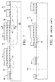
- Fig. 1 is a cross-sectional elevation view of a portion of a semiconductor substrate having doped regions under layers of oxide and nitride above the substrate.
- Fig. 2 is a cross-sectional elevation view of the elements of Fig. 1 after the layers have been masked and etched.
- Fig. 3 is a cross-sectional elevation view of the elements of Fig. 2 after a layer of oxide has been grown and a layer of nitride has been deposited.
- Fig. 4 is a cross-sectional elevation view of the elements of Fig. 3 after a layer of the nitride has been etched away.
- Fig. 5 is a cross-sectional elevation view of the elements of Fig. 4 after a layer of oxide has been grown.
- Fig. 6 is a cross-sectional elevation view of the elements of Fig. 5 after the nitride has been stripped away, a layer of oxide has been etched and another layer of oxide has been grown.
- Fig. 7 is a cross-sectional elevation view of an EEPROM device constructed in accordance with this invention.
- Fig. 8 is a cross-sectional elevation view of a conventional EEPROM device.
- Fig. 9 is a perpendicular cross-sectional elevation view of an EEPROM device constructed in accordance with this invention.
- a silicon substrate 15 having three buried N+ regions 20 is shown.
- the N+ regions 20 are formed by conventional methods, such as ion implantation of an N type dopant.
- Subsurface doped regions are typically used as source and drain electrodes of an MOS transistor.
- a first oxide layer 25 which is approximately 50 nm (500 angstroms) in thickness.
- a first nitride layer 30 which is approximately 100 nm (1000 angstroms in thickness).
- Fig. 2 shows the substrate 15, and the oxide layer 25 and nitride layer 30 after etching.
- the nitride layer 30 has been masked and etched by conventional methods to leave a plateau 32 located above one of the buried N+ regions 20 having ends 35 located above the other two buried N+ regions 20. If a self-aligned (to the tunnel) buried N+ region is desired, it may be formed at this point in this embodiment. For this case there would be no buried N+ regions 20 present in Fig. 1.
- an N type dopant is implanted by ion bombardment. This will form the left and right buried regions 20 shown in Fig. 2.
- a wet oxide etch of hydrofluoric acid or any other chemical known to etch oxide without damaging the silicon substrate has been applied that not only removes all of the oxide layer 25 that not covered by the plateau 32, but also etches undercuts 40 in the oxide layer 25 slightly under the ends 35 of the plateau 32.
- the amount of these slight undercuts 40 can be accurately controlled by known etching techniques and may be a hundred to several hundred nm (thousand to several thousand angstroms) under the ends 35.
- a thin second layer 45 of oxide is grown next.
- This oxide layer 45 may be about 10 nm (100 angstroms) in thickness and is formed along the exposed silicon substrate 15 including the undercuts 40, leaving spaces 47 between the ends 35 and the undercuts 40.
- the oxide layer 45 does not grow on the nitride plateau 32.
- a blanket second layer 50 of nitride is then deposited that covers the plateau 32, the oxide layer 45 and the undercuts 40, and fills the spaces 47.
- the nitride layer 50 may be deposited by low pressure chemical vapor deposition and may be approximately 400 angstroms in thickness.
- a blanket nitride etch is next applied that removes approximately 500 angstroms of nitride, removing substantially all of the nitride layer 50 except that which filled in the spaces 47, which is protected by other parts of layer 50 which are exposed to the etch first.
- a third layer 55 of oxide is grown on all of the oxide that is not covered by nitride.
- This oxide layer 55 combines with the second layer 45 of oxide that is not located below a nitride layer and also diffuses into a thin surface layer of the substrate below.
- the third layer 55 of oxide may be about 70 nm (700 angstroms) in thickness.
- a top oxide etch is then applied to remove any oxide grown on the nitride features 32 and 47.
- a nitride strip is applied that removes all of the remaining nitride.
- small lengths of the thin second oxide layer 45 from the undercuts 40 are left between the first oxide layer 25 and the third oxide layer 55, both of which are approximately 50 nm (500 angstroms) thick.
- a buffered oxide etch which may utilize hydrofluoric acid is applied to remove approximately 12 nm (120 angstroms) of oxide. This removes all of the second oxide layer 45 from the undercut, exposing but not damaging a small area of the substrate 15 between the layers 25 and 55 of oxide.
- a thin fourth layer 60 of oxide is then grown or deposited on the small exposed area of the substrate 15 and the layers 25 and 55. This layer 60 of oxide may be approximately 8 nm (80 angstroms) in thickness, and becomes a tunnel oxide window 65 where it covers the small area of substrate 15 that had previously been etched of all oxide.
- a standard EEPROM process flow would be followed, beginning with the deposition of a first polycrystalline silicon layer to form a floating gate.
- FIG. 7 an EEPROM cell having tunnel oxide windows 65 formed with the process of the present invention is shown.
- This EEPROM cell can be seen to have polycrystalline silicon floating gates 70, and sense gates 75 and control gates 80 formed from another polycrystalline silicon deposit.
- a pair of cells is symmetrical about mirror line 85, and the distance 88 between those lines represents the length of one cell.
- a prior art EEPROM cell is shown in Fig. 8.
- the prior art cell a pair of which is symmetrical about mirror lines 90 and 92, has tunnel oxide windows 95 that are substantially larger than the tunnel oxide windows 65 of the present invention.
- the prior art cell also has a floating gate 98, sense gate 100 and control gate 105 that are larger than the floating gate 70, sense gate 75 and control gates 80 of the present invention.
- the present invention allows not only smaller EEPROM tunnel oxide windows than the prior art, with the improvements in performance previously described, but also allows the whole EEPROM cell to be scaled to a smaller size which allows more EEPROM cells to be packed together.
- field oxide regions 110 separating each cell 112 were grown by conventional techniques onto and into the substrate 15 before the growth or deposit of first oxide layer 25.
- the distance 115 between those field oxide regions 110 determines one dimension of the tunnel window 65, and may be a hundred to thousand nm (thousand to ten thousand angstroms).
- the floating gates 70 can be seen to contour upward away from the tunnel window 65 to fit on top of the field oxide regions 110, and the sense gates 75 are similarly contoured.
- the sense gates 75 wrap around ends of the floating gates 70, in order to increase the capacitive coupling between these gates.
- the tunnel oxide windows 65 may be less than 10 nm (one hundred angstroms) in thickness, and may be as small as one hundred nm (thousand angstroms) in each dimension of area, a substantial decrease in size compared to the prior art.
- the dimensions of the thin oxide tunneling window have been characterized as being smaller than dimensions resolvable by photolithography.
- the photolithography which is referred to is carried out at optical wavelengths using diffraction limited optics.
- No reference is intended to x-ray lithography which can resolve distances much smaller than the distance resolved by conventional photolithography. Such reference or comparison is not intended because the thin oxide windows of the present invention have not been measured relative to such distances.
Landscapes
- Engineering & Computer Science (AREA)
- Physics & Mathematics (AREA)
- Condensed Matter Physics & Semiconductors (AREA)
- General Physics & Mathematics (AREA)
- Manufacturing & Machinery (AREA)
- Computer Hardware Design (AREA)
- Microelectronics & Electronic Packaging (AREA)
- Power Engineering (AREA)
- Non-Volatile Memory (AREA)
- Semiconductor Memories (AREA)
Applications Claiming Priority (3)
| Application Number | Priority Date | Filing Date | Title |
|---|---|---|---|
| US08/100,467 US5352618A (en) | 1993-07-30 | 1993-07-30 | Method for forming thin tunneling windows in EEPROMs |
| US100467 | 1993-07-30 | ||
| PCT/US1994/006860 WO1995004371A1 (en) | 1993-07-30 | 1994-06-17 | METHOD FOR FORMING THIN TUNNELING WINDOWS IN EEPROMs |
Publications (3)
| Publication Number | Publication Date |
|---|---|
| EP0664051A1 EP0664051A1 (en) | 1995-07-26 |
| EP0664051A4 EP0664051A4 (en) | 1996-01-10 |
| EP0664051B1 true EP0664051B1 (en) | 1999-05-12 |
Family
ID=22279908
Family Applications (1)
| Application Number | Title | Priority Date | Filing Date |
|---|---|---|---|
| EP94922441A Expired - Lifetime EP0664051B1 (en) | 1993-07-30 | 1994-06-17 | METHOD FOR FORMING THIN TUNNELING WINDOWS IN EEPROMs |
Country Status (8)
| Country | Link |
|---|---|
| US (1) | US5352618A (enExample) |
| EP (1) | EP0664051B1 (enExample) |
| JP (1) | JP3729849B2 (enExample) |
| KR (1) | KR100297301B1 (enExample) |
| CN (1) | CN1045348C (enExample) |
| DE (1) | DE69418447T2 (enExample) |
| TW (1) | TW248615B (enExample) |
| WO (1) | WO1995004371A1 (enExample) |
Families Citing this family (15)
| Publication number | Priority date | Publication date | Assignee | Title |
|---|---|---|---|---|
| US5429960A (en) * | 1994-11-28 | 1995-07-04 | United Microelectronics Corporation | Method of making flash EEPROM memory |
| US5521109A (en) * | 1995-09-01 | 1996-05-28 | United Microelectronics Corp. | Method for fabricating a high coupling ratio flash memory with a very narrow tunnel layer |
| US5963806A (en) * | 1996-12-09 | 1999-10-05 | Mosel Vitelic, Inc. | Method of forming memory cell with built-in erasure feature |
| US5895240A (en) * | 1997-06-30 | 1999-04-20 | Taiwan Semiconductor Manufacturing Company, Ltd. | Method of making stepped edge structure of an EEPROM tunneling window |
| US5918133A (en) * | 1997-12-18 | 1999-06-29 | Advanced Micro Devices | Semiconductor device having dual gate dielectric thickness along the channel and fabrication thereof |
| US6255165B1 (en) * | 1999-10-18 | 2001-07-03 | Advanced Micro Devices, Inc. | Nitride plug to reduce gate edge lifting |
| US6518072B1 (en) * | 1999-11-05 | 2003-02-11 | Advanced Micro Devices, Inc. | Deposited screen oxide for reducing gate edge lifting |
| US20060073509A1 (en) * | 1999-11-18 | 2006-04-06 | Michael Kilpatrick | Method for detecting and quantitating multiple subcellular components |
| US6624027B1 (en) | 2002-05-09 | 2003-09-23 | Atmel Corporation | Ultra small thin windows in floating gate transistors defined by lost nitride spacers |
| US6905926B2 (en) * | 2003-09-04 | 2005-06-14 | Atmel Corporation | Method of making nonvolatile transistor pairs with shared control gate |
| US7161203B2 (en) * | 2004-06-04 | 2007-01-09 | Micron Technology, Inc. | Gated field effect device comprising gate dielectric having different K regions |
| US7553704B2 (en) * | 2005-06-28 | 2009-06-30 | Freescale Semiconductor, Inc. | Antifuse element and method of manufacture |
| US7528015B2 (en) * | 2005-06-28 | 2009-05-05 | Freescale Semiconductor, Inc. | Tunable antifuse element and method of manufacture |
| CN106816368B (zh) * | 2015-12-01 | 2019-11-05 | 中芯国际集成电路制造(上海)有限公司 | 半导体结构和cmos晶体管的形成方法 |
| CN114551452A (zh) * | 2016-10-21 | 2022-05-27 | 联华电子股份有限公司 | 单层多晶硅电子抹除式可复写只读存储器 |
Family Cites Families (7)
| Publication number | Priority date | Publication date | Assignee | Title |
|---|---|---|---|---|
| US4817561A (en) * | 1986-12-17 | 1989-04-04 | Ichthyotech, Ltd. | Aquatic aeration and filtering system |
| US4755477A (en) * | 1987-03-24 | 1988-07-05 | Industrial Technology Research Institute | Overhang isolation technology |
| JP2701332B2 (ja) | 1988-07-08 | 1998-01-21 | 日本電気株式会社 | 浮遊ゲート型不揮発性半導体記憶装置の製造方法 |
| US4941822A (en) * | 1989-07-20 | 1990-07-17 | Marvin Evans | Apparatus for heat treating contaminated particulate material |
| CN2078413U (zh) * | 1990-10-13 | 1991-06-05 | 福建省宁德市茶叶机械制造厂 | 连续反烧燃煤装置 |
| US5216270A (en) * | 1991-02-28 | 1993-06-01 | Texas Instruments Incorporated | Non-volatile memory cell with tunnel window structure and method |
| US5236862A (en) * | 1992-12-03 | 1993-08-17 | Motorola, Inc. | Method of forming oxide isolation |
-
1993
- 1993-07-30 US US08/100,467 patent/US5352618A/en not_active Expired - Lifetime
-
1994
- 1994-06-17 JP JP50581295A patent/JP3729849B2/ja not_active Expired - Fee Related
- 1994-06-17 WO PCT/US1994/006860 patent/WO1995004371A1/en not_active Ceased
- 1994-06-17 CN CN94190431A patent/CN1045348C/zh not_active Expired - Fee Related
- 1994-06-17 DE DE69418447T patent/DE69418447T2/de not_active Expired - Lifetime
- 1994-06-17 KR KR1019950700777A patent/KR100297301B1/ko not_active Expired - Fee Related
- 1994-06-17 EP EP94922441A patent/EP0664051B1/en not_active Expired - Lifetime
- 1994-07-12 TW TW083106312A patent/TW248615B/zh active
Also Published As
| Publication number | Publication date |
|---|---|
| JPH08502630A (ja) | 1996-03-19 |
| TW248615B (enExample) | 1995-06-01 |
| EP0664051A4 (en) | 1996-01-10 |
| US5352618A (en) | 1994-10-04 |
| KR950703209A (ko) | 1995-08-23 |
| CN1111466A (zh) | 1995-11-08 |
| EP0664051A1 (en) | 1995-07-26 |
| CN1045348C (zh) | 1999-09-29 |
| WO1995004371A1 (en) | 1995-02-09 |
| DE69418447T2 (de) | 2000-01-05 |
| JP3729849B2 (ja) | 2005-12-21 |
| DE69418447D1 (de) | 1999-06-17 |
| KR100297301B1 (ko) | 2001-10-24 |
Similar Documents
| Publication | Publication Date | Title |
|---|---|---|
| US6093945A (en) | Split gate flash memory with minimum over-erase problem | |
| US6946346B2 (en) | Method for manufacturing a single electron memory device having quantum dots between gate electrode and single electron storage element | |
| US5411905A (en) | Method of making trench EEPROM structure on SOI with dual channels | |
| EP0664051B1 (en) | METHOD FOR FORMING THIN TUNNELING WINDOWS IN EEPROMs | |
| US6017795A (en) | Method of fabricating buried source to shrink cell dimension and increase coupling ratio in split-gate flash | |
| US5352619A (en) | Method for improving erase characteristics and coupling ratios of buried bit line flash EPROM devices | |
| US5970371A (en) | Method of forming sharp beak of poly to improve erase speed in split-gate flash EEPROM | |
| US6284637B1 (en) | Method to fabricate a floating gate with a sloping sidewall for a flash memory | |
| KR100439025B1 (ko) | 플래쉬 메모리의 부유 전극의 형성 방법 | |
| US6362045B1 (en) | Method to form non-volatile memory cells | |
| US5756384A (en) | Method of fabricating an EPROM cell with a high coupling ratio | |
| US6174771B1 (en) | Split gate flash memory cell with self-aligned process | |
| US7479429B2 (en) | Split game memory cell method | |
| US20100264481A1 (en) | Nonvolatile Memory Devices and Related Methods | |
| EP0429509A4 (en) | Method and apparatus for forming a side wall contact in a nonvolatile electrically alterable memory cell | |
| US20050258470A1 (en) | Gate stack of nanocrystal memory and method for forming same | |
| TWI272717B (en) | Nonvolatile semiconductor memory device and its manufacturing method | |
| CN106328656B (zh) | 一种可调控制栅增加ild填充窗口的工艺方法 | |
| US7304344B1 (en) | Integrated circuit having independently formed array and peripheral isolation dielectrics | |
| JP2727136B2 (ja) | 自己整合トンネル誘電体領域を有する電気的に消去可能かつ電気的にプログラム可能のメモリーデバイス及びその製法 | |
| KR20030056666A (ko) | 적층형 게이트 플래시 메모리 셀 제조 방법 | |
| KR100289736B1 (ko) | 불휘발성 반도체 메모리 장치의 제조방법 | |
| KR0147406B1 (ko) | 비휘발성 반도체 메모리 소자의 구조 및 제조방법 | |
| KR930000883B1 (ko) | 디램 셀에서의 트랜지스터 제조방법 | |
| KR20020064452A (ko) | 플래쉬 메모리의 부유 전극 형성 방법 |
Legal Events
| Date | Code | Title | Description |
|---|---|---|---|
| PUAI | Public reference made under article 153(3) epc to a published international application that has entered the european phase |
Free format text: ORIGINAL CODE: 0009012 |
|
| AK | Designated contracting states |
Kind code of ref document: A1 Designated state(s): DE FR GB IT NL |
|
| 17P | Request for examination filed |
Effective date: 19950808 |
|
| A4 | Supplementary search report drawn up and despatched |
Effective date: 19951124 |
|
| AK | Designated contracting states |
Kind code of ref document: A4 Designated state(s): DE FR GB IT NL |
|
| 17Q | First examination report despatched |
Effective date: 19970805 |
|
| RAP1 | Party data changed (applicant data changed or rights of an application transferred) |
Owner name: ATMEL CORPORATION |
|
| GRAG | Despatch of communication of intention to grant |
Free format text: ORIGINAL CODE: EPIDOS AGRA |
|
| GRAH | Despatch of communication of intention to grant a patent |
Free format text: ORIGINAL CODE: EPIDOS IGRA |
|
| GRAH | Despatch of communication of intention to grant a patent |
Free format text: ORIGINAL CODE: EPIDOS IGRA |
|
| GRAA | (expected) grant |
Free format text: ORIGINAL CODE: 0009210 |
|
| AK | Designated contracting states |
Kind code of ref document: B1 Designated state(s): DE FR GB IT NL |
|
| REF | Corresponds to: |
Ref document number: 69418447 Country of ref document: DE Date of ref document: 19990617 |
|
| ET | Fr: translation filed | ||
| PLBE | No opposition filed within time limit |
Free format text: ORIGINAL CODE: 0009261 |
|
| STAA | Information on the status of an ep patent application or granted ep patent |
Free format text: STATUS: NO OPPOSITION FILED WITHIN TIME LIMIT |
|
| 26N | No opposition filed | ||
| REG | Reference to a national code |
Ref country code: GB Ref legal event code: IF02 |
|
| PGFP | Annual fee paid to national office [announced via postgrant information from national office to epo] |
Ref country code: NL Payment date: 20050630 Year of fee payment: 12 |
|
| PG25 | Lapsed in a contracting state [announced via postgrant information from national office to epo] |
Ref country code: NL Free format text: LAPSE BECAUSE OF NON-PAYMENT OF DUE FEES Effective date: 20070101 |
|
| NLV4 | Nl: lapsed or anulled due to non-payment of the annual fee |
Effective date: 20070101 |
|
| PGFP | Annual fee paid to national office [announced via postgrant information from national office to epo] |
Ref country code: GB Payment date: 20090625 Year of fee payment: 16 |
|
| PGFP | Annual fee paid to national office [announced via postgrant information from national office to epo] |
Ref country code: IT Payment date: 20090629 Year of fee payment: 16 |
|
| GBPC | Gb: european patent ceased through non-payment of renewal fee |
Effective date: 20100617 |
|
| PG25 | Lapsed in a contracting state [announced via postgrant information from national office to epo] |
Ref country code: IT Free format text: LAPSE BECAUSE OF NON-PAYMENT OF DUE FEES Effective date: 20100617 |
|
| PG25 | Lapsed in a contracting state [announced via postgrant information from national office to epo] |
Ref country code: GB Free format text: LAPSE BECAUSE OF NON-PAYMENT OF DUE FEES Effective date: 20100617 |
|
| PGFP | Annual fee paid to national office [announced via postgrant information from national office to epo] |
Ref country code: FR Payment date: 20110629 Year of fee payment: 18 |
|
| PGFP | Annual fee paid to national office [announced via postgrant information from national office to epo] |
Ref country code: DE Payment date: 20120627 Year of fee payment: 19 |
|
| REG | Reference to a national code |
Ref country code: FR Ref legal event code: ST Effective date: 20130228 |
|
| PG25 | Lapsed in a contracting state [announced via postgrant information from national office to epo] |
Ref country code: FR Free format text: LAPSE BECAUSE OF NON-PAYMENT OF DUE FEES Effective date: 20120702 |
|
| REG | Reference to a national code |
Ref country code: DE Ref legal event code: R082 Ref document number: 69418447 Country of ref document: DE Representative=s name: GRUENECKER, KINKELDEY, STOCKMAIR & SCHWANHAEUS, DE |
|
| REG | Reference to a national code |
Ref country code: DE Ref legal event code: R119 Ref document number: 69418447 Country of ref document: DE Effective date: 20140101 |
|
| PG25 | Lapsed in a contracting state [announced via postgrant information from national office to epo] |
Ref country code: DE Free format text: LAPSE BECAUSE OF NON-PAYMENT OF DUE FEES Effective date: 20140101 |