EP0653753B1 - Plattenwiedergabegerät mit Fähigkeit zur kontinuierlichen Änderung der Wiedergabegeschwindigkeit - Google Patents
Plattenwiedergabegerät mit Fähigkeit zur kontinuierlichen Änderung der Wiedergabegeschwindigkeit Download PDFInfo
- Publication number
- EP0653753B1 EP0653753B1 EP94117759A EP94117759A EP0653753B1 EP 0653753 B1 EP0653753 B1 EP 0653753B1 EP 94117759 A EP94117759 A EP 94117759A EP 94117759 A EP94117759 A EP 94117759A EP 0653753 B1 EP0653753 B1 EP 0653753B1
- Authority
- EP
- European Patent Office
- Prior art keywords
- data
- clock signal
- circuit
- pll
- supplied
- Prior art date
- Legal status (The legal status is an assumption and is not a legal conclusion. Google has not performed a legal analysis and makes no representation as to the accuracy of the status listed.)
- Expired - Lifetime
Links
- 230000004044 response Effects 0.000 claims description 20
- 239000010453 quartz Substances 0.000 claims description 11
- VYPSYNLAJGMNEJ-UHFFFAOYSA-N silicon dioxide Inorganic materials O=[Si]=O VYPSYNLAJGMNEJ-UHFFFAOYSA-N 0.000 claims description 11
- 230000005236 sound signal Effects 0.000 description 6
- 238000010586 diagram Methods 0.000 description 4
- 230000003287 optical effect Effects 0.000 description 3
- 230000001360 synchronised effect Effects 0.000 description 3
- 230000007423 decrease Effects 0.000 description 2
- 239000004065 semiconductor Substances 0.000 description 2
- 230000005540 biological transmission Effects 0.000 description 1
- 230000003111 delayed effect Effects 0.000 description 1
- 230000001419 dependent effect Effects 0.000 description 1
- 238000001514 detection method Methods 0.000 description 1
- 238000000034 method Methods 0.000 description 1
- 230000001105 regulatory effect Effects 0.000 description 1
Images
Classifications
-
- G—PHYSICS
- G11—INFORMATION STORAGE
- G11B—INFORMATION STORAGE BASED ON RELATIVE MOVEMENT BETWEEN RECORD CARRIER AND TRANSDUCER
- G11B20/00—Signal processing not specific to the method of recording or reproducing; Circuits therefor
- G11B20/10—Digital recording or reproducing
- G11B20/14—Digital recording or reproducing using self-clocking codes
-
- G—PHYSICS
- G11—INFORMATION STORAGE
- G11B—INFORMATION STORAGE BASED ON RELATIVE MOVEMENT BETWEEN RECORD CARRIER AND TRANSDUCER
- G11B7/00—Recording or reproducing by optical means, e.g. recording using a thermal beam of optical radiation by modifying optical properties or the physical structure, reproducing using an optical beam at lower power by sensing optical properties; Record carriers therefor
- G11B7/004—Recording, reproducing or erasing methods; Read, write or erase circuits therefor
- G11B7/005—Reproducing
-
- G—PHYSICS
- G11—INFORMATION STORAGE
- G11B—INFORMATION STORAGE BASED ON RELATIVE MOVEMENT BETWEEN RECORD CARRIER AND TRANSDUCER
- G11B20/00—Signal processing not specific to the method of recording or reproducing; Circuits therefor
- G11B20/10—Digital recording or reproducing
-
- G—PHYSICS
- G11—INFORMATION STORAGE
- G11B—INFORMATION STORAGE BASED ON RELATIVE MOVEMENT BETWEEN RECORD CARRIER AND TRANSDUCER
- G11B20/00—Signal processing not specific to the method of recording or reproducing; Circuits therefor
- G11B20/10—Digital recording or reproducing
- G11B20/18—Error detection or correction; Testing, e.g. of drop-outs
Definitions
- the present invention relates to an optical disk reproduction apparatus such as a CD (compact disk) and, more specifically, to a data slice circuit of a reproduction apparatus capable of continuously varying a reproduction speed.
- an optical disk reproduction apparatus such as a CD (compact disk)
- a data slice circuit of a reproduction apparatus capable of continuously varying a reproduction speed.
- a digital recording/reproduction system is now under development in the field of sound equipment.
- an audio signal is converted into a digital signal by the PCM (pulse code modulation) technique, and the digital signal is recorded on a disk, a magnetic tape, or the like and reproduced therefrom.
- PCM pulse code modulation
- a CD 12 cm in diameter, on which a bit sequence corresponding to digital data is formed and from which the bit sequence is optically read out, is the most popular.
- the CD mainly stores 16-bit PCM data (main data) of an analog audio signal.
- the digital data is stored in the CD by repeating one frame constituted of 24 symbols each having 8 bits.
- the CD employs a CIRC (cross interleave reed-solomon code) as an error correction code.
- the digital data of 24 symbols is supplied to a C2 encoder to generate a C2-sequence error correcting parity symbol Q of 4 symbols.
- Both the digital data and parity symbol Q are supplied to a C1 encoder via an interleave circuit to generate C1-sequence error correcting parity symbol P of 4 symbols.
- 32-symbol data constituted of 24-symbol digital data, 4-symbol parity symbol P and 4-symbol parity symbol Q receives subcode data of 8 bits (one symbol).
- the subcode data and 32-symbol data are modulated by EFM (eight to fourteen modulation).
- a margin bit of 3 extra bits is added between 14-bit symbols of the modulated data, and a 24-bit synchronization patter is added to the head of the bit sequence.
- 588-bit data is recorded on the disk as one frame. Since, in this case, the channel bit frequency is 4.32 MHz, the data of one frame is recorded on the disk in 136 ⁇ sec (at a frequency of 7.35 KHz).
- One subcode block consists of 98 subcode frames, and data of one subcode frame is recorded on the disk at a frequency of 75 Hz (10.3 msec).
- a disk reproduction apparatus for reproducing data from the CD mentioned above rotates the CD at a CLV (constant linear velocity) by a motor and a motor control circuit.
- An optical pickup device including a semiconductor laser, a photoelectric transducer, etc. reads data recorded on the CD by linearly tracking the disk from the inner circumference to the outer one.
- the read data (current signal) is supplied to an amplifier.
- the amplifier converts the current signal into a wide-band signal (hereinafter referred to as RF signal) as a voltage signal and supplies it to a data slice circuit.
- the data slice circuit binarizes the RF signal and supplies it, as an EFM signal, to a PLL (phase locked loop) circuit and a data processing circuit.
- the data processing circuit separates a synchronization signal from the EFM signal and EFM-demodulates the remaining signal into data components of 32 symbols including parity symbols P and Q and subcode data components.
- the EFM-demodulated data is written to a memory of the data processing circuit in response to a clock signal generated from the PLL circuit.
- the data of the memory is read out in response to a quartz system reference clock signal generated using a quartz oscillator, and a jitter (variation of time axis) due to the motor is absorbed.
- the data read out from the memory, an error of which has been corrected, is output as 16-bit digital data.
- the reproduction speed is varied by a system controller.
- the system controller generates a reproduction speed control signal (hereinafter referred to as HS signal).
- the HS signal designates, for example, a normal reproduction speed (referred to as equal speed) or a speed two times as high as the reference speed (referred to as two-times higher speed).
- the HS signal is supplied to the data processing circuit and motor control circuit in order to switch a processing speed or a disk reproduction speed to a desired speed.
- the data slice circuit receives the HS signal and varies a control frequency band in accordance with the reproduction speed.
- the disk normally rotates at the CLV, its angular velocity is 500 rpm when the inner circumference of the disk is accessed, and it is 200 rpm when the outer circumference thereof is accessed. It is thus necessary to decrease the rotation speed of the motor to half or less when data on the inner circumference is reproduced after the outer circumference is searched. On the contrary, it is necessary to increase it twice or more when the inner circumference is searched after data on the outer circumference is reproduced.
- a CD-ROM has lately attracted considerable attention as a digital recording/reproduction system.
- the CD-ROM mixedly stores audio signals and ROM data such as image information and character codes.
- the disk is rotated at an equal speed to reproduce data thereon.
- the ROM data is read out, it is rotated at, e.g., a two-times higher speed in order to read it as fast as possible.
- the reproduction speed has to be switched frequently from the equal speed to the two-times higher speed or from the two-times higher speed to the equal speed.
- the reproduction speed is switched, data cannot be reproduced stably before the rotation speed of the disk becomes constant, and the reproduction is thus intermitted.
- the intermittence of the reproduction due to the switching of the speed greatly reduces the performance of the reproduction apparatus.
- the performance can be improved by using a high-performance motor; however, in this case, the cost is greatly increased.
- the reproduction speed does not vary continuously, but the two reproduction speeds of, e.g., the equal speed and two-times higher speed are switched discontinuously.
- the data slice circuit thus switches the control frequency band in accordance with the two reproduction speeds. More specifically, the conventional data slice circuit converts an input RF signal, which is compared with a reference voltage by a comparator, into binary data.
- An up-down counter counts a time period of binary data "0" and that of binary data "1" and outputs differential data indicative of a difference between the time periods.
- the count clock of the up-down counter is a clock signal generated from the quartz system reference clock signal.
- the clock signal has a frequency which optimizes the control frequency band of the reference voltage of the data slice circuit.
- the clock signal is supplied to the up-down counter.
- the speed is a two-times higher speed, a clock signal whose frequency is twice as high as that of the clock signal is supplied to the up-down counter.
- the differential data output from the up-down counter is sent to a digital-to-analog converter.
- the digital-to-analog converter converts the differential data into an analog voltage and feeds it back to the comparator as a reference voltage.
- the comparator binarizes the RF signal by the reference voltage such that a time period of data "0" and that of data "1" are equalized to each other.
- the data slice circuit feeds back the result of count in such a manner that the time periods of data "1" and data "0" become equal to each other. If the frequency band of the feedback loop is too low, there is a flaw in the disk. If the amplitude of the RF signal is changed, the slice level cannot follow the amplitude. If the frequency band of the feedback loop is too high to the contrary, the slice level varies with the amplitude of the minute RF signal, and the jitter of the EFM signal increases after data is sliced. Therefore, the frequency division ratio of the clock signal has to be regulated such that the frequency band of the loop is optimized.
- control frequency band of the data slice circuit can be changed to only the two stages, as described above. For this reason, when the reproduction speed is varied continuously, the characteristics cannot be conformed with all the reproduction speeds and consequently the reproduction performance cannot be kept constant with respect to every reproduction speed.
- Document EP- A- 0 077 075 discloses an apparatus according to the preamble of claim 1. According to this prior art a digital value is generated which represents difference in length between "high” and “low” pulses of the digitized reproduced signal. The digital signal is D/A converted and the corresponding analog voltage is used as a reference voltage in the slice circuit so that low- level pulse durations in the digitized signal become equal to the high- level pulse durations.
- An object of the present invention is to provide a disk reproduction apparatus capable of continuously varying a reproduction speed and reliably slicing data in accordance with the continuously variable reproduction speed.
- the clock signal supplied from the PLL circuit is synchronized with the reproduction speed of data.
- the reproduction speed can be varied continuously by removing a jitter contained in data which is demodulated by using the clock signal. If, furthermore, the clock signal is used in the data slice circuit, the control frequency band of a reference voltage for slicing data can be varied continuously with the reproduction speed. Therefore, even when the reproduction speed is varied continuously, the data can reliably be sliced in accordance with the reproduction speed, and the reproduction performance can be prevented from being changed due to the reproduction speed.
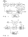
- a disk 1 is driven at a constant linear velocity (CLV) by means of a motor 8, and an optical pickup (PU) 2 including a semiconductor laser, a photoelectric transducer, etc. (not shown) reads data recorded on the disk 1.
- the PU 2 outputs data as a current signal and supplies it to a wide-band amplifier 3.
- the amplifier 3 amplifies the data and outputs an RF signal as a voltage signal.
- the RF signal is supplied to a data slice circuit 4.
- the data slice circuit 4 binarizes the RF signal and converts it into an EFM signal.
- the EFM signal is sent to a data processing circuit 6 and a PLL circuit 5.
- the PLL circuit 5 generates a PLL clock signal (PLCK) in synchronization with the EFM signal.
- the center frequency (17.2872 MHz) of the PLCK is four times as high as the bit rate (4.3218 MHz) of the EFM signal.
- the frequency of the PLCK is proportionate to a reproduction speed.
- the PLCK is supplied to the data processing circuit, together with the EFM signal.
- the PLCK is also supplied to the data slice circuit 4, and the control frequency band of a reference voltage can thus be controlled in accordance with the reproduction speed.
- the data processing circuit 6 executes EFM modulation, subcode modulation, error correction processing and the like, and an output signal thereof is supplied to a D/A converter (not shown).
- the output of the D/A converter is sent to a low-pass filter (not shown), and an audio signal is output from the low-pass filter.
- the data processing circuit 6 generates a system reference clock signal (XCK) using a quartz oscillator (not shown).
- a motor control circuit 7 control the motor 8 in response to the XCK supplied from the data processing circuit 6 in order to keep the reproduction speed constant.
- the reproduction speed is varied by a reproduction speed control signal (HS signal) supplied from a system controller 9. More specifically, the system controller 9 sets the HS signal to an equal speed, a two-times higher speed, a four-times higher speed, etc. in accordance with the normal reproduction or fast-forward reproduction designated by an operator, or the reproduction position of the disk.
- the HS signal is supplied to the processing circuit 6 and motor control circuit 7, and these circuits change the processing speed and the rotation speed of the disk in response to the HS signal.
- FIG. 2 schematically shows the data processing circuit 6.
- the EFM signal output from the data slice circuit 4 is supplied to an EFM demodulator 61 and demodulated therein.
- the output data of the EFM demodulator 61 is supplied to both a subcode demodulator 62 and a controller 63.
- the sub-code demodulator 62 separates the data into word components of 32 symbols including parity symbols P and Q and subcode data components.
- the controller 63 is connected to a RAM (random-access memory) 64.
- the RAM 64 is supplied with a clock signal CK1 for wiring data and a clock signal CK2 for reading data. These clock signals CK1 and CK2 are both generated from the foregoing PLL clock signal (PLCK).
- the controller 63 writes the data output from the EFM demodulator 61 to the RAM in response to the clock signal CK1 and reads the data written to the RAM 64 in response to the clock signal CK2. Consequently, a jitter due to the motor, contained in the data output from the EFM demodulator 61, is absorbed.
- the data read out from the RAM 64 is supplied to an error correction unit 65.
- the error correction unit 65 executes a C1-sequence error correction processing for data components of 32 symbols per frame, based on a parity symbol P, and then executes a de-interleave processing for data of 24 symbols and a parity symbol Q of 4 symbols.
- a CIRC cross interleave reed-solomon code
- a C2-sequence error correction processing based on the parity symbol Q. For example, an average of uncorrectable data is revised on the basis of the result of the error correction processing, and the revised average is output as 16-bit digital data.
- the 16-bit digital data is supplied to the D/A converter (not shown) and converted into an analog signal therein.
- the output signal of the D/A converter is supplied to a low-pass filter (not shown), and an audio signal is output from the low-pass filter.
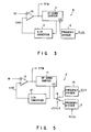
- FIG. 3 illustrates an example of the data slice circuit 4 described above.
- the RF signal output from the amplifier 3 is supplied to a non-inverting input terminal of a comparator 10, and a reference voltage Vref is supplied to an inverting input terminal thereof.
- the comparator 10 compares the RF signal and reference voltage Vref and converts the RF signal into binary data of "0" or "1".
- the output terminal of the comparator 10 is connected to an up-down counter 11.
- the up-down counter 11 is supplied with a clock signal CK to be counted.
- the up-down counter 11 counts the clock signal CK in accordance with a time period of data "0" output from the comparator 10 and that of data "1” output therefrom, and outputs differential data indicative of a difference between the time periods.
- the up-down counter 11 counts down the clock signal CK when data "0" is supplied from the comparator 10, and counts it up when data "1” is supplied therefrom. Therefore, the up-down counter 11 outputs the differential data.
- the differential data is supplied to a D/A converter 12, and converted into an analog voltage therein.
- the analog voltage is fed back to the comparator 10 as the reference voltage Vref mentioned above. This feedback causes the time periods of data "0” and data "1” output from the comparator 10 to be equalized to each other.
- the data "0" and "1” constitute an EFM signal.
- the clock signal CK supplied to the up-down counter 11 has a frequency which optimizes the control frequency band of the reference voltage Vref, and its frequency is 1/N times as high as that of the PLCK, the frequency of the CK being obtained by dividing the frequency of the PLCK by a frequency divider 13.
- the frequency of the clock signal CK varies in proportion to the reproduction speed if the PLL circuit 5 is locked by the EFM signal.
- the control frequency band of the reference voltage Vref of the data slice circuit 4 is therefore controlled in response to the reproduction speed.
- the PLL circuit 5 follows the speed, and the frequency of the PLCK increases. Since the frequency of the clock signal CK of the up-down counter 11 increases accordingly, the counting results vary rapidly and the transmission gain of the up-down counter 11 increases. Consequently, in a feedback loop, the open loop gain increases and the control frequency band broadens. If the reproduction speed decreases to the contrary, the frequency of the PLCK lowers and the control frequency band narrows.
- the controller 63 writes the output data of the EFM demodulator 61 to the RAM 64 in response to the clock signal CK1 generated from the PLCK and reads the output data from the RAM 64 in response to the clock signal CK2 generated from the PLCK.
- the error correction unit 65 executes an error correction processing in response to the PLL clock signal (PLCK). Therefore, data can be output immediately even when the reproduction speed is changed.
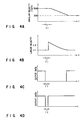
- the pickup 2 moves from the inner circumference of a disk to the outer circumference thereof during a period of time t1 when the outer circumference of the disk rotating at an angular velocity of 200 rpm is accessed after the inner circumference of the disk rotating at an angular velocity of 500 rpm.
- a PLL clock signal (PLCK) is used in the data processing circuit when data is written to the RAM, and a quartz reference clock signal (XCLK) is used therein when data is read out from the RAM. Moreover, the XCLK is employed in the error correction unit. For this reason, as shown in FIG. 4C, data cannot be stably reproduced before the linear velocity becomes an equal speed, and therefore the reproduction of data is intermitted.
- the data slice circuit 4 controls the control frequency band of the reference voltage Vref in response to the PLCK, the optimum control frequency band can be secured in accordance with the reproduction speed, and thus the same performance can be maintained for every reproduction speed.
- FIG. 5 shows another example of the data slice circuit 4.
- the same components as those of FIG. 3 are denoted by the same reference numerals, and their descriptions are omitted.
- the output signal of the frequency divider 13 is defined as the clock signal CK of the up-down counter 11.
- the data slice circuit shown in FIG. 5 includes a frequency divider 15 and a switch 16 in addition to the frequency divider 13. As described above, the frequency divider 13 generates a PLL type clock signal CK, by dividing the PLCK into 1/N.
- the frequency divider 15 generates a quartz type clock signal CK having a fixed frequency, by dividing the system reference clock signal XCK into 1/M.
- the switch 6 selects one of the clock signal CK output from the frequency divider 13 and the clock signal CK output from the frequency divider 15, in response to, for example, a lock/unlock signal (LS/ULS) output from the data processing circuit 6, and supplies the selected one to the up-down counter 11.
- LS/ULS lock/unlock signal
- a 24-bit frame synchronization signal is detected every 7.35 KHz in the data processing circuit 6 when the PLL circuit 5 is locked, and a detection cycle thereof varies when it is not locked.
- the switch 16 selects a PLL type clock signal CK output from the frequency divider 13.
- the switch 16 selects a quartz type clock signal CK output from the frequency divider 15.
- the frequency of the quartz type clock signal CK is set so as to optimize the control frequency band when the reproduction speed is at the middle of a range of variations thereof. If, therefore, the lock of the PLL circuit 5 is delayed by some factors, the control frequency band of the data slice circuit 4 can be prevented from being greatly shifted from the optimum value.
- the switching of the switch 16 is not limited to the case where the PLL circuit 5 is completely locked or unlocked, but can be executed in a range slightly shifted from the locked or unlocked state of the PLL circuit 5.
- the switching conditions of the switch 16 are as follows:
Landscapes
- Engineering & Computer Science (AREA)
- Signal Processing (AREA)
- Signal Processing For Digital Recording And Reproducing (AREA)
- Rotational Drive Of Disk (AREA)
Claims (12)
- Vorrichtung zur Verwendung bei der Diskdatenwiedergabe, wobei die Diskdaten von einer Disk gelesen werden und in ein verstärktes elektrisches Signal umgewandelt werden, wobei die Vorrichtung umfaßt:gekennzeichnet durch:eine Datenabtrennschaltung (4) zum Digitalisieren des verstärkten elektrischen Signals, um ein moduliertes Signal zu erzeugen;wobei die Datenabtrennschaltung (4) umfaßt:einen Vergleicher (10) zum Vergleichen des verstärkten elektrischen Signals mit einer Referenzspannung, wobei der Vergleicher (10) entweder einen Datenwert "0" oder einen Datenwert "1" in Abhängigkeit von dem verstärkten elektrischen Signal und der Referenzspannung ausgibt;eine Erfassungseinrichtung (11) zum Erfassen einer Differenz zwischen der Zeitperiode des Datenwerts "0" und der Zeitperiode des Datenwerts "1", und zum Erzeugen von differentiellen Daten, die die Differenz darstellen; undeine Spannungserzeugungseinrichtung (12), die die differentiellen Daten von der Erfassungseinrichtung (11) erhält, wobei die Spannungserzeugungseinrichtung (12) im Ansprechen auf die differentiellen Daten eine Spannung erzeugt und die Spannung an den Vergleicher (10) als die Referenzspannung führt;eine PLL-Schaltung (5) zum Erzeugen eines PLL-Taktsignals, das einer Änderung der Wiedergabegeschwindigkeit von Daten entspricht, im Ansprechen auf das modulierte Signal, das von der Datenabtrennschaltung (4) zugeführt wird; unddadurch, daß die Erfassungseinrichtung (11) die differentiellen Daten auf Grundlage eines Zählwerts des PLL-Taktsignals, zugeführt von der PLL-Schaltung (5), erzeugt.
- Vorrichtung nach Anspruch 1,
dadurch gekennzeichnet, daß die Erfassungseinrichtung (11) einen Aufwärts/Abwärts-Zähler umfaßt, der die differentiellen Daten durch Zählen des PLL-Taktsignals im Ansprechen auf die Zeitperiode des Datenwerts "0" und der Zeitperiode des Datenwerts "1" ausgibt. - Vorrichtung nach Anspruch 1,
dadurch gekennzeichnet, daß die
Spannungserzeugungseinrichtung (12) einen Digital-zu-Analog-Wandler umfaßt, der die diffentiellen Daten in eine analoge Spannung umwandelt und die analoge Spannung an den Vergleicher (10) als die Referenzspannung führt. - Vorrichtung nach Anspruch 1,
dadurch gekennzeichnet, daß die Datenabtrennschaltung (4) umfaßt:einen Frequenzteiler (13) zum Teilen einer Frequenz des von der PLL-Schaltung (5) zugeführten PLL-Taktsignals, um ein Zähltaktsignal zu erzeugen;einen Aufwärts/Abwärts-Zähler (11) zum Zählen des von dem Frequenzteiler (13) zugeführten Zähltaktsignals in Abhängigkeit von einer ersten Zeitperiode und des Datenwerts "0" und einer zweiten Zeitperiode des Datenwerts "1", die von dem Vergleicher "10" zugeführt wird, wobei der Aufwärts/Abwärts-Zähler (11) differentielle Daten ausgibt, die eine Differenz zwischen der ersten Zeitperiode des Datenwerts "0" und der zweiten Zeitperiode des Datenwerts "1" darstellen; undeinen Digital-zu-Analog-Wandler (12), an den die differentiellen Daten von dem Aufwärts/Abwärts-Zähler (11) geführt werden, wobei der Digital-zu-Analog-Wandler (12) die differentiellen Daten in eine analoge Spannung umwandelt und die analoge Spannung an den Vergleicher (10) als die Referenzspannung führt;wobei die Datenabtrennschaltung (4) betreibbar ist, um das verstärkte elektrische Signal in Abhängigkeit von der Änderung der Wiedergabegeschwindigkeit von Daten zu digitalisieren. - Vorrichtung nach Anspruch 4,
gekennzeichnet dadurch, daß sie eine
Datenverarbeitungsschaltung (6) zum Demodulieren des modulierten Signals, das von der Datenabtrennschaltung (4) zugeführt wird, im Ansprechen auf das von der PLL-Schaltung (5) zugeführte PLL-Taktsignal und zum Wiedergeben von Daten umfaßt. - Vorrichtung nach Anspruch 5,
dadurch gekennzeichnet, daß die Datenabtrennschaltung (6) umfaßt:einen ersten Demodulator (61) zum Demodulieren des modulierten Signals, das von der Datenabtrennschaltung (4) zugeführt wird;einen Speicher (64) zum Speichern von Daten, die von dem ersten Demodulator (61) ausgegeben werden;eine Steuereinrichtung (63) zum Schreiben der Daten, die von dem ersten Demodulator (61) ausgegeben werden, in den Speicher (64) im Ansprechen auf das von der PLL-Schaltung (5) zugeführte PLL-Taktsignal, und zum Auslesen der in den Speicher (64) geschriebenen Daten im Ansprechen auf das PLL-Taktsignal; undeine Fehlerkorrekturschaltung (65) zum Korrigieren eines Fehlers der von der Steuereinrichtung (63) ausgelesenen Daten im Ansprechen auf das von der PLL-Schaltung (5) zugeführte PLL-Taktsignal. - Vorrichtung nach Anspruch 6, ferner gekennzeichnet dadurch, daß sie einen zweiten Demodulator (62) zum Demodulieren der Datenausgabe von dem ersten Demodulator (61) in Untercode-Daten umfaßt.
- Vorrichtung nach Anspruch 1,
dadurch gekennzeichnet, daß die Datenabtrennschaltung (4) umfaßt:einen ersten Frequenzteiler (13) zum Teilen einer Frequenz des von der PLL-Schaltung (5) zugeführten PLL-Taktsignals und zum Erzeugen eines ersten Taktsignals;einen zweiten Frequenzteiler (15) zum Teilen einer Frequenz eines von einem Quarzoszillator zugeführten Referenztaktsignals und zum Ausgeben eines zweiten Taktsignals;einen Schalter (16), der mit den ersten und zweiten Frequenzteilern (13, 15) verbunden ist, zum Wählen entweder des ersten oder des zweiten Taktsignals und zum Ausgeben eines Wähltaktsignals;einen Aufwärts/Abwärts-Zähler (11) zum Zählen des von dem Schalter (16) zugeführten Zähltaktsignals in Abhängigkeit von einer ersten Zeitperiode des Datenwerts "0" und einer zweiten Zeitperiode des Datenwerts "1", die von dem Vergleicher (10) zugeführt wird, wobei der Aufwärts/Abwärts-Zähler (11) differentielle Daten ausgibt, die eine Differenz zwischen der ersten Zeitperiode des Datenwerts "0" und der zweiten Zeitperiode des Datenwerts "1" darstellen; undeinen Digital-zu-Analog-Wandler (12), an den die differentiellen Daten von dem Aufwärts/Abwärts-Zähler (11) geführt werden, wobei der Digital-zu-Analog-Wandler (12) die differentiellen Daten in eine analoge Spannung umwandelt und die analoge Spannung an den Vergleicher (10) als die Referenzspannung führt;wodurch die Datenabtrennschaltung (4) betreibbar ist, um das verstärkte elektrische Signal in Abhängigkeit von der Änderung der Wiedergabegeschwindigkeit der Daten zu digitalisieren. - Vorrichtung nach Anspruch 8,
dadurch gekennzeichnet, daß der Schalter (16) durch ein Steuersignal gesteuert wird, welches darstellt, ob die PLL-Schaltung (5) eingerastet ist oder nicht. - Vorrichtung nach Anspruch 9,
dadurch gekennzeichnet, daß der Schalter (16) das erste Taktsignal wählt, wenn das Steuersignal einen eingerasteten Zustand der PLL-Schaltung (5) darstellt, und der Schalter (16) das zweite Taktsignal wählt, wenn das Steuersignal einen nicht-eingerasteten Zustand der PLL-Schaltung (5) darstellt. - Vorrichtung nach Anspruch 9,
dadurch gekennzeichnet, daß der Schalter (16) das erste Taktsignal, das von der PLL-Schaltung (5) ausgegeben wird, wählt, wenn eine Frequenz des PLL-Taktsignals in einen vorgegebenen Frequenzbereich des modulierten Signals fällt, und der Schalter (16) das zweite Taktsignal wählt, wenn die Frequenz des PLL-Taktsignals außerhalb des vorgegebenen Frequenzbereichs des modulierten Signals fällt. - Vorrichtung nach einem der Ansprüche 2, 3, 4 und 8,
ferner gekennzeichnet dadurch, daß sie umfaßt:eine Aufnahmeeinrichtung (2) zum Lesen der Diskdaten und zum Umwandeln der Diskdaten in das verstärkte elektrische Signal; undeinen Motor (8) zum Drehen der Disk.
Applications Claiming Priority (6)
| Application Number | Priority Date | Filing Date | Title |
|---|---|---|---|
| JP305861/93 | 1993-11-11 | ||
| JP30586193 | 1993-11-11 | ||
| JP30586193 | 1993-11-11 | ||
| JP26276394 | 1994-10-26 | ||
| JP6262763A JP2885650B2 (ja) | 1993-11-11 | 1994-10-26 | ディスク再生装置 |
| JP262763/94 | 1994-10-26 |
Publications (3)
| Publication Number | Publication Date |
|---|---|
| EP0653753A2 EP0653753A2 (de) | 1995-05-17 |
| EP0653753A3 EP0653753A3 (de) | 1995-10-18 |
| EP0653753B1 true EP0653753B1 (de) | 1999-09-01 |
Family
ID=26545698
Family Applications (1)
| Application Number | Title | Priority Date | Filing Date |
|---|---|---|---|
| EP94117759A Expired - Lifetime EP0653753B1 (de) | 1993-11-11 | 1994-11-10 | Plattenwiedergabegerät mit Fähigkeit zur kontinuierlichen Änderung der Wiedergabegeschwindigkeit |
Country Status (5)
| Country | Link |
|---|---|
| US (2) | US5526339A (de) |
| EP (1) | EP0653753B1 (de) |
| JP (1) | JP2885650B2 (de) |
| KR (1) | KR0150493B1 (de) |
| DE (1) | DE69420359T2 (de) |
Families Citing this family (29)
| Publication number | Priority date | Publication date | Assignee | Title |
|---|---|---|---|---|
| JP3059860B2 (ja) * | 1993-07-07 | 2000-07-04 | 三洋電機株式会社 | ディスクプレーヤ |
| JP3594374B2 (ja) * | 1995-09-29 | 2004-11-24 | 松下電器産業株式会社 | ナビゲーション装置 |
| JP4112644B2 (ja) | 1996-02-28 | 2008-07-02 | パイオニア株式会社 | 情報記録媒体、情報記録装置及び情報記録方法並びに情報再生装置及び情報再生方法 |
| JPH09274770A (ja) * | 1996-04-03 | 1997-10-21 | Matsushita Electric Ind Co Ltd | 光ディスク再生装置及び再生方法 |
| USRE39491E1 (en) * | 1996-05-16 | 2007-02-20 | Sanyo Electric Co., Ltd. | Optical disk vibration sensing and reproducing device |
| US5886966A (en) * | 1996-05-16 | 1999-03-23 | Sanyo Electric Co., Ltd. | Optical disk vibration sensing and reproducing device |
| US6009053A (en) * | 1996-05-16 | 1999-12-28 | Tottori Sanyo Electric Co., Ltd. | Optical disk vibration sensing and reproducing device |
| JP3363712B2 (ja) | 1996-08-06 | 2003-01-08 | 株式会社リコー | 光ディスク装置 |
| DE19715274A1 (de) | 1997-04-12 | 1998-10-15 | Thomson Brandt Gmbh | Gerät zum Lesen und/oder Beschreiben optischer Aufzeichnungsträger |
| JP3607048B2 (ja) * | 1997-06-26 | 2005-01-05 | 株式会社東芝 | ディスク再生装置及びデータスライス回路 |
| JPH1116293A (ja) * | 1997-06-26 | 1999-01-22 | Toshiba Corp | 電圧制御発振回路及びディスク再生装置 |
| US7246897B2 (en) * | 1997-07-15 | 2007-07-24 | Silverbrook Research Pty Ltd | Media cartridge for inkjet printhead |
| KR19990024305A (ko) * | 1997-08-20 | 1999-04-06 | 윤종용 | 디지털 비디오 디스크 램의 데이터 슬라이스회로 |
| WO1999044196A1 (en) | 1998-02-27 | 1999-09-02 | Doug Carson & Associates, Inc. | Individual adjustment of pit and land transition locations in an optical disc mastering process |
| JP3916769B2 (ja) | 1998-06-02 | 2007-05-23 | 株式会社東芝 | ディスク再生装置及びディスク再生制御回路 |
| JP3528692B2 (ja) * | 1999-07-30 | 2004-05-17 | 株式会社日立製作所 | 情報記録再生装置、レーザドライバ、および、レーザドライバの駆動方法 |
| DE19961440A1 (de) | 1999-12-20 | 2001-06-21 | Thomson Brandt Gmbh | Gerät zum Lesen und/oder Schreiben optischer Aufzeichnungsträger |
| JP3956582B2 (ja) * | 2000-05-30 | 2007-08-08 | ヤマハ株式会社 | A/d変換回路 |
| JP3946421B2 (ja) * | 2000-08-04 | 2007-07-18 | 株式会社リコー | 光ディスク装置 |
| US7568081B2 (en) * | 2000-11-15 | 2009-07-28 | Doug Carson & Associates, Inc. | Authenticating a data storage medium using predetermined inter-sector relationships |
| US6477124B2 (en) | 2000-11-15 | 2002-11-05 | Doug Carson & Associates, Inc. | Varying the rate at which data appear on an optical disc rotated at a constant linear velocity to prevent unauthorized duplication of the disc |
| JP2002157841A (ja) * | 2000-11-16 | 2002-05-31 | Matsushita Electric Ind Co Ltd | ディスク再生装置のクロック抽出装置 |
| JP2002175674A (ja) * | 2000-12-05 | 2002-06-21 | Sony Corp | フェイズロックドループ回路 |
| US7627230B2 (en) | 2003-03-31 | 2009-12-01 | Samsung Electronics Co., Ltd. | Information storage medium containing enhanced AV (ENAV) buffer configuration information, reproducing method thereof and method for managing the buffer |
| US7274645B2 (en) * | 2003-06-10 | 2007-09-25 | Matsushita Electric Industrial Co., Ltd. | Reproduction signal processing apparatus and optical disc player including the same |
| KR100599128B1 (ko) * | 2004-07-08 | 2006-07-12 | 삼성전자주식회사 | 광디스크 재생장치 및 그의 최적 재생속도 결정방법 |
| JP4317826B2 (ja) * | 2005-03-10 | 2009-08-19 | パナソニック株式会社 | ジッタ検出装置 |
| US20080136468A1 (en) * | 2006-12-06 | 2008-06-12 | Dandan Li | Method and system for doubling phase-frequency detector comparison frequency for a fractional-n pll |
| TWI560965B (en) * | 2015-07-16 | 2016-12-01 | Actron Technology Corp | De-glitch circuit and de-glitch method and short circuit protection device |
Family Cites Families (13)
| Publication number | Priority date | Publication date | Assignee | Title |
|---|---|---|---|---|
| US3845500A (en) * | 1973-11-12 | 1974-10-29 | Ibm | Head to track alignment in a rotating head magnetic tape unit |
| JPS5539478A (en) * | 1978-09-14 | 1980-03-19 | Sony Corp | Regenerator of video signal |
| EP0077075B1 (de) * | 1981-10-14 | 1986-07-16 | Hitachi, Ltd. | Digitales Abspielgerät zum Reproduzieren einer digitalen Signalfolge |
| US5410527A (en) * | 1985-05-14 | 1995-04-25 | Canon Kabushiki Kaisha | Information recording/reproducing apparatus including setting optimum recording condition or reproducing condition |
| JPS62172567A (ja) * | 1986-01-24 | 1987-07-29 | Toshiba Corp | デイスク再生装置 |
| EP0289004B1 (de) * | 1987-04-28 | 1994-03-23 | Sharp Kabushiki Kaisha | Aufzeichnungs- und Wiedergabegerät |
| JPH03171437A (ja) * | 1989-11-30 | 1991-07-24 | Matsushita Electric Ind Co Ltd | 信号記録方法と最適パワー設定装置 |
| JP2915098B2 (ja) * | 1990-06-29 | 1999-07-05 | 株式会社日立製作所 | ディジタル信号記録再生装置 |
| US5418770A (en) * | 1990-06-29 | 1995-05-23 | Hitachi, Ltd. | Method of and apparatus for correcting edge interval of pit in optical recording/read-out apparatus |
| JP2807362B2 (ja) * | 1991-09-30 | 1998-10-08 | 株式会社東芝 | 情報再生装置 |
| JP3039056B2 (ja) * | 1991-11-25 | 2000-05-08 | ソニー株式会社 | 追記型光ディスク記録装置 |
| JP2920034B2 (ja) * | 1992-12-28 | 1999-07-19 | 株式会社東芝 | ディスク再生装置及び信号処理回路 |
| JP2830776B2 (ja) * | 1995-05-26 | 1998-12-02 | 日本電気株式会社 | 高密度記録向けクロック抽出方式 |
-
1994
- 1994-10-26 JP JP6262763A patent/JP2885650B2/ja not_active Expired - Fee Related
- 1994-11-10 EP EP94117759A patent/EP0653753B1/de not_active Expired - Lifetime
- 1994-11-10 DE DE69420359T patent/DE69420359T2/de not_active Expired - Lifetime
- 1994-11-11 KR KR1019940029562A patent/KR0150493B1/ko not_active Expired - Fee Related
-
1995
- 1995-08-07 US US08/512,076 patent/US5526339A/en not_active Ceased
-
1998
- 1998-06-10 US US09/100,779 patent/USRE36933E/en not_active Expired - Lifetime
Also Published As
| Publication number | Publication date |
|---|---|
| JP2885650B2 (ja) | 1999-04-26 |
| KR950015321A (ko) | 1995-06-16 |
| EP0653753A2 (de) | 1995-05-17 |
| US5526339A (en) | 1996-06-11 |
| DE69420359D1 (de) | 1999-10-07 |
| DE69420359T2 (de) | 2000-01-13 |
| EP0653753A3 (de) | 1995-10-18 |
| USRE36933E (en) | 2000-10-31 |
| JPH07182796A (ja) | 1995-07-21 |
| KR0150493B1 (ko) | 1998-10-15 |
Similar Documents
| Publication | Publication Date | Title |
|---|---|---|
| EP0653753B1 (de) | Plattenwiedergabegerät mit Fähigkeit zur kontinuierlichen Änderung der Wiedergabegeschwindigkeit | |
| EP0049136B1 (de) | Drehzahl-Kontrolleinrichtung für eine Speicherplatte | |
| EP0096106B1 (de) | PLL-Steuerkreis | |
| EP0098349B1 (de) | Frequenzdetektorschaltung für ein digitales Informationswiedergabesystem | |
| GB2062905A (en) | Disc record reproducing apparatuses | |
| JP2920034B2 (ja) | ディスク再生装置及び信号処理回路 | |
| EP0553851A2 (de) | Datenwiedergabegerät | |
| US6157603A (en) | Disk reproduction apparatus capable of continuously varying a reproduction speed | |
| US6359949B1 (en) | Demodulation circuit, a decode circuit and a digital PLL circuit for an optical disc apparatus | |
| EP0722169B1 (de) | Verfahren zur Wiedergabe | |
| JPH0877691A (ja) | ディスク再生装置及び信号処理回路 | |
| WO2004095454A1 (ja) | 再生装置および方法 | |
| JPS60171680A (ja) | デイジタルオ−デイオデイスク再生装置 | |
| JPH07134873A (ja) | ディスク再生装置及び信号処理回路 | |
| JPH1125588A (ja) | ディスクモータ制御回路及びこれを用いたディスク再生装置 | |
| JPH07141781A (ja) | データ再生用pll回路の制御装置 | |
| JP2002150696A (ja) | 再生装置 | |
| JPS6275972A (ja) | デイスクモ−タ制御回路 | |
| JPH0450673B2 (de) | ||
| JPH11296856A (ja) | 光ディスク再生方法および装置 | |
| JPS6252379B2 (de) | ||
| HK1015518A (en) | A demodulation circuit, a decode circuit and a digital pll circuit for an optical disc apparatus | |
| JPS58220225A (ja) | 位相ロツクル−プ制御回路 | |
| JPS6344359A (ja) | デジタルデ−タ再生装置におけるバツフアメモリのアドレス制御回路 |
Legal Events
| Date | Code | Title | Description |
|---|---|---|---|
| PUAI | Public reference made under article 153(3) epc to a published international application that has entered the european phase |
Free format text: ORIGINAL CODE: 0009012 |
|
| 17P | Request for examination filed |
Effective date: 19941110 |
|
| AK | Designated contracting states |
Kind code of ref document: A2 Designated state(s): DE FR GB |
|
| PUAL | Search report despatched |
Free format text: ORIGINAL CODE: 0009013 |
|
| AK | Designated contracting states |
Kind code of ref document: A3 Designated state(s): DE FR GB |
|
| GRAG | Despatch of communication of intention to grant |
Free format text: ORIGINAL CODE: EPIDOS AGRA |
|
| 17Q | First examination report despatched |
Effective date: 19981218 |
|
| GRAG | Despatch of communication of intention to grant |
Free format text: ORIGINAL CODE: EPIDOS AGRA |
|
| GRAH | Despatch of communication of intention to grant a patent |
Free format text: ORIGINAL CODE: EPIDOS IGRA |
|
| GRAH | Despatch of communication of intention to grant a patent |
Free format text: ORIGINAL CODE: EPIDOS IGRA |
|
| GRAA | (expected) grant |
Free format text: ORIGINAL CODE: 0009210 |
|
| AK | Designated contracting states |
Kind code of ref document: B1 Designated state(s): DE FR GB |
|
| REF | Corresponds to: |
Ref document number: 69420359 Country of ref document: DE Date of ref document: 19991007 |
|
| PG25 | Lapsed in a contracting state [announced via postgrant information from national office to epo] |
Ref country code: GB Free format text: LAPSE BECAUSE OF NON-PAYMENT OF DUE FEES Effective date: 19991201 |
|
| ET | Fr: translation filed | ||
| PLBE | No opposition filed within time limit |
Free format text: ORIGINAL CODE: 0009261 |
|
| STAA | Information on the status of an ep patent application or granted ep patent |
Free format text: STATUS: NO OPPOSITION FILED WITHIN TIME LIMIT |
|
| GBPC | Gb: european patent ceased through non-payment of renewal fee |
Effective date: 19991201 |
|
| 26N | No opposition filed | ||
| PGFP | Annual fee paid to national office [announced via postgrant information from national office to epo] |
Ref country code: DE Payment date: 20101104 Year of fee payment: 17 |
|
| PGFP | Annual fee paid to national office [announced via postgrant information from national office to epo] |
Ref country code: FR Payment date: 20111118 Year of fee payment: 18 |
|
| REG | Reference to a national code |
Ref country code: FR Ref legal event code: ST Effective date: 20130731 |
|
| REG | Reference to a national code |
Ref country code: DE Ref legal event code: R119 Ref document number: 69420359 Country of ref document: DE Effective date: 20130601 |
|
| PG25 | Lapsed in a contracting state [announced via postgrant information from national office to epo] |
Ref country code: DE Free format text: LAPSE BECAUSE OF NON-PAYMENT OF DUE FEES Effective date: 20130601 |
|
| PG25 | Lapsed in a contracting state [announced via postgrant information from national office to epo] |
Ref country code: FR Free format text: LAPSE BECAUSE OF NON-PAYMENT OF DUE FEES Effective date: 20121130 |