EP0634465A1 - Methode zum Polieren einer Kupferoberfläche oder einer Legierung mit Kupfer als Hauptbestandteil - Google Patents
Methode zum Polieren einer Kupferoberfläche oder einer Legierung mit Kupfer als Hauptbestandteil Download PDFInfo
- Publication number
- EP0634465A1 EP0634465A1 EP94201956A EP94201956A EP0634465A1 EP 0634465 A1 EP0634465 A1 EP 0634465A1 EP 94201956 A EP94201956 A EP 94201956A EP 94201956 A EP94201956 A EP 94201956A EP 0634465 A1 EP0634465 A1 EP 0634465A1
- Authority
- EP
- European Patent Office
- Prior art keywords
- polishing
- copper
- volume
- units
- chemical activator
- Prior art date
- Legal status (The legal status is an assumption and is not a legal conclusion. Google has not performed a legal analysis and makes no representation as to the accuracy of the status listed.)
- Granted
Links
Images


Classifications
-
- C—CHEMISTRY; METALLURGY
- C09—DYES; PAINTS; POLISHES; NATURAL RESINS; ADHESIVES; COMPOSITIONS NOT OTHERWISE PROVIDED FOR; APPLICATIONS OF MATERIALS NOT OTHERWISE PROVIDED FOR
- C09G—POLISHING COMPOSITIONS; SKI WAXES
- C09G1/00—Polishing compositions
- C09G1/02—Polishing compositions containing abrasives or grinding agents
-
- C—CHEMISTRY; METALLURGY
- C09—DYES; PAINTS; POLISHES; NATURAL RESINS; ADHESIVES; COMPOSITIONS NOT OTHERWISE PROVIDED FOR; APPLICATIONS OF MATERIALS NOT OTHERWISE PROVIDED FOR
- C09K—MATERIALS FOR MISCELLANEOUS APPLICATIONS, NOT PROVIDED FOR ELSEWHERE
- C09K3/00—Materials not provided for elsewhere
- C09K3/14—Anti-slip materials; Abrasives
- C09K3/1454—Abrasive powders, suspensions and pastes for polishing
- C09K3/1463—Aqueous liquid suspensions
-
- G—PHYSICS
- G11—INFORMATION STORAGE
- G11B—INFORMATION STORAGE BASED ON RELATIVE MOVEMENT BETWEEN RECORD CARRIER AND TRANSDUCER
- G11B5/00—Recording by magnetisation or demagnetisation of a record carrier; Reproducing by magnetic means; Record carriers therefor
- G11B5/127—Structure or manufacture of heads, e.g. inductive
- G11B5/31—Structure or manufacture of heads, e.g. inductive using thin films
- G11B5/3163—Fabrication methods or processes specially adapted for a particular head structure, e.g. using base layers for electroplating, using functional layers for masking, using energy or particle beams for shaping the structure or modifying the properties of the basic layers
Definitions
- the invention relates to a method of polishing a surface of copper or an alloy comprising mainly copper, in which a polishing means and said surface are moved with respect to each other while exerting a polishing pressure for obtaining a polished surface.
- the method according to the invention is characterized in that a composition of a polishing component comprising a colloidal suspension of SiO2 particles having an average particle size of between 20 and 50 nm in an alkali solution, demineralised water and a chemical activator is used as a polishing means, while a polishing pressure of between 400 and 600 g/cm2 is exerted by means of a polishing base absorbing a polishing means, which polishing base has a hardness in the range between Shore A hardness 40 and Shore D hardness 90.
- the Shore A and D hardnesses are defined in DIN 53505.
- the method according to the invention for copper or alloys comprising mainly copper such as brass or bronze yield substantially plane polished surfaces without defects, with surface roughnesses R (rms) of less than 2 nm being achievable. It is assumed that the particles used have an optimum size and hardness for polishing copper and copper alloys without damaging the material structure.
- the chemical activator is used for optimizing oxidation. Physical, chemical and mechanical parameters play a role in the method according to the invention.
- the polishing pressure is an external magnitude with which the method can be controlled and optimized.
- polishing pressure yields an optimum result because a lower pressure is a too great advantage for the chemical aspect ad yields a slightly rough surface, while a higher pressure is a too great advantage for the mechanical aspect, which in turn also results in a rougher surface.
- the polishing base retains the polishing means during polishing and thus ensures, inter alia an optimum wetting of the surface to be polished.
- a tissue of organic fibres or a polishing cloth of pressed organic fibres is preferably used. The hardness of the polishing base is extremely important for optimizing the method according to the invention.
- a mechano-chemical polishing means is known under the trade name of Syton which comprises SiO2 nanoparticles in a basic solution.
- Syton which comprises SiO2 nanoparticles in a basic solution.
- this means is not suitable for accurately polishing surfaces of copper or copper alloys.
- the above-mentioned means is mentioned, inter alia in US 3,485,608 (herewith incorporated by reference) which describes a method of polishing silicon wafers.
- An embodiment of the method according to the invention is characterized in that the polishing component comprises approximately 50% by weight of SiO2 particles and approximately 50% by weight of solution having a pH of approximately 10.
- the pH of approximately 10 is controlled by means of the alkaline addition whose concentration is approximately 10 ⁇ 4 molar.
- An embodiment of the method according to the invention is characterized in that 60 to 100 units by volume of demineralised water and 25 to 50 units by volume of chemical activator are used for every 100 units by volume of polishing component.
- relatively ductile materials such as copper
- coagulation of the polishing means should be prevented during the polishing operation, while there should still be a chemical effect.
- the degree of dilution as proposed in the method according to the invention complies with this.
- the aspect of the chemical effect may be further optimized.
- An embodiment of the method according to the invention is characterized in that a hydrogen peroxide, an organic peroxide or a hypochloride is used as a chemical activator.
- a chemical activator increases, for example by oxidation, the desorption of the material released during polishing and causes this material to dissolve. This is in contrast to the local plastic deformation of the material on the surface, as is the usual phenomenon in purely mechanical polishing methods.
- An embodiment of the method according to the invention is characterized in that the method starts from a substrate on which a layer having a surface of copper or an alloy comprising mainly copper is formed.
- This embodiment in which an electrically conducting layer may be structured, is particularly suitable for use in the manufacture of planar thin-film magnetic heads in which strict requirements as regards smoothness, planeness ad condition, particularly physical condition of polished surfaces are imposed.
- a structured layer formed as a write and/or test winding generally occurs.
- the layer should have a low resistance, for example less than 1 Ohm.
- the method according to the invention provides the possibility of using narrow, relatively thick windings, in which the layer is embedded in the substrate. A hard ferrite can be used without any problem as a substrate material.
- An embodiment of the method according to the invention is characterized in that a non-magnetic layer is deposited on the polished surface obtained for forming a transducing gap of a magnetic head. Due to the accurate polished surface which is present, the non-magnetic layer may be perfectly smooth without any thickness variations when using the method according to the invention and may thus have an accurately defined thickness. The thickness of the non-magnetic layer determines the writing behaviour of the magnetic head obtained. For example, SiO2 or ZrO2 may be used as a material for the non-magnetic layer, which material may be deposited by PE-CVD or sputtering, respectively. By using a recessed conductor, the thickness of the non-magnetic layer can also be chosen freely for a small write gap.
- thick insulation layers In the case of a non-recessed conductor, thick insulation layers must be provided so as to ensure satisfactory step coatings and to prevent short-circuits between the conductor and the magnetic yoke of the magnetic head, which thick insulation layers must be re-etched at a later stage to the correct thickness so as to realise the desired write gap.
- the invention also relates to a magnetic head obtainable by means of the method according to the invention.
- the thin-film magnetic head obtained may be a read and/or write head.
- a read head a high efficiency is required.
- a recess or a groove can be provided in a magnetic substrate when using the method according to the invention.
- Copper or an alloy comprising mainly copper is deposited in the recess so as to form an electric conductor, whereafter a planarization process is carried out, using the method according to the invention for obtaining a polished surface.
- the electric conductor is embedded in the magnetic substrate of the magnetic head thus obtained.
- the invention also relates to an X-ray radiation-collimating element having a surface polished by means of the method according to the invention.
- the invention also relates to a X-ray radiation-reflecting element having a surface polished by means of the method according to the invention.
- Said elements may be used, for example as elements limiting the radiation divergence and may function as a reference for surfaces. It is therefore important that said elements have a optimally defined surface quality.
- the invention further relates to a polishing means which is suitable for use in the method according to the invention.
- the polishing means according to the invention is characterized by the presence of a polishing component comprising a colloidal suspension of SiO2 particles having a average particle size of between 20 and 50 nm in a alkali solution, demineralised water and a chemical activator, in which 60 to 100 units by volume of demineralised water and 25 to 50 units by volume of chemical activator are present for every 100 units by volume of polishing component.
- the alkali solution may be KOH or NaOH.
- a practical embodiment of the polishing means according to the invention is characterized in that the polishing component comprises approximately 50% by weight of SiO2 particles, in which the solution has a pH of substantially 10.
- An embodiment of the polishing means according to the invention is characterized in that the chemical activator is a substance from the group formed by hydrogen peroxide, organic peroxides and hypochlorides. To optimize the chemical aspect of this method, viz . the dissolution of material released during polishing, addition of this chemical activator is necessary.
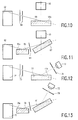
- a method of manufacturing a thin-film magnetic head, using an embodiment of the method according to the invention will be described with reference to Figs. 1 to 8.
- the method starts from a soft-magnetic substrate 1, in this embodiment a ferrite such as NiZn ferrite having a smooth ad plane substrate surface on which a mask 3, in this embodiment a mask of nickel is formed by successive deposition and structuring.
- the deposition of a nickel layer may be performed by means of an electroplating process, while a photoresist layer may be used for structuring.
- a groove or recess 1a is formed in the substrate 1 by removal of material, for example by sputter-etching or reactive ion etching, whereafter any remaining parts of the mask 3 are removed by, for example wet-chemical etching.
- a copper layer 5 is provided, for example, by means of sputtering on the substrate 1 thus structured.
- a layer of an adhesive material may be formed before copper is provided.
- the layer 5 has a copper surface 5a remote from the substrate 1, which surface is polished by means of the method according to the invention for obtaining a winding 7 serving as an inductive transducing element and having an at least substantially plane surface 7a without scratches and defects.
- an embodiment of the polishing means according to the invention is used, which in this example comprises 400 cc of polishing component, 400 cc of demineralised water and 160 cc of hydrogen peroxide.
- the polishing component comprises 50.4% by weight of SiO2 particles in water in which 10 ⁇ 4 molar of a base is added. The particles have an average size of 36 nm.
- the pH is 10.1.
- the polishing means is moved across the surface 5a by means of a polishing base of organic fibres having a Shore D hardness of approximately 35 while simultaneously exerting a polishing pressure of approximately 500 g/cm2. It has surprisingly been found that the polished copper surface 7a obtained perfectly adjoins the adjacent surface portions 1b of the substrate 1, in which height differences of less than 100 nm can easily be realised.
- the surfaces 1b and 7a jointly form a smooth main surface 9 on which a layer 11 of a non-magnetic, electrically non-conducting material is formed.
- a layer 11 of a non-magnetic, electrically non-conducting material is formed.
- quartz or zirconia can be deposited by means of PE-CVD or sputtering, respectively.
- the layer 11 has an accurate uniform layer thickness because a portion of the layer 11 in the manufactured magnetic head functions as a transducing gap 11a (see Fig. 9).
- connection aperture 13 is provided by means of a known technique, for example by chemical etching in the case of a quartz layer.
- a soft-magnetic material for example an NiFe alloy or a CoZrNb alloy is deposited by means of a known deposition technique for forming a flux-guiding layer 15.
- the layer 15 is polished for forming a flux guide 15a and a head face 17 can be formed by means of grinding and/or polishing.
- Fig. 9 shows a thin-film magnetic head obtained by means of the method described above.
- This magnetic head comprises an inductive element 7 of copper which is recessed in the substrate 1 and is provided with a magnetic yoke formed by the substrate 1 and the flux guide 15a and a non-magnetic transducing gap 11a.
- the method according to the invention is not limited to its use in processes of manufacturing magnetic heads, but is suitable for many applications in which strict requirements are imposed on the condition of copper surfaces or surfaces of alloys comprising mainly copper.
- the method may be used successfully, for example when manufacturing mirrors having a mirror surface of copper or a copper alloy.
- Such mirrors may be used, for example as X-ray radiation-collimating elements, as dispersive elements or as calibration samples in X-ray reflectometers.
- the polished surface obtained by means of the method according to the invention may be coated with a thin layer of, for example 30 nm, of a noble metal such as gold.
- the devices shown in Figs. 10 and 11 relate to glancing incidence X-ray analysis. Measurements can be performed with these devices for obtaining information about, inter alia layer thicknesses, interface roughnesses, lateral roughness correlations, composition profiles and thin-layer structures.
- the device shown in Fig. 10 comprises an energy-dispersive spectrometer 50, an X-ray tube 52 and transmission gaps 54 for limiting the divergence of an X-ray beam incident on a calibration sample 56.
- the pivotably adjusted sample 56 has a surface 56a polished by means of the method according to the invention.
- the device shown in Fig. 11 comprises an energy-dispersive spectrometer 60, an X-ray tube 62, a transmission gap 64 and a plane or curved mirror 65 for dispersive processing of an X-ray beam incident on a pivotable sample 67.
- the mirror 65 has a copper surface 65a polished by means of the method according to the invention.
- the devices shown in Figs. 12 and 13 are provided with an X-ray tube 71 ad a detector 73 each.
- the device of Fig. 12 also has transmission gaps 75 for limiting the divergence of X-ray radiation incident on a pivotable calibration sample 77, and a gap 78 in front of the detector which determines the acceptance angle of the radiation.
- the copper sample 77 has a surface 77a polished by means of the method according to the invention.
- the device of Fig. 13 has a mirror 79 for dispersive processing of radiation incident on a sample 81.
- the mirror 79 has a surface 79a obtained by means of the method according to the invention.
- the elements 65 and 79 in Figs. 11 and 13 may have either a reflecting or a collimating character, dependent on the curvature of the elements.
- the invention is not limited to the embodiments shown.
- successful experiments were performed with other embodiments of the polishing means according to the invention.
- the volume ratios between the polishing component, demineralised water and chemical activator were 100:100:25, 100:60:50 and 100:60:40, respectively.
Landscapes
- Chemical & Material Sciences (AREA)
- Organic Chemistry (AREA)
- Engineering & Computer Science (AREA)
- Materials Engineering (AREA)
- Manufacturing & Machinery (AREA)
- ing And Chemical Polishing (AREA)
- Finish Polishing, Edge Sharpening, And Grinding By Specific Grinding Devices (AREA)
- Grinding And Polishing Of Tertiary Curved Surfaces And Surfaces With Complex Shapes (AREA)
- Magnetic Heads (AREA)
Applications Claiming Priority (2)
| Application Number | Priority Date | Filing Date | Title |
|---|---|---|---|
| BE9300716A BE1007281A3 (nl) | 1993-07-12 | 1993-07-12 | Werkwijze voor het polijsten van een oppervlak van koper of een in hoofdzaak koper bevattende legering, magneetkop vervaardigbaar met gebruikmaking van de werkwijze, röntgenstralingcollimerend element en röntgenstralingreflecterend element, beide voorzien van een volgens de werkwijze gepolijst oppervlak en polijstmiddel geschikt voor toepassing in de werkwijze. |
| BE9300716 | 1993-07-12 |
Publications (2)
| Publication Number | Publication Date |
|---|---|
| EP0634465A1 true EP0634465A1 (de) | 1995-01-18 |
| EP0634465B1 EP0634465B1 (de) | 1998-11-11 |
Family
ID=3887173
Family Applications (1)
| Application Number | Title | Priority Date | Filing Date |
|---|---|---|---|
| EP94201956A Expired - Lifetime EP0634465B1 (de) | 1993-07-12 | 1994-07-07 | Methode zum Polieren einer Kupferoberfläche oder einer Legierung mit Kupfer als Hauptbestandteil |
Country Status (10)
| Country | Link |
|---|---|
| US (1) | US5622525A (de) |
| EP (1) | EP0634465B1 (de) |
| JP (1) | JPH0775943A (de) |
| BE (1) | BE1007281A3 (de) |
| DE (1) | DE69414480T2 (de) |
| HK (1) | HK1013093A1 (de) |
| HU (1) | HU217664B (de) |
| MY (1) | MY111523A (de) |
| SG (1) | SG48408A1 (de) |
| TW (1) | TW346503B (de) |
Cited By (3)
| Publication number | Priority date | Publication date | Assignee | Title |
|---|---|---|---|---|
| EP0823465A2 (de) * | 1996-08-06 | 1998-02-11 | Showa Denko Kabushiki Kaisha | Polierzusammensetzung zum chemisch-mechanischen Polieren |
| EP1211719A1 (de) * | 2000-12-04 | 2002-06-05 | Bayer Ag | Poliersuspension für das chemisch-mechanische Polieren von Metall- und Dielektrikastrukturen |
| US8092707B2 (en) | 1997-04-30 | 2012-01-10 | 3M Innovative Properties Company | Compositions and methods for modifying a surface suited for semiconductor fabrication |
Families Citing this family (22)
| Publication number | Priority date | Publication date | Assignee | Title |
|---|---|---|---|---|
| US20090255189A1 (en) * | 1998-08-19 | 2009-10-15 | Nanogram Corporation | Aluminum oxide particles |
| US20060147369A1 (en) * | 1997-07-21 | 2006-07-06 | Neophotonics Corporation | Nanoparticle production and corresponding structures |
| US20090075083A1 (en) * | 1997-07-21 | 2009-03-19 | Nanogram Corporation | Nanoparticle production and corresponding structures |
| JP3366256B2 (ja) * | 1998-07-02 | 2003-01-14 | アルプス電気株式会社 | 薄膜磁気ヘッド及びその製造方法 |
| FR2781922B1 (fr) * | 1998-07-31 | 2001-11-23 | Clariant France Sa | Procede de polissage mecano-chimique d'une couche en un materiau a base de cuivre |
| US6206756B1 (en) | 1998-11-10 | 2001-03-27 | Micron Technology, Inc. | Tungsten chemical-mechanical polishing process using a fixed abrasive polishing pad and a tungsten layer chemical-mechanical polishing solution specifically adapted for chemical-mechanical polishing with a fixed abrasive pad |
| US6276996B1 (en) * | 1998-11-10 | 2001-08-21 | Micron Technology, Inc. | Copper chemical-mechanical polishing process using a fixed abrasive polishing pad and a copper layer chemical-mechanical polishing solution specifically adapted for chemical-mechanical polishing with a fixed abrasive pad |
| US6589872B1 (en) * | 1999-05-03 | 2003-07-08 | Taiwan Semiconductor Manufacturing Company | Use of low-high slurry flow to eliminate copper line damages |
| US6375693B1 (en) | 1999-05-07 | 2002-04-23 | International Business Machines Corporation | Chemical-mechanical planarization of barriers or liners for copper metallurgy |
| JP2000338299A (ja) * | 1999-05-28 | 2000-12-08 | Mitsubishi Electric Corp | X線露光装置、x線露光方法、x線マスク、x線ミラー、シンクロトロン放射装置、シンクロトロン放射方法および半導体装置 |
| US6179691B1 (en) * | 1999-08-06 | 2001-01-30 | Taiwan Semiconductor Manufacturing Company | Method for endpoint detection for copper CMP |
| JP3492953B2 (ja) * | 1999-10-05 | 2004-02-03 | Tdk株式会社 | 薄膜磁気ヘッドの製造方法 |
| US6527817B1 (en) | 1999-11-15 | 2003-03-04 | Cabot Microelectronics Corporation | Composition and method for planarizing surfaces |
| US6319096B1 (en) | 1999-11-15 | 2001-11-20 | Cabot Corporation | Composition and method for planarizing surfaces |
| US6293848B1 (en) * | 1999-11-15 | 2001-09-25 | Cabot Microelectronics Corporation | Composition and method for planarizing surfaces |
| JP3499490B2 (ja) * | 2000-02-16 | 2004-02-23 | Tdk株式会社 | 薄膜磁気ヘッドの製造方法 |
| JP2002093684A (ja) | 2000-09-18 | 2002-03-29 | Canon Inc | X線露光装置、x線露光方法、半導体製造装置および微細構造体 |
| US6589100B2 (en) | 2001-09-24 | 2003-07-08 | Cabot Microelectronics Corporation | Rare earth salt/oxidizer-based CMP method |
| US7087529B2 (en) * | 2003-10-02 | 2006-08-08 | Amcol International Corporation | Chemical-mechanical polishing (CMP) slurry and method of planarizing surfaces |
| US7223156B2 (en) * | 2003-11-14 | 2007-05-29 | Amcol International Corporation | Method chemical-mechanical polishing and planarizing corundum, GaAs, GaP and GaAs/GaP alloy surfaces |
| EP1758962B1 (de) * | 2004-06-22 | 2013-10-30 | Asahi Glass Company, Limited | Polierverfahren für glassubstrat sowie glassubstrat |
| JP5897597B2 (ja) | 2010-12-08 | 2016-03-30 | ギャリオン インターナショナル コーポレイション | 硬質で低摩擦の金属窒化物被膜を形成する方法 |
Citations (4)
| Publication number | Priority date | Publication date | Assignee | Title |
|---|---|---|---|---|
| FR1441504A (fr) * | 1965-01-22 | 1966-06-10 | Monsanto Co | Procédé de polissage |
| US4358295A (en) * | 1980-03-27 | 1982-11-09 | Matsushita Electric Industrial Co., Ltd. | Polishing method |
| FR2574064A1 (fr) * | 1984-12-04 | 1986-06-06 | Mitsubishi Chem Ind | Dispersion aqueuse d'anhydride silicique et composition abrasive comprenant cette dispersion |
| US4959113A (en) * | 1989-07-31 | 1990-09-25 | Rodel, Inc. | Method and composition for polishing metal surfaces |
Family Cites Families (6)
| Publication number | Priority date | Publication date | Assignee | Title |
|---|---|---|---|---|
| US3485608A (en) * | 1968-01-02 | 1969-12-23 | Texas Instruments Inc | Slurry for polishing silicon slices |
| US3662500A (en) * | 1971-01-28 | 1972-05-16 | Ibm | Method for polishing magnetic oxide materials |
| US4057939A (en) * | 1975-12-05 | 1977-11-15 | International Business Machines Corporation | Silicon wafer polishing |
| EP0348757B1 (de) * | 1988-06-28 | 1995-01-04 | Mitsubishi Materials Silicon Corporation | Verfahren zur Polierung eines Halbleiter-Plättchens |
| US5352277A (en) * | 1988-12-12 | 1994-10-04 | E. I. Du Pont De Nemours & Company | Final polishing composition |
| US5230833A (en) * | 1989-06-09 | 1993-07-27 | Nalco Chemical Company | Low sodium, low metals silica polishing slurries |
-
1993
- 1993-07-12 BE BE9300716A patent/BE1007281A3/nl not_active IP Right Cessation
-
1994
- 1994-03-15 TW TW083102218A patent/TW346503B/zh active
- 1994-03-16 US US08/213,768 patent/US5622525A/en not_active Expired - Fee Related
- 1994-06-23 MY MYPI94001627A patent/MY111523A/en unknown
- 1994-07-06 HU HU9402034A patent/HU217664B/hu not_active IP Right Cessation
- 1994-07-07 EP EP94201956A patent/EP0634465B1/de not_active Expired - Lifetime
- 1994-07-07 SG SG1996009454A patent/SG48408A1/en unknown
- 1994-07-07 DE DE69414480T patent/DE69414480T2/de not_active Expired - Fee Related
- 1994-07-11 JP JP6158638A patent/JPH0775943A/ja active Pending
-
1998
- 1998-12-19 HK HK98114093A patent/HK1013093A1/xx not_active IP Right Cessation
Patent Citations (5)
| Publication number | Priority date | Publication date | Assignee | Title |
|---|---|---|---|---|
| FR1441504A (fr) * | 1965-01-22 | 1966-06-10 | Monsanto Co | Procédé de polissage |
| US4358295A (en) * | 1980-03-27 | 1982-11-09 | Matsushita Electric Industrial Co., Ltd. | Polishing method |
| FR2574064A1 (fr) * | 1984-12-04 | 1986-06-06 | Mitsubishi Chem Ind | Dispersion aqueuse d'anhydride silicique et composition abrasive comprenant cette dispersion |
| US4959113A (en) * | 1989-07-31 | 1990-09-25 | Rodel, Inc. | Method and composition for polishing metal surfaces |
| US4959113C1 (en) * | 1989-07-31 | 2001-03-13 | Rodel Inc | Method and composition for polishing metal surfaces |
Cited By (4)
| Publication number | Priority date | Publication date | Assignee | Title |
|---|---|---|---|---|
| EP0823465A2 (de) * | 1996-08-06 | 1998-02-11 | Showa Denko Kabushiki Kaisha | Polierzusammensetzung zum chemisch-mechanischen Polieren |
| EP0823465A3 (de) * | 1996-08-06 | 1998-10-21 | Showa Denko Kabushiki Kaisha | Polierzusammensetzung zum chemisch-mechanischen Polieren |
| US8092707B2 (en) | 1997-04-30 | 2012-01-10 | 3M Innovative Properties Company | Compositions and methods for modifying a surface suited for semiconductor fabrication |
| EP1211719A1 (de) * | 2000-12-04 | 2002-06-05 | Bayer Ag | Poliersuspension für das chemisch-mechanische Polieren von Metall- und Dielektrikastrukturen |
Also Published As
| Publication number | Publication date |
|---|---|
| HU9402034D0 (en) | 1994-09-28 |
| EP0634465B1 (de) | 1998-11-11 |
| MY111523A (en) | 2000-07-31 |
| JPH0775943A (ja) | 1995-03-20 |
| HK1013093A1 (en) | 1999-08-13 |
| TW346503B (en) | 1998-12-01 |
| BE1007281A3 (nl) | 1995-05-09 |
| HUT71054A (en) | 1995-11-28 |
| DE69414480T2 (de) | 1999-06-02 |
| SG48408A1 (en) | 1998-04-17 |
| HU217664B (hu) | 2000-03-28 |
| US5622525A (en) | 1997-04-22 |
| DE69414480D1 (de) | 1998-12-17 |
Similar Documents
| Publication | Publication Date | Title |
|---|---|---|
| US5622525A (en) | Method of polishing a surface of copper or an alloy comprising mainly copper | |
| US5531016A (en) | Method of manufacturing a thin-film magnetic head | |
| EP1526948B1 (de) | Durch magnetorheologische feinstbearbeitung hergestellte gleichförmige dünne filme | |
| US5483735A (en) | Method of manufacturing a thin-film magnetic head | |
| US5637028A (en) | Method of polishing a surface of a noble metal | |
| US6554878B1 (en) | Slurry for multi-material chemical mechanical polishing | |
| JP2000339658A (ja) | 磁気記録媒体、この製造方法及びこの媒体を用いた磁気記憶装置 | |
| CN100342428C (zh) | 用于浮动块测试器的换能头悬架组件 | |
| US5923511A (en) | Directly contactable disk for vertical magnetic data storage | |
| JP2006082138A (ja) | 磁気ディスク用ガラス基板の製造方法及び磁気ディスク用ガラス基板、並びに、磁気ディスクの製造方法及び磁気ディスク | |
| JP2737901B2 (ja) | 磁気ディスク用ガラス基板の製造方法 | |
| JPH1110492A (ja) | 磁気ディスク基板およびその製造方法 | |
| EP0617410B1 (de) | Herstellungsverfahren eines Dünnfilmmagnetkopfes und danach hergestellter Magnetkopf | |
| WO1998044541A1 (en) | Flattening process for semiconductor wafers | |
| JP2011134419A (ja) | 磁気記録媒体用ディスク基板及びその製造方法 | |
| Higashi et al. | New machining method for making precise and very smooth mirror surfaces made from Cu and Al alloys for synchrotron radiation optics | |
| JP3519927B2 (ja) | 磁気記録媒体用基板 | |
| US7514016B2 (en) | Methodology of chemical mechanical nanogrinding for ultra precision finishing of workpieces | |
| JPS6038720A (ja) | 磁気ディスク用基板 | |
| JP4411314B2 (ja) | 磁気記録媒体用シリコン基板およびその製造方法 | |
| JPH0451885B2 (de) | ||
| JP2009217870A (ja) | 磁気記録用シリコン基板およびその製造方法 | |
| EP0555906A1 (de) | Glasträger für magnetisches Aufzeichnungsmedium | |
| JPS6048253A (ja) | 結晶化ガラスの精密研摩方法 | |
| JP4023609B2 (ja) | 磁気記録媒体用基板及び磁気記録媒体の製造方法 |
Legal Events
| Date | Code | Title | Description |
|---|---|---|---|
| PUAI | Public reference made under article 153(3) epc to a published international application that has entered the european phase |
Free format text: ORIGINAL CODE: 0009012 |
|
| AK | Designated contracting states |
Kind code of ref document: A1 Designated state(s): DE FR GB IT |
|
| 17P | Request for examination filed |
Effective date: 19950718 |
|
| 17Q | First examination report despatched |
Effective date: 19961220 |
|
| GRAG | Despatch of communication of intention to grant |
Free format text: ORIGINAL CODE: EPIDOS AGRA |
|
| GRAG | Despatch of communication of intention to grant |
Free format text: ORIGINAL CODE: EPIDOS AGRA |
|
| GRAH | Despatch of communication of intention to grant a patent |
Free format text: ORIGINAL CODE: EPIDOS IGRA |
|
| GRAH | Despatch of communication of intention to grant a patent |
Free format text: ORIGINAL CODE: EPIDOS IGRA |
|
| GRAA | (expected) grant |
Free format text: ORIGINAL CODE: 0009210 |
|
| AK | Designated contracting states |
Kind code of ref document: B1 Designated state(s): DE FR GB IT |
|
| REF | Corresponds to: |
Ref document number: 69414480 Country of ref document: DE Date of ref document: 19981217 |
|
| ITF | It: translation for a ep patent filed |
Owner name: ING. C. GREGORJ S.P.A. |
|
| ET | Fr: translation filed | ||
| REG | Reference to a national code |
Ref country code: GB Ref legal event code: 732E |
|
| REG | Reference to a national code |
Ref country code: FR Ref legal event code: TP |
|
| PLBE | No opposition filed within time limit |
Free format text: ORIGINAL CODE: 0009261 |
|
| STAA | Information on the status of an ep patent application or granted ep patent |
Free format text: STATUS: NO OPPOSITION FILED WITHIN TIME LIMIT |
|
| 26N | No opposition filed | ||
| PGFP | Annual fee paid to national office [announced via postgrant information from national office to epo] |
Ref country code: FR Payment date: 20010731 Year of fee payment: 8 |
|
| PGFP | Annual fee paid to national office [announced via postgrant information from national office to epo] |
Ref country code: GB Payment date: 20010803 Year of fee payment: 8 |
|
| PGFP | Annual fee paid to national office [announced via postgrant information from national office to epo] |
Ref country code: DE Payment date: 20010816 Year of fee payment: 8 |
|
| REG | Reference to a national code |
Ref country code: GB Ref legal event code: IF02 |
|
| PG25 | Lapsed in a contracting state [announced via postgrant information from national office to epo] |
Ref country code: GB Free format text: LAPSE BECAUSE OF NON-PAYMENT OF DUE FEES Effective date: 20020707 |
|
| PG25 | Lapsed in a contracting state [announced via postgrant information from national office to epo] |
Ref country code: DE Free format text: LAPSE BECAUSE OF NON-PAYMENT OF DUE FEES Effective date: 20030201 |
|
| GBPC | Gb: european patent ceased through non-payment of renewal fee |
Effective date: 20020707 |
|
| PG25 | Lapsed in a contracting state [announced via postgrant information from national office to epo] |
Ref country code: FR Free format text: LAPSE BECAUSE OF NON-PAYMENT OF DUE FEES Effective date: 20030331 |
|
| REG | Reference to a national code |
Ref country code: FR Ref legal event code: ST |
|
| PG25 | Lapsed in a contracting state [announced via postgrant information from national office to epo] |
Ref country code: IT Free format text: LAPSE BECAUSE OF NON-PAYMENT OF DUE FEES Effective date: 20050707 |