EP0632632A2 - Teilnehmerschaltung versehen mit einer Schaltung zur Überwachung eines Teilnehmergerätes - Google Patents
Teilnehmerschaltung versehen mit einer Schaltung zur Überwachung eines Teilnehmergerätes Download PDFInfo
- Publication number
- EP0632632A2 EP0632632A2 EP94109210A EP94109210A EP0632632A2 EP 0632632 A2 EP0632632 A2 EP 0632632A2 EP 94109210 A EP94109210 A EP 94109210A EP 94109210 A EP94109210 A EP 94109210A EP 0632632 A2 EP0632632 A2 EP 0632632A2
- Authority
- EP
- European Patent Office
- Prior art keywords
- voltage
- power supply
- circuit
- subscriber
- supply voltage
- Prior art date
- Legal status (The legal status is an assumption and is not a legal conclusion. Google has not performed a legal analysis and makes no representation as to the accuracy of the status listed.)
- Withdrawn
Links
- 238000012544 monitoring process Methods 0.000 title claims abstract description 6
- 230000005856 abnormality Effects 0.000 claims abstract description 35
- 238000001514 detection method Methods 0.000 claims abstract description 19
- 230000002401 inhibitory effect Effects 0.000 claims description 2
- 238000010586 diagram Methods 0.000 description 6
- 230000002159 abnormal effect Effects 0.000 description 4
- 230000002411 adverse Effects 0.000 description 1
- 230000007547 defect Effects 0.000 description 1
- 238000012986 modification Methods 0.000 description 1
- 230000004048 modification Effects 0.000 description 1
- 230000007935 neutral effect Effects 0.000 description 1
Images
Classifications
-
- H—ELECTRICITY
- H04—ELECTRIC COMMUNICATION TECHNIQUE
- H04M—TELEPHONIC COMMUNICATION
- H04M3/00—Automatic or semi-automatic exchanges
- H04M3/22—Arrangements for supervision, monitoring or testing
- H04M3/26—Arrangements for supervision, monitoring or testing with means for applying test signals or for measuring
- H04M3/28—Automatic routine testing ; Fault testing; Installation testing; Test methods, test equipment or test arrangements therefor
- H04M3/30—Automatic routine testing ; Fault testing; Installation testing; Test methods, test equipment or test arrangements therefor for subscriber's lines, for the local loop
-
- H—ELECTRICITY
- H04—ELECTRIC COMMUNICATION TECHNIQUE
- H04M—TELEPHONIC COMMUNICATION
- H04M3/00—Automatic or semi-automatic exchanges
- H04M3/005—Interface circuits for subscriber lines
-
- H—ELECTRICITY
- H04—ELECTRIC COMMUNICATION TECHNIQUE
- H04M—TELEPHONIC COMMUNICATION
- H04M3/00—Automatic or semi-automatic exchanges
- H04M3/22—Arrangements for supervision, monitoring or testing
- H04M3/2272—Subscriber line supervision circuits, e.g. call detection circuits
Definitions
- the present invention relates to a subscriber circuit, and more specifically to a subscriber circuit having a function for monitoring operation of a subscriber instrument such as a telephone set.
- a subscriber circuit includes a monitor circuit for monitoring various operations of a subscriber instrument such as a telephone set.
- a monitor circuit for monitoring various operations of a subscriber instrument such as a telephone set.
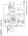
- FIG 1 there is shown a circuit diagram of a typical example of a hook monitor circuit, which is one of monitor circuits and which first operates in the subscriber circuit when a subscriber makes a telephone call.
- the shown hook monitor circuit is generally designated with Reference Numeral 1A, and connected to a pair of subscriber lines "Tip” and “Ring” which are interconnected within a telephone set when a handset is lifted (off hook).
- the shown hook monitor circuit includes a resistor R11 connected at its end to the subscriber line “Tip” and another resistor R12 connected at its end to the subscriber line “Ring", an amplifier A1 having an output connected to the other end of the resistor R11, an amplifier A2 having an output connected to the other end of the resistor R12, and a power feeding controlling circuit 11 for detecting a level on each of the subscriber line "Tip” and the subscriber line “Ring", so as to supplying a predetermined level of power supply voltage to the subscriber telephone set through the amplifiers A1 and A2, the resistors R11 and R12 and the subscriber lines "Tip” and “Ring”.
- the shown hook monitor circuit also includes an amplifier A3 for detecting and amplifying a voltage across the resistor R11, an amplifier A4 for detecting and amplifying a voltage across the resistor R12, an adder 12 for summing output voltages of the amplifiers A3 and A4, and a comparator 13A for comparing an output voltage of the adder 12 with a reference voltage Vr11 and for generating an active hook monitor signal HS when the output voltage of the adder 12 becomes higher than the reference voltage Vr11.
- the amplifiers A1 to A4 and the power feeding controlling circuit 11 operate with a power supply voltage Vbb of - 48V, which is the same level as that of a voltage supply for supplying an electric power to the telephone set.
- the comparator 13A operates with a power supply voltage Vcc of +5V, which is the same as an operating power supply voltage for signal processing and controlling circuits (called “internal circuits” hereinafter) within the telephone set. Accordingly, the power supply voltage Vcc is different from, the power supply voltage Vbb.
- hook monitor circuit 1A when the handset of the subscriber telephone set is hooked off or lifted off, the subscriber lines "Tip" and “Ring” are interconnected within the telephone set, so that there is formed a closed loop composed of the power feeding controlling circuit 11 ⁇ the amplifier A1 ⁇ the resistor R11 ⁇ the subscriber line “Tip” ⁇ the subscriber line “Ring” ⁇ the resistor R12 ⁇ the amplifier A2 ⁇ the power feeding controlling circuit 11, and a loop current flows through the closed loop thus formed.
- This loop current causes a voltage drop across each of the resistors R11 and R12, and the voltage drop is detected and amplified by each of the amplifiers A3 and A4.
- the two amplified voltage drops are summed by the adder 12, and then, supplied to the comparator 13A.
- the output voltage of the adder 12 is compared will, the reference voltage Vr11 predetermined by a voltage source E11.
- the comparator 13A generates an active hook monitor signal HS (high level) when the output voltage of the adder 12 becomes higher than the reference voltage Vr11 and an inactive hook monitor signal HS (low level) when the output voltage of the adder 12 becomes lower than the reference voltage Vr11. In the off-hook condition, since the voltage drop across the resistors R11 and R12 are large because of the loop current, the comparator 13A ordinarily generates the active hook monitor signal HS of the high level.
- Another object of the present invention is to provide a subscriber circuit having a monitor circuit capable of generating only a monitor signal of a normal monitor level.
- a subscriber circuit comprising a monitor circuit operating with a power supply voltage supplied to a subscriber instrument and monitoring an operation of the subscriber instrument for generating a monitor signal indicative of the result of monitor, a power supply voltage abnormality detecting circuit receiving the power supply voltage supplied to the subscriber instrument, for generating an active abnormality detection signal when the power supply voltage deviates from a predetermined voltage range, and means responding to the active abnormality detection signal for inhibiting the monitor circuit from outputting the monitor signal.
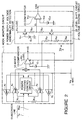
- FIG 2 there is shown a circuit diagram of one embodiment of the subscriber circuit in accordance with the present invention, including an power supply voltage abnormality detecting circuit.
- elements corresponding or similar to those shown in Figure 1 are given the same Reference Numerals, and explanation thereof will be omitted for simplification of description.
- This embodiment is different from the conventional subscriber circuit shown in Figure 1, in that it comprises a power supply voltage abnormality detecting circuit 2 generating an abnormality detection signal VAB, and a comparator 13 of a hook monitor circuit 1 has a control input receiving the active abnormality detection signal VAB, so that when the abnormality detection signal VAB is active, the comparator 13 is inhibited from outputting the monitor signal HS.
- the power supply voltage abnormality detecting circuit 2 includes a voltage dividing circuit 21, which is composed of three series-connected resistors R21, R22 and R23 connected between the ground level and the power supply voltage Vbb for the subscriber instruments, in the named order from the ground level. A divided voltage is picked up from a connection node between the resistors R21 and R22, and a voltage of Vbb/2 is obtained from a connection node between the resistors R22 and R23.
- the power supply voltage abnormality detecting circuit 2 also has a level shift circuit 22, which includes a PNP transistor Q21 having a base connected to the connection node between the resistors R21 and R22 and a collector connected to the power supply voltage Vbb, an NPN transistor having a base connected to a reference voltage source E21 so as to receive a reference voltage Vr21 and a collector connected to the power supply voltage Vcc for the internal circuits, and two series-connected resistors R24 and R25 connected between emitters of the transistors Q21 and Q22, so that a level-shifted voltage Vo is obtained from a connection node between the resistors R24 and R25.
- a level shift circuit 22 which includes a PNP transistor Q21 having a base connected to the connection node between the resistors R21 and R22 and a collector connected to the power supply voltage Vbb, an NPN transistor having a base connected to a reference voltage source E21 so as to receive a reference voltage Vr21 and a collector connected to the power supply voltage Vc
- connection node between the resistors R24 and R25 is connected to a first input of a comparator 23, which is driven with the power supply voltage Vcc, and which has its second input connected to a reference voltage source E22 so as to receive a reference voltage Vr22. Accordingly, the comparator 23 compares the level-shifted voltage Vo with the reference voltage Vr22 and generates an active or inactive abnormality detection signal VAB on the basis of the result of the comparison.
- the power supply voltage Vbb is voltage-divided and level-shifted into a level which can be easily handled in the comparator 23 that operates with the power supply voltage Vcc for the internal circuits.
- the voltage of Vbb/2 generated in the voltage dividing circuit 21 can be used in the power feeding controlling circuit 11.
- resistance values of the resistors R21, R22 and R23 are set to have a ratio of 1 : 1 : 2.
- Vo ⁇ Vr21 - Vbe(Q22) ⁇ R24/(R24+R25) + ⁇ Vbb/4+Vbe(Q21) ⁇ ⁇ R25/(R24+R25)
- Vbe(Q22) and Vbe(Q21) are a base-emitter voltage of the transistors Q21 and Q22, respectively, and are ordinarily on the order of 0.7V
- R24 and R25 are resistances of the resistors R24 and R25, respectively.
- the output voltage Vo of the level shift circuit 22 is compared with the reference voltage Vr22 in the comparator 23. For example, if the reference voltage Vr22 is set to be slightly lower than 2.4V, the comparator 23 outputs an inactive abnormality detection signal VAB in a normal condition and an active abnormality detection signal VAB in an abnormal condition, in the case of an example having the above mentioned numerical values.
- an output stage of the comparator 13 of the hook detection circuit 1 is composed of a CMOS structure including a transistor which is rendered off in response to the active abnormality detection signal VAB.
- the monitor signal HS is prevented from being outputted from the comparator 13, and an output of the comparator 13 is put in a high impedance condition, so that the output of the comparator 13 is isolated from a next stage circuit. Accordingly, although the monitor signal no longer assumes a normal monitor signal level because of the drop of the power supply voltage Vbb, no error monitor signal is outputted, so that there occurs no adverse influence by the error monitor signal.
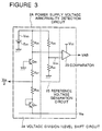
- FIG. 3 there is shown a circuit diagram of a second embodiment of the power supply voltage abnormality detecting circuit used in the subscriber circuit in accordance with the present invention.
- the second embodiment of the power supply voltage abnormality detecting circuit is generally designated with Reference Numeral 2A, and includes a voltage division and level shift circuit 24, which is composed of a resistor R26 connected at its one end to a reference voltage source E23 so as to receive a reference voltage Vr23, a base-grounded NPN transistor Q23 having its collector connected to the other end of the resistor R26, an NPN transistor Q24 having its emitter connected to the power supply voltage Vbb for the subscriber instruments and its base and its collector short-circuited, and two series-connected resistors R27 and R28 connected between an emitter of the transistor Q23 and the collector of the transistor Q24.
- a voltage division and level shift circuit 24 which is composed of a resistor R26 connected at its one end to a reference voltage source E23 so as to receive a reference voltage Vr23, a base-grounded NPN transistor Q23 having its collector connected to the other end of the resistor R26, an NPN transistor Q24 having its emitter connected to the power supply voltage Vb
- a voltage-divided and level-shifted voltage is obtained from a connection node between the resistor R26 and the collector of the transistors Q23, and a voltage of Vbb/2 is obtained from a connection node between the resistors R27 and R28.
- the shown power supply voltage abnormality detecting circuit 2A further includes a reference voltage generation circuit 25 composed of two series-connected resistors R29 and R30 connected between the reference voltage source E23 and the ground level, so that a reference voltage Vr24 is derived from a connection node between the resistors R29 and R30.
- the connection node between the resistor R26 and the collector of the transistors Q23 is connected to the first input of the comparator 23, and the connection node between the resistors R29 and R30 is connected to the second input of the comparator 23. Accordingly, the comparator 23 compares the voltage-divided and level-shifted voltage with the reference voltage Vr24 and generates an active or inactive abnormality detection signal VAB on the basis of the result of the comparison.
- the voltage division and level shift circuit 24 has both the function of the voltage dividing circuit 21 and the function of the level shift circuit 22 in the first embodiment; but can be constructed of a small number of circuit elements in comparison with the total number of circuit elements required for the circuits 21 and 22.
- the reference voltage Vr24 for the comparator is obtained from the voltage source E23 for the voltage division and level shift circuit 24, the number of necessary voltage sources can be reduced.
- a basic operation of the power supply voltage abnormality detecting circuit 2A is the same as that of the power supply voltage abnormality detecting circuit 2 in the first embodiment, and therefore, the power supply voltage abnormality detecting circuit 2A can exert a similar advantage. Accordingly, a further explanation will be omitted.
- the power supply voltage abnormality detecting circuits 2 and 2A generate the voltage of Vbb/2 which is required in the monitor circuit such as the hook monitor circuits 1 and 1A, it is unnecessary to provide a circuit (power supply voltage neutral point detection circuit) for generating the voltage of Vbb/2, and therefore, the number of necessary circuit elements can be correspondingly reduced.
Landscapes
- Engineering & Computer Science (AREA)
- Signal Processing (AREA)
- Monitoring And Testing Of Exchanges (AREA)
- Devices For Supply Of Signal Current (AREA)
- Interface Circuits In Exchanges (AREA)
Applications Claiming Priority (2)
| Application Number | Priority Date | Filing Date | Title |
|---|---|---|---|
| JP5142474A JP2639304B2 (ja) | 1993-06-15 | 1993-06-15 | 加入者回路 |
| JP142474/93 | 1993-06-15 |
Publications (2)
| Publication Number | Publication Date |
|---|---|
| EP0632632A2 true EP0632632A2 (de) | 1995-01-04 |
| EP0632632A3 EP0632632A3 (de) | 1996-10-16 |
Family
ID=15316164
Family Applications (1)
| Application Number | Title | Priority Date | Filing Date |
|---|---|---|---|
| EP94109210A Withdrawn EP0632632A3 (de) | 1993-06-15 | 1994-06-15 | Teilnehmerschaltung versehen mit einer Schaltung zur Überwachung eines Teilnehmergerätes. |
Country Status (3)
| Country | Link |
|---|---|
| US (1) | US5568547A (de) |
| EP (1) | EP0632632A3 (de) |
| JP (1) | JP2639304B2 (de) |
Cited By (1)
| Publication number | Priority date | Publication date | Assignee | Title |
|---|---|---|---|---|
| CN1080510C (zh) * | 1995-09-22 | 2002-03-06 | 日本电气株式会社 | 通过使用无须加恒流的平衡放大器控制挂机电压的电路 |
Families Citing this family (10)
| Publication number | Priority date | Publication date | Assignee | Title |
|---|---|---|---|---|
| KR0173403B1 (ko) * | 1996-04-25 | 1999-04-01 | 김광호 | 전화단말기의 통화로 자동복구 장치 및 그 방법 |
| SE507920C2 (sv) * | 1996-11-08 | 1998-07-27 | Ericsson Telefon Ab L M | Linjekrets |
| US6700975B1 (en) | 1996-11-08 | 2004-03-02 | Telefonaktiebolaget Lm Ericsson (Publ) | Subscriber line interface circuit |
| US6480510B1 (en) | 1998-07-28 | 2002-11-12 | Serconet Ltd. | Local area network of serial intelligent cells |
| US6956826B1 (en) | 1999-07-07 | 2005-10-18 | Serconet Ltd. | Local area network for distributing data communication, sensing and control signals |
| US6690677B1 (en) | 1999-07-20 | 2004-02-10 | Serconet Ltd. | Network for telephony and data communication |
| US6549616B1 (en) | 2000-03-20 | 2003-04-15 | Serconet Ltd. | Telephone outlet for implementing a local area network over telephone lines and a local area network using such outlets |
| US20020015489A1 (en) * | 2000-07-03 | 2002-02-07 | Shimon Ben-David | System and method for power feeding a line coupled to an exchange |
| IL154234A (en) | 2003-01-30 | 2010-12-30 | Mosaid Technologies Inc | Method and system for providing dc power on local telephone lines |
| IL159838A0 (en) | 2004-01-13 | 2004-06-20 | Yehuda Binder | Information device |
Family Cites Families (20)
| Publication number | Priority date | Publication date | Assignee | Title |
|---|---|---|---|---|
| NL7700719A (nl) * | 1977-01-25 | 1978-07-27 | Philips Nv | Storingsongevoelig lijnsupervisiecircuit. |
| US4164713A (en) * | 1977-01-28 | 1979-08-14 | Bell Telephone Laboratories, Incorporated | Dual mode telephone subscriber loop current detector |
| DE2850929C2 (de) * | 1978-11-24 | 1982-06-09 | Siemens AG, 1000 Berlin und 8000 München | Schaltungsanordnung zur Unterdrückung von Störspannungseinflüssen bei der Bewertung des Signalzustandes auf Übertragungsleitungen, insbesondere auf Teilnehmeranschlußleitungen in Fernsprechanlagen |
| US4455456A (en) * | 1982-04-26 | 1984-06-19 | International Telephone And Telegraph Corporation | Digital supervisory circuit for a telephone system |
| US4473719A (en) * | 1982-05-17 | 1984-09-25 | At&T Bell Laboratories | Switchhook status detector |
| US4446338A (en) * | 1982-07-12 | 1984-05-01 | Northern Telecom Limited | Telephone lines status sensor |
| JPS59115652A (ja) * | 1982-12-22 | 1984-07-04 | Hitachi Ltd | 加入者断線検出方式 |
| JPS60116264A (ja) * | 1983-11-29 | 1985-06-22 | Fujitsu Ltd | 交換機用異常監視装置 |
| CA1233583A (en) * | 1985-06-18 | 1988-03-01 | Francis Y. Hung | Protection arrangement for a telephone subscriber line interface circuit |
| JPS63100850A (ja) * | 1986-10-17 | 1988-05-02 | Tandei Electron Japan Kk | テレホンラインモニタ |
| JPH01117454A (ja) * | 1987-10-30 | 1989-05-10 | Canon Inc | 電話の着信報知方式 |
| US4937851A (en) * | 1988-07-20 | 1990-06-26 | Keptel, Inc. | Loop status verification system |
| JPH0272790A (ja) * | 1988-09-07 | 1990-03-13 | Fujitsu Ltd | ループ検出回路 |
| JPH02162995A (ja) * | 1988-12-16 | 1990-06-22 | Toshiba Corp | 電子式ボタン電話装置 |
| DE69120135T2 (de) * | 1990-04-04 | 1997-01-23 | Seiscor Tech Inc | Schnittstellenschaltung für Teilnehmerleitung, die regulierten Strom liefert |
| US5287404A (en) * | 1990-12-20 | 1994-02-15 | Northern Telecom Limited | Telephone subscriber line voltage change detection |
| JPH05268336A (ja) * | 1992-03-19 | 1993-10-15 | Fujitsu Ltd | リングトリップ回路 |
| US5337354A (en) * | 1992-07-30 | 1994-08-09 | Hubbell Incorporated | Tip-ring voltage correction circuit |
| JPH06244644A (ja) * | 1993-02-15 | 1994-09-02 | Pioneer Electron Corp | カーオーディオシステムにおけるミュート装置 |
| JP3034196U (ja) * | 1996-07-30 | 1997-02-14 | 有限会社小川鉄工所 | 農業用フィルムの穿孔器具 |
-
1993
- 1993-06-15 JP JP5142474A patent/JP2639304B2/ja not_active Expired - Fee Related
-
1994
- 1994-06-15 US US08/261,281 patent/US5568547A/en not_active Expired - Lifetime
- 1994-06-15 EP EP94109210A patent/EP0632632A3/de not_active Withdrawn
Cited By (1)
| Publication number | Priority date | Publication date | Assignee | Title |
|---|---|---|---|---|
| CN1080510C (zh) * | 1995-09-22 | 2002-03-06 | 日本电气株式会社 | 通过使用无须加恒流的平衡放大器控制挂机电压的电路 |
Also Published As
| Publication number | Publication date |
|---|---|
| JPH077545A (ja) | 1995-01-10 |
| JP2639304B2 (ja) | 1997-08-13 |
| US5568547A (en) | 1996-10-22 |
| EP0632632A3 (de) | 1996-10-16 |
Similar Documents
| Publication | Publication Date | Title |
|---|---|---|
| US4385336A (en) | Current supplying circuit with shorted-to-ground fault detecting function | |
| EP0632632A2 (de) | Teilnehmerschaltung versehen mit einer Schaltung zur Überwachung eines Teilnehmergerätes | |
| JPH06177660A (ja) | 増幅回路 | |
| EP0295683B1 (de) | Schutzschaltung für eine Batteriespeiseschaltung | |
| US5942945A (en) | Arrangement for protecting the output transistors in a power amplifier | |
| WO2006040935A1 (ja) | 演算増幅器 | |
| USRE33941E (en) | Power driver having short circuit protection | |
| JPH05145627A (ja) | リングトリツプ検出回路 | |
| EP3770613B1 (de) | Strommessschaltung und verfahren dafür | |
| US6949977B2 (en) | Circuit arrangement having a transimpedance amplifier connected to a current limiter circuit | |
| US6104168A (en) | Low leakage low dropout transistor charging circuit | |
| US7167557B2 (en) | Subscriber line interface circuit (SLIC) including a transient output current limit circuit and related method | |
| US5337354A (en) | Tip-ring voltage correction circuit | |
| JP2003198279A (ja) | モニタ回路および光受信器 | |
| KR100446390B1 (ko) | 액정표시소자의트랜지스터의동작체크회로 | |
| JPH0336859A (ja) | 電話機用電源回路 | |
| JP2002040060A (ja) | 監視回路 | |
| KR200143128Y1 (ko) | 과전류 보호 회로 | |
| JP2902334B2 (ja) | 火災警報受信機の受信回路 | |
| JPH03208108A (ja) | 定電流源回路 | |
| JP2005025697A (ja) | 2線式伝送回路 | |
| JP2021100199A (ja) | バッファ装置 | |
| JP2000151764A (ja) | 電話回線測定回路 | |
| JPH07234731A (ja) | 可変電流源回路 | |
| JPH04297121A (ja) | 比較回路 |
Legal Events
| Date | Code | Title | Description |
|---|---|---|---|
| PUAI | Public reference made under article 153(3) epc to a published international application that has entered the european phase |
Free format text: ORIGINAL CODE: 0009012 |
|
| AK | Designated contracting states |
Kind code of ref document: A2 Designated state(s): DE FR GB |
|
| PUAL | Search report despatched |
Free format text: ORIGINAL CODE: 0009013 |
|
| AK | Designated contracting states |
Kind code of ref document: A3 Designated state(s): DE FR GB |
|
| 17P | Request for examination filed |
Effective date: 19960904 |
|
| 17Q | First examination report despatched |
Effective date: 20010226 |
|
| GRAH | Despatch of communication of intention to grant a patent |
Free format text: ORIGINAL CODE: EPIDOS IGRA |
|
| STAA | Information on the status of an ep patent application or granted ep patent |
Free format text: STATUS: THE APPLICATION HAS BEEN WITHDRAWN |
|
| RAP1 | Party data changed (applicant data changed or rights of an application transferred) |
Owner name: NEC ELECTRONICS CORPORATION |
|
| 18W | Application withdrawn |
Effective date: 20030415 |