EP0632386A2 - System und Verfahren zur verbesserten Durchführung einer Pseudo-Zufallsprüfung von Systemen mit mehreren Bustreibern - Google Patents
System und Verfahren zur verbesserten Durchführung einer Pseudo-Zufallsprüfung von Systemen mit mehreren Bustreibern Download PDFInfo
- Publication number
- EP0632386A2 EP0632386A2 EP94304245A EP94304245A EP0632386A2 EP 0632386 A2 EP0632386 A2 EP 0632386A2 EP 94304245 A EP94304245 A EP 94304245A EP 94304245 A EP94304245 A EP 94304245A EP 0632386 A2 EP0632386 A2 EP 0632386A2
- Authority
- EP
- European Patent Office
- Prior art keywords
- scan
- test
- digital
- bus
- subsystems
- Prior art date
- Legal status (The legal status is an assumption and is not a legal conclusion. Google has not performed a legal analysis and makes no representation as to the accuracy of the status listed.)
- Withdrawn
Links
- 238000012360 testing method Methods 0.000 title claims abstract description 111
- 238000000034 method Methods 0.000 title claims abstract description 22
- 230000004044 response Effects 0.000 claims description 4
- 230000008878 coupling Effects 0.000 claims description 2
- 238000010168 coupling process Methods 0.000 claims description 2
- 238000005859 coupling reaction Methods 0.000 claims description 2
- 238000013459 approach Methods 0.000 description 7
- 238000010998 test method Methods 0.000 description 5
- 230000008569 process Effects 0.000 description 4
- 230000008901 benefit Effects 0.000 description 3
- 238000010586 diagram Methods 0.000 description 3
- 230000001360 synchronised effect Effects 0.000 description 3
- 238000004891 communication Methods 0.000 description 2
- 239000013598 vector Substances 0.000 description 2
- 230000015572 biosynthetic process Effects 0.000 description 1
- 238000010276 construction Methods 0.000 description 1
- 125000004122 cyclic group Chemical group 0.000 description 1
- 238000013461 design Methods 0.000 description 1
- 230000000694 effects Effects 0.000 description 1
- 230000006870 function Effects 0.000 description 1
- 230000010354 integration Effects 0.000 description 1
- 230000008520 organization Effects 0.000 description 1
- 238000012545 processing Methods 0.000 description 1
- 230000003134 recirculating effect Effects 0.000 description 1
- 238000012163 sequencing technique Methods 0.000 description 1
Images

Classifications
-
- G—PHYSICS
- G06—COMPUTING; CALCULATING OR COUNTING
- G06F—ELECTRIC DIGITAL DATA PROCESSING
- G06F11/00—Error detection; Error correction; Monitoring
- G06F11/22—Detection or location of defective computer hardware by testing during standby operation or during idle time, e.g. start-up testing
- G06F11/2205—Detection or location of defective computer hardware by testing during standby operation or during idle time, e.g. start-up testing using arrangements specific to the hardware being tested
- G06F11/2221—Detection or location of defective computer hardware by testing during standby operation or during idle time, e.g. start-up testing using arrangements specific to the hardware being tested to test input/output devices or peripheral units
-
- G—PHYSICS
- G01—MEASURING; TESTING
- G01R—MEASURING ELECTRIC VARIABLES; MEASURING MAGNETIC VARIABLES
- G01R31/00—Arrangements for testing electric properties; Arrangements for locating electric faults; Arrangements for electrical testing characterised by what is being tested not provided for elsewhere
- G01R31/28—Testing of electronic circuits, e.g. by signal tracer
- G01R31/317—Testing of digital circuits
- G01R31/3181—Functional testing
- G01R31/3183—Generation of test inputs, e.g. test vectors, patterns or sequences
- G01R31/318385—Random or pseudo-random test pattern
-
- G—PHYSICS
- G01—MEASURING; TESTING
- G01R—MEASURING ELECTRIC VARIABLES; MEASURING MAGNETIC VARIABLES
- G01R31/00—Arrangements for testing electric properties; Arrangements for locating electric faults; Arrangements for electrical testing characterised by what is being tested not provided for elsewhere
- G01R31/28—Testing of electronic circuits, e.g. by signal tracer
- G01R31/317—Testing of digital circuits
- G01R31/3181—Functional testing
- G01R31/3185—Reconfiguring for testing, e.g. LSSD, partitioning
- G01R31/318533—Reconfiguring for testing, e.g. LSSD, partitioning using scanning techniques, e.g. LSSD, Boundary Scan, JTAG
- G01R31/318555—Control logic
-
- G—PHYSICS
- G06—COMPUTING; CALCULATING OR COUNTING
- G06F—ELECTRIC DIGITAL DATA PROCESSING
- G06F11/00—Error detection; Error correction; Monitoring
- G06F11/22—Detection or location of defective computer hardware by testing during standby operation or during idle time, e.g. start-up testing
- G06F11/26—Functional testing
- G06F11/27—Built-in tests
Definitions
- the present invention is directed generally to testing digital apparatus such as is found in data processing systems.
- the invention relates more particularly to test techniques in which sequences of pseudo-random test patterns are shifted ("scanned") into and out of digital apparatus, producing resultant signatures from which can be determined whether or not the apparatus under test will function without fault.
- the invention provides a method, an apparatus implementing that method, for functionally scan testing a digital system of the type including a bus structure that is accessible by individual units on a mutually exclusive basis.
- LSI and VLSI produced a variety of techniques of for testing the very large amounts of digital circuitry that can found in integrated circuits (ICs) and combinations of ICs (e.g., as may be found on printed circuit or other types of boards and systems).
- One such technique involves application of a variety of known test signals to the IC or combination of ICs (hereinafter "digital system") and observing the output signals produced in response to determine if what was expected was produced by the digital system.
- One method of using these scan strings involves forming known test patterns ("vectors") that are put in place in the digital system by shifting (scanning") them into the system using the scan chains. The system is then allowed to run for a period of time (e.g., one or more clock periods), and the state of the system (i.e., the content of each memory stage) removed for observation, again using the scan chains.
- vectors known test patterns
- the system is then allowed to run for a period of time (e.g., one or more clock periods), and the state of the system (i.e., the content of each memory stage) removed for observation, again using the scan chains.
- the system is switched from the first or run mode to the scan mode for receiving pseudo-random bit patterns that are scanned into the scan strings to place the system in a pseudo-random state.
- the technique may include the step of returning the system momentarily to its run mode configuration, and permitting to operate for one clock cycle.
- the system is then returned to the scan mode, the digital state (i.e., the content of the scan string or strings) extracted (again by scanning), and that state then analyzed to determine the operability of the stages and interconnections of the system, and thereby the system itself.
- the steps of configuring the system to form the scan chains, scanning in the pseudo-random data, reinstating the normal configuration for an execution cycle, and returning the system to a scan configuration to remove (scan out) the resultant (pseudo-random) state is repeatedly performed with the extracted state compressed (such as through a cyclic redundancy) to form a "signature" that can be compared to a known, defect-free signature. If the signatures match, the test is considered to have been passed.
- This testing technique is usually referred to as "pseudo-random scan testing.”
- pseudo-random scan test methods include the test must be repeatable or "deterministic" in the sense that each time a digital system is tested, the results of that test will be the same if the system is without fault. Examples of such pseudo-random test methods and apparatus may be found in U.S Patent Nos. 4,718,065, 4,534,028, and 4,827,476.
- Pseudo-random scan testing can provide many benefits. It is a cost effective test method that can be performed without the need to form special test vectors in advance; it can be performed very fast to check or verify the operability of very large amounts of digital circuitry; and it can be performed using test circuitry less expensive and less complex than other test techniques. However, pseudo-random testing is not without certain problems.
- a flip side to the forgoing problem involves the situation of none of the subsystems are driving the shared bus, allowing it to float.
- the bus can assume a non-deterministic value, which one or more of the subsystems will attempt to read so that, again from test to test, different test results can be produced.
- One approach to solving this problem has been to include in the system a bus arbiter that receives requests for access to the bus. Using decoder circuitry, the arbiter issues a mutually exclusive bus enable signal to one and only one requester. This approach permits pseudo-random testing since the arbiter circuitry cannot permit more than one subsystem to drive the bus at any one moment in time. However, the approach tends to limit normal operating performance due to the extra time it takes to perform the arbitration. Thus, digital systems with such shared bus configurations have usually taken the approach of locking out the circuitry that drives the bus during pseudo-random testing, and the bus itself. This has resulted in the system not being completely tested - if tested at all.
- the present invention is directed to a digital system that includes a number of digital subsystems interconnected by a shared bus structure that is mutually exclusively accessible for communicating data between the digital subsystems.
- the present invention permits the bus access circuitry of each subsystem, and the bus itself, to be tested by pseudo-random scan testing methodology without restricting bus access to only one subsystem, and distributing that access during the test to all subsystems.
- each digital subsystem is provided with a counter that, during scan test periods, provides an enable signal to the bus access or driver circuitry of each subsystem.
- each counter is pre-loaded with a predetermined state so that, initially, and throughout the test period, one and only one digital subsystem will drive the shared data bus.
- Each scan sequence (each sequence being a scan in, an execution cycle, and a scan out of the pseudo-random test strings) will result in the counters being clocked once so that a new subsystem will be enable to drive the bus the next sequence.
- each of the counters is a ring counter in which a single bit is circulated to provide the enable signal.
- the enable signal to which the bus drive circuitry is responsive is developed from a pipelined organization that included a latch or register to hold the enable signal that controls the access or drive circuitry. This latch or register forms, during the scan test period, the last stage of the ring counter.
- the present invention provides a technique that enables inclusion in pseudo-random scan testing of a digital system the circuitry used by subsystems of that system for accessing a shared bus while still maintaining a test with deterministic results.
- pseudo-random scan testing may be performed without fear of damage to the shared bus.
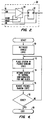
- a digital system 10 that comprises individual digital subsystems 12 (12a, 12b, ..., 12n).
- Subsystems 12 are interconnected by a shared bus 14 for communicating data and/or address signals thereon for inter-subsystem communication.
- the subsystems 12 could, for example, be one or more processor units, input/output (I/O) channel(s), memory system(s), and the like, with each of the subsystems capable of accessing the shared data bus 14 according to a predetermined protocol.
- That protocol is not important to the present invention, other than noting that the shared data bus 14 is accessible on a mutually exclusive basis; that is, only one of the subsystems 12 at any moment in time will be driving the shared data bus 14 with data, command, and/or address signals.
- the arbitration of access to the shared bus 14, in the event two or more of the subsystems 12 desire access to the bus at substantially the same time, is distributed in the sense that each subsystem arbitrates access to the bus on its own - according to a predetermined priority.
- a scan control logic unit 20 of generally conventional design that includes a 17 stage linear feedback shift register (LFSR - not shown) capable of developing 217-1 states before repeating.
- the scan control logic 20 will operate to develop the necessary test signals (scan, hold, bypass) used to perform scan testing of the subsystems 12 - including, of course, the pseudo-random patterns that are applied to the subsystems 12 via scan data in paths (sdi1, sdi2, ..., sdi n ) respectively coupling the scan control logic to the subsystems 12.
- the subsystems 12 will be constructed in accordance with conventional scan test techniques; that is, the elemental memory stages (i.e., the single bit storage elements (not shown) used for flip flops, latches, and the like) used in the subsystems 12 will be designed to be selectively placed in one of two configurations in response the to the scan test signals supplied by the scan control logic 20: normal mode, or scan mode, in which the elemental memory stage is interconnected with its brethren in the subsystem 12 to form a one long shift register (or a number of smaller shift registers) when in a scan test mode. While the configurations of such elemental memory stages are various and well known, it is believed that the present invention will be better appreciated and understood if the preferred construction of such elemental memory stages is considered.
- the memory stage 30 comprises a basic storage element 32 that receives, at its data (D) input, the output of a multiplexer 34.
- the output (Q) of the storage element 32 forms the output of the memory stage 30.
- the storage element 32 receives, at it clock (CK) input, a clock (CLK) signal that is instrumental in storing the data then applied to its data input (D) in conventional fashion.
- the multiplexer is constructed to receive data signals at its data (d) and scan data (sdi) inputs.
- the third input of the multiplexer 34 receives the output of the storage element 32.
- the selection between which of the inputs to the multiplexer 34 is communicated to the data input (D) of the storage element 32 is determined by the scan the signals applied to the scan and hold inputs, according to Table I, below. TABLE I SCAN HOLD DATA OUT 0 0 DATA IN (d) 1 0 SCAN DATA IN (sdi) 1 1 Q 0 1 Q
- the storage element 32 when neither of the signals applied to the scan and hold inputs are asserted the storage element 32 receives the signal received at the data input, d, of the stage 30. Conversely, when the signal applied to the scan input is asserted, the data (D) input of the storage element 32 will receive the whatever is applied to the scan data (sdi) input of the stage 30. Finally, if the signal applied to the hold input is asserted, irrespective of the state of whatever is applied to the scan input, the data of the stage 30 is recirculated by returning to the data (D) input of the storage element 32 its output Q each period of CLK. Thus, when the hold signal is asserted, the stage 20 holds the stored value until released from its held state.
- the clock (CLK) signal is the system clock used for synchronous operation of the elements of the subsystem.
- the scan control logic 20 when the scan control logic 20 asserts the scan signal to initiate the scan test mode, the elemental memory stages 30 of each sub-system are reconfigured from their normal functioning state to one that permits formation of the extended shift registers or scan strings that receive the initialization and pseudo-random data for the test. Pseudo-random data produced by the scan control logic is shifted into the scan strings of formed in each of the subsystems 12 via the scan data in lines sdi1, ..., sdi n , and scanned out via the scan data out lines sdo1, ..., sdo n .
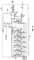
- the particular protocol to provide access to the shared bus 14 is not important to the present invention. What is important is to understand that, during normal operation, one and only one of the subsystems 12 is granted access, and allowed to drive, shared bus 14 for communicating data thereon to one or more of the other subsystems 12. Since, when the subsystems 12 are placed in pseudo-random states, this requirement for sharing the shared data bus 14 must be maintained, the present invention is provided, and illustrated in Fig. 3.
- Fig. 3 there is illustrated the bus driver circuit, designated generally with the reference numeral 40 for the subsystem 12a, together with the scan logic 42 that will control the bus driver circuit 40 of the subsystem 12a during scan tests.
- the remaining subsystems 12b, ..., 12n (Fig. 1) will include substantially identical circuitry so that the discussion of the enable circuit 40 and associated scan logic 42 of subsystem 12a should be taken to apply equally that circuitry of subsystems 12b, ..., 12n, unless noted otherwise.
- the scan logic 42 for the bus driver circuit 40 includes a bus enable register 50, multiplexer 52, a string of registers 54a, ..., 54f, and a multiplexer 62.
- the registers 54a, ..., 54f and bus enable register 50 form a seven-stage ring counter.
- the bus enable circuit 40 which preferably is a tri-state device (i.e., the output of which is capable of assuming one of the three states of a logic HIGH, a logic LOW, or a high impedance state), receives at its input 44 data from logic (not shown) of the subsystem 12a for communication on the shared bus 14. That received data will be communicated to the shared bus 14, via its output 46, when the signal applied to the enable input 48 is asserted.
- the signal for enabling the driver circuitry 40 is supplied by the bus enable register 50 which, in turn, receives (at its data (d) input) sys_enable from the multiplexer 52.
- the signal for enabling the bus driver circuit 40 is supplied by the output of stage 54f, and received by the bus enable register at its scan data in (sdi) input.
- Hold, scan, and bypass are the test signals asserted by the scan control logic 20 during scan mode of operation.
- the bypass test signal is also used to wall off non-scannable circuitry - not shown - during the scan process.
- the stages of the counter 54 will be placed in hold state when the scan control logic 20 asserts (1) the hold signal, or (2) both the bypass and scan signals.
- the clock (CK) inputs of stages 54a, ..., 54f and drive enable register receive the system clock (CLK) signal used by the subsystem 12a for synchronous operation.
- CLK system clock
- the CLK signal is used for both normal and scan test operation. It will be appreciated that the individual stages 54a, ..., 54f of the ring counter 54, as well as the bus enable register 50 are constructed as described above with reference to Fig. 2.
- each of the register stages 54a, 54b, 54c, 54d, and 54e are, as shown, coupled to the data (d) and scan data in (sdi) inputs of the next succeeding register stage 54b, ..., 54f, respectively, of the ring counter 54.
- the bus enable register 50 receives the output of the register stage 54f at its scan data input (sdi), and receives at its data (d) input, as indicated above, the output of the multiplexer 52.
- the multiplexer 52 is controlled by a bypass signal to select between a system enable (sys_enable), developed during normal (non-test) operation, and the output of the counter stage 54f.
- Asserting bypass in effect, configures the stages 54a, ..., 54f and bus enable register 50 to form the ring counter 54.
- De-asserting bypass removes the stages 54a, ..., 54f from the any operating capacity in the subsystem.
- Fig. 3 also diagrammatically illustrates the remainder of the subsystem 12a in a scan mode configuration, showing the elemental memory stages (exclusive of the bus enable register 50) that make up the subsystem 12a configured in the scan string 60.
- the input to the scan string 60 is supplied by multiplexer 62 which is controlled by the bypass test signal to select between scan data (when bypass is asserted) and the output of the bus enable register 50 (when bypass is not asserted, such as when in a normal mode of operation, or when scanning in the initialization data).
- the selection made by the multiplexer 62 input is coupled to the scan string 60, and the output of scan string 60 forms the scan data out (sdo1) for the subsystem 12a.
- the number of stages used for the ring counter 54 (including the bus enable register 50) will be at least equal to, or more than, the number of subsystems 12, i.e., the number of elements sharing the bus 14.
- the number of stages is preferably selected to remove any correlation between the sequencing of the counter and the states assumed by the linear feedback shift register, contained in the scan control logic 20, to ensure that the two (the counter 54 and linear feedback shift register) will not achieve some form of synchronization in order to make the scan test procedure as random-looking as possible.
- the states assumed should be prime to each other.
- the number of subsystems is preferably less than seven, a prime number.
- the linear feedback shift register (not shown) is designed with 17 stages and, therefore, is capable of assuming 217 (i.e., 131,072) states.
- Fig. 4 is a general diagram of the flow sequence used when conducting a scan test.
- the test begins at step 70 with the scan control logic 20 (Fig. 1) asserting the scan signal (the bypass signal is, for now, left de-asserted) to initially form the ring counter 54.
- the scan control logic 20 Fig. 1 asserting the scan signal (the bypass signal is, for now, left de-asserted) to initially form the ring counter 54.
- the scan signal will also form the scan strings 60 (Fig. 3) in each of the subsystems 12, but this is not important at this stage of the test - which is to initialize the ring counters 54.
- step 70 continues with the scan control logic 20 supplying predetermined bit patterns to the scan data inputs (sdi1, ..., sdi n ) that are scanned into the ring counters 54.
- the predetermined bit patterns are such that one of the ring counters 54 (e.g., that in subsystem 12a) will be preset so that its bus enable register 50 contains a 1, and the remaining stages contain a 0.
- the other ring counters 54 (e.g., of subsystems 12b, ..., 12n) will have bit patterns that leave the bus enable registers 50 with a 0, and a 1 in one of the remaining stages 54a, ..., 54f; that is, the predetermined bit pattern is such that one and only one bus enable register 50 of the subsystems 12 will be enabled at any one time.
- the enable logic is now initialized for the pseudo-random scan test to follow. During this initialization process, circuitry (not shown) between the bus enable register 50 and the input 48 of the bus driver circuit 40 will operate to hold the bus driver circuit 40 in its tri-state mode. At the conclusion of the initialization, the content bus driver enable register 50 will control the mode to the bus driver circuit 40.
- the predetermined bit pattern may contain more that one "1" so that one or more of the ring counters 54 are present with a pattern with two or more "1s".
- This feature also allows the test to adapt to different configurations of the system 10. For example, if certain of the subsystems 12 have been removed from the system 10, other of the subsystems may be allowed to take over the bus access cycles that would be normally be allocated, during testing, to the removed subsystem 12. However, it remains that the bus enable register 50 of one and only one subsystem 12 will hold a "1" of the ring counter 54 so that only one subsystem 12 drives the shared bus 14 at any one time.
- Step 70 is exited in favor of step 72 with the scan control logic raising the bypass signal, keeping the scan signal asserted.
- the combination of scan and bypass will assert hold' to freeze the ring counters 54.
- the assertion of the bypass signal operates the multiplexer 62 to select and apply the scan data input (sdi1) to the scan string 60, effectively removing the ring counter 54 (including the bus enable register 50) from the scan chain of their particular subsystem 12.
- the scan control logic 20 will remain in step 72, asserting the scan and bypass signals, and applying a pseudo-random patterns to the scan data inputs sdi1, ..., sdi n for the requisite number of system clocks (CLK) required place the scan string 60, and thereby the subsystems 12 in a pseudo-random state.
- CLK system clocks
- step 74 the scan control logic 20 drops (de-asserts) the scan and hold signals.
- the subsystems 12 are returned to their normal configurations and allowed to execute on cycle of the system clock (CLK) before being returned to the scan test configuration by the scan control logic 20 with the assertion of the scan and hold test signals.
- CLK system clock
- step 74 the hold and scan test signals are all de-asserted to allow the subsystems 12 to momentarily returned to their normal configurations to execute one cycle of the system clock, CLK.
- the hold' signal applied to the ring counters 54 is also de-asserted so that the ring counters 54 of the subsystems 12 are released from their frozen states. They are then also allowed to operate for the one clock cycle to move the content of each of the stages of the ring counter 54 (i.e. stages 54a, ..., 54f and bus enable register 50) to the next stage (via the data (d) inputs since the scan signal is not, at this time, asserted), with the content of the bus enable register 50 moving (recirculating) to the ring counter stage 54a.
- the predetermined bit patterns to which the ring counters were preset during the initialization step 70 are shifted so that the bus driver circuit 40 that was enabled to drive the shared bus 14 during step 72 is replaced with another bus driver circuit.
- the step 74 is exited with assertion of the scan and hold signals.
- the ring counters 54 are returned to a frozen condition and the subsystems 12 reconfigured to form scans strings.
- the pseudo-random states of the subsystems 12 i.e., scan strings 60
- the pseudo-random states of the subsystems 12 are removed in step 76 and communicated to the control logic 20 for analysis via the scan data outputs sdo1, ..., sdo n .
- step 78 Conventional pseudo-random scan testing involves repeating the sequence of steps 72 - 76 a set number of times (e.g. the number of states capable of being assumed by the 17-stage linear feedback shift register before repeating any one of those states), so that the scan control logic 20 will check, at step 78, to see if the desired number of sequences have been performed. If step 78 concludes that all desired sequences have not been completed, the process will return to the step 72. If, however, the requisite number of sequences have been performed, the process exits at step 80.
- the predetermined pattern placed in the ring counters 54 is rotated one position each sequence during step 74. At all other times of each test sequence the counters 54 (and bus enable registers 50) are held fixed. It will be apparent, therefore, that since during any one test sequence only one of the subsystems 12 is allowed to drive the shared bus 14, and that one changes from sequence to sequence, not only are deterministic test results ensured, but the shared bus 14 and associated drive circuits are included in the test.
Landscapes
- Engineering & Computer Science (AREA)
- General Engineering & Computer Science (AREA)
- Physics & Mathematics (AREA)
- General Physics & Mathematics (AREA)
- Theoretical Computer Science (AREA)
- Computer Hardware Design (AREA)
- Quality & Reliability (AREA)
- Test And Diagnosis Of Digital Computers (AREA)
- Tests Of Electronic Circuits (AREA)
- Bus Control (AREA)
Applications Claiming Priority (2)
| Application Number | Priority Date | Filing Date | Title |
|---|---|---|---|
| US83419 | 1993-06-28 | ||
| US08/083,419 US5951703A (en) | 1993-06-28 | 1993-06-28 | System and method for performing improved pseudo-random testing of systems having multi driver buses |
Publications (2)
| Publication Number | Publication Date |
|---|---|
| EP0632386A2 true EP0632386A2 (de) | 1995-01-04 |
| EP0632386A3 EP0632386A3 (de) | 1996-12-18 |
Family
ID=22178194
Family Applications (1)
| Application Number | Title | Priority Date | Filing Date |
|---|---|---|---|
| EP94304245A Withdrawn EP0632386A3 (de) | 1993-06-28 | 1994-06-13 | System und Verfahren zur verbesserten Durchführung einer Pseudo-Zufallsprüfung von Systemen mit mehreren Bustreibern. |
Country Status (7)
| Country | Link |
|---|---|
| US (1) | US5951703A (de) |
| EP (1) | EP0632386A3 (de) |
| JP (1) | JPH07168732A (de) |
| KR (1) | KR950001522A (de) |
| CN (1) | CN1099166A (de) |
| AU (1) | AU671371B2 (de) |
| CA (1) | CA2124991A1 (de) |
Cited By (1)
| Publication number | Priority date | Publication date | Assignee | Title |
|---|---|---|---|---|
| US8683307B2 (en) | 2011-05-27 | 2014-03-25 | International Business Machines Corporation | Checksum calculation, prediction and validation |
Families Citing this family (13)
| Publication number | Priority date | Publication date | Assignee | Title |
|---|---|---|---|---|
| EP1632780A2 (de) | 1995-12-27 | 2006-03-08 | Koken Co., Ltd. | Überwachungssteuerungsgerät |
| US5944845A (en) * | 1997-06-26 | 1999-08-31 | Micron Technology, Inc. | Circuit and method to prevent inadvertent test mode entry |
| US6851080B1 (en) * | 1999-02-05 | 2005-02-01 | 3Com Corporation | Automatic activation of ASIC test mode |
| US7225374B2 (en) * | 2003-12-04 | 2007-05-29 | International Business Machines Corporation | ABIST-assisted detection of scan chain defects |
| US7395469B2 (en) * | 2004-04-08 | 2008-07-01 | International Business Machines Corporation | Method for implementing deterministic based broken scan chain diagnostics |
| US7356436B2 (en) * | 2005-02-02 | 2008-04-08 | International Business Machines Corporation | Method, system, and storage medium for estimating and improving test case generation |
| US7395470B2 (en) * | 2005-06-09 | 2008-07-01 | International Business Machines Corporation | Method, apparatus, and computer program product for diagnosing a scan chain failure employing fuses coupled to the scan chain |
| US7930601B2 (en) * | 2008-02-22 | 2011-04-19 | International Business Machines Corporation | AC ABIST diagnostic method, apparatus and program product |
| JP5787829B2 (ja) * | 2012-06-01 | 2015-09-30 | 株式会社東芝 | マルチプロセッサ |
| JP6491507B2 (ja) * | 2015-03-20 | 2019-03-27 | ルネサスエレクトロニクス株式会社 | 半導体装置、電子装置および半導体装置の自己診断方法 |
| US10467211B2 (en) | 2017-11-15 | 2019-11-05 | International Business Machines Corporation | Representing and analyzing cloud computing data as pseudo systems |
| TWI640996B (zh) * | 2017-12-21 | 2018-11-11 | 新唐科技股份有限公司 | 記憶體電路及其測試方法 |
| US10778709B2 (en) | 2018-10-31 | 2020-09-15 | International Business Machines Corporation | Cloud-native extensibility provided to security analytics |
Citations (5)
| Publication number | Priority date | Publication date | Assignee | Title |
|---|---|---|---|---|
| JPS59188572A (ja) * | 1983-04-11 | 1984-10-25 | Seiko Epson Corp | 半導体試験回路 |
| US4860290A (en) * | 1987-06-02 | 1989-08-22 | Texas Instruments Incorporated | Logic circuit having individually testable logic modules |
| EP0417905A2 (de) * | 1989-08-09 | 1991-03-20 | Texas Instruments Incorporated | Architektur des Abtastpfads eines Systems |
| EP0578386A2 (de) * | 1992-06-17 | 1994-01-12 | Texas Instruments Incorporated | Hierarchisches Verbindungsverfahren, -gerät und -protokoll |
| US5331643A (en) * | 1991-09-04 | 1994-07-19 | International Business Machines Corporation | Self-testing logic with embedded arrays |
Family Cites Families (32)
| Publication number | Priority date | Publication date | Assignee | Title |
|---|---|---|---|---|
| US3783254A (en) * | 1972-10-16 | 1974-01-01 | Ibm | Level sensitive logic system |
| IT1047437B (it) * | 1975-10-08 | 1980-09-10 | Cselt Centro Studi Lab Telecom | Procedimento e dispositivo per il controllo in linea di memorie logiche sequenziali operanti a divisione di tempo |
| US4216539A (en) * | 1978-05-05 | 1980-08-05 | Zehntel, Inc. | In-circuit digital tester |
| US4326290A (en) * | 1979-10-16 | 1982-04-20 | Burroughs Corporation | Means and methods for monitoring the storage states of a memory and other storage devices in a digital data processor |
| DE3135368A1 (de) * | 1981-09-07 | 1983-03-31 | Siemens AG, 1000 Berlin und 8000 München | Verfahren und anordnung zur funktionspruefung einer programmierbare logikanordnung |
| US4513418A (en) * | 1982-11-08 | 1985-04-23 | International Business Machines Corporation | Simultaneous self-testing system |
| DE3379354D1 (en) * | 1983-05-25 | 1989-04-13 | Ibm Deutschland | Test and diagnostic device for a digital computer |
| US4575674A (en) * | 1983-07-01 | 1986-03-11 | Motorola, Inc. | Macrocell array having real time diagnostics |
| US4594711A (en) * | 1983-11-10 | 1986-06-10 | Texas Instruments Incorporated | Universal testing circuit and method |
| US4534028A (en) * | 1983-12-01 | 1985-08-06 | Siemens Corporate Research & Support, Inc. | Random testing using scan path technique |
| US4602210A (en) * | 1984-12-28 | 1986-07-22 | General Electric Company | Multiplexed-access scan testable integrated circuit |
| DE3580909D1 (de) * | 1985-01-04 | 1991-01-24 | Ibm Deutschland | Pruef- und diagnoseeinrichtung fuer digitalrechner. |
| US4801870A (en) * | 1985-06-24 | 1989-01-31 | International Business Machines Corporation | Weighted random pattern testing apparatus and method |
| NL8502476A (nl) * | 1985-09-11 | 1987-04-01 | Philips Nv | Werkwijze voor het testen van dragers met meerdere digitaal-werkende geintegreerde schakelingen, drager voorzien van zulke schakelingen, geintegreerde schakeling geschikt voor het aanbrengen op zo'n drager, en testinrichting voor het testen van zulke dragers. |
| US4701921A (en) * | 1985-10-23 | 1987-10-20 | Texas Instruments Incorporated | Modularized scan path for serially tested logic circuit |
| US5032783A (en) * | 1985-10-23 | 1991-07-16 | Texas Instruments Incorporated | Test circuit and scan tested logic device with isolated data lines during testing |
| FR2595474B1 (fr) * | 1986-03-04 | 1988-06-24 | Texas Instruments France | Dispositif de controle et de verification du fonctionnement de blocs internes a un circuit integre |
| US4718065A (en) * | 1986-03-31 | 1988-01-05 | Tandem Computers Incorporated | In-line scan control apparatus for data processor testing |
| JPH0821028B2 (ja) * | 1986-04-23 | 1996-03-04 | 株式会社日立製作所 | デ−タ処理装置 |
| US4827476A (en) * | 1987-04-16 | 1989-05-02 | Tandem Computers Incorporated | Scan test apparatus for digital systems having dynamic random access memory |
| US5173904A (en) * | 1987-06-02 | 1992-12-22 | Texas Instruments Incorporated | Logic circuits systems, and methods having individually testable logic modules |
| US4817093A (en) * | 1987-06-18 | 1989-03-28 | International Business Machines Corporation | Method of partitioning, testing and diagnosing a VLSI multichip package and associated structure |
| JP2673298B2 (ja) * | 1987-12-17 | 1997-11-05 | 三菱電機株式会社 | セルフテスト機能付半導体集積回路 |
| US5012180A (en) * | 1988-05-17 | 1991-04-30 | Zilog, Inc. | System for testing internal nodes |
| JP2827229B2 (ja) * | 1988-10-14 | 1998-11-25 | 日本電気株式会社 | 半導体集積回路 |
| JPH0758319B2 (ja) * | 1989-02-07 | 1995-06-21 | 株式会社東芝 | テスト容易化回路 |
| US4875003A (en) * | 1989-02-21 | 1989-10-17 | Silicon Connections Corporation | Non-contact I/O signal pad scan testing of VLSI circuits |
| GB9008544D0 (en) * | 1990-04-17 | 1990-06-13 | Smiths Industries Plc | Electrical assemblies |
| US5185745A (en) * | 1990-05-14 | 1993-02-09 | Prime Computer, Inc. | Scan path diagnostic method |
| US5210757A (en) * | 1990-10-05 | 1993-05-11 | Bull Hn Information Systems Inc. | Method and apparatus for performing health tests of units of a data processing system |
| US5293123A (en) * | 1990-10-19 | 1994-03-08 | Tandem Computers Incorporated | Pseudo-Random scan test apparatus |
| US5132635A (en) * | 1991-03-05 | 1992-07-21 | Ast Research, Inc. | Serial testing of removable circuit boards on a backplane bus |
-
1993
- 1993-06-28 US US08/083,419 patent/US5951703A/en not_active Expired - Fee Related
-
1994
- 1994-06-02 CA CA002124991A patent/CA2124991A1/en not_active Abandoned
- 1994-06-13 EP EP94304245A patent/EP0632386A3/de not_active Withdrawn
- 1994-06-27 JP JP6144503A patent/JPH07168732A/ja active Pending
- 1994-06-27 AU AU66006/94A patent/AU671371B2/en not_active Ceased
- 1994-06-27 KR KR1019940014781A patent/KR950001522A/ko not_active Application Discontinuation
- 1994-06-28 CN CN94107767A patent/CN1099166A/zh active Pending
Patent Citations (5)
| Publication number | Priority date | Publication date | Assignee | Title |
|---|---|---|---|---|
| JPS59188572A (ja) * | 1983-04-11 | 1984-10-25 | Seiko Epson Corp | 半導体試験回路 |
| US4860290A (en) * | 1987-06-02 | 1989-08-22 | Texas Instruments Incorporated | Logic circuit having individually testable logic modules |
| EP0417905A2 (de) * | 1989-08-09 | 1991-03-20 | Texas Instruments Incorporated | Architektur des Abtastpfads eines Systems |
| US5331643A (en) * | 1991-09-04 | 1994-07-19 | International Business Machines Corporation | Self-testing logic with embedded arrays |
| EP0578386A2 (de) * | 1992-06-17 | 1994-01-12 | Texas Instruments Incorporated | Hierarchisches Verbindungsverfahren, -gerät und -protokoll |
Non-Patent Citations (1)
| Title |
|---|
| PATENT ABSTRACTS OF JAPAN vol. 9, no. 50 (P-339) [1773] & JP-A-59 188572 (SUWA SEIKOSHA K.K.) * |
Cited By (3)
| Publication number | Priority date | Publication date | Assignee | Title |
|---|---|---|---|---|
| US8683307B2 (en) | 2011-05-27 | 2014-03-25 | International Business Machines Corporation | Checksum calculation, prediction and validation |
| US8806315B2 (en) | 2011-05-27 | 2014-08-12 | International Business Machines Corporation | Checksum calculation, prediction and validation |
| US9214957B2 (en) | 2011-05-27 | 2015-12-15 | International Business Machines Corporation | Checksum calculation, prediction and validation |
Also Published As
| Publication number | Publication date |
|---|---|
| AU6600694A (en) | 1995-01-05 |
| EP0632386A3 (de) | 1996-12-18 |
| AU671371B2 (en) | 1996-08-22 |
| JPH07168732A (ja) | 1995-07-04 |
| CN1099166A (zh) | 1995-02-22 |
| CA2124991A1 (en) | 1994-12-29 |
| US5951703A (en) | 1999-09-14 |
| KR950001522A (ko) | 1995-01-03 |
Similar Documents
| Publication | Publication Date | Title |
|---|---|---|
| US5173904A (en) | Logic circuits systems, and methods having individually testable logic modules | |
| US4860290A (en) | Logic circuit having individually testable logic modules | |
| JP2590294B2 (ja) | 回路ボードテストシステムとテストベクトル供給システム及び生成方法 | |
| KR100267096B1 (ko) | 디버그 및 제조 테스트 목적을 위한 적응적 스캔 체인 | |
| EP0287303B1 (de) | Abfrageprüfgerät für digitale Systeme mit dynamischem Direktzugriffspeicher | |
| US5680543A (en) | Method and apparatus for built-in self-test with multiple clock circuits | |
| US5084874A (en) | Enhanced test circuit | |
| US5774475A (en) | Testing scheme that re-uses original stimulus for testing circuitry embedded within a larger circuit | |
| US5951703A (en) | System and method for performing improved pseudo-random testing of systems having multi driver buses | |
| KR100241058B1 (ko) | Jtag를 사용한 sdram 다이나믹 셀프 리프레쉬 입구 및 출구용 구조 및 방법 | |
| JP3333036B2 (ja) | 試験装置、試験装置を備えたシステムおよび試験方法 | |
| US20030056165A1 (en) | IC test cell with memory output connected to input multiplexer | |
| US7430698B2 (en) | Method and system for an on-chip AC self-test controller | |
| JPH10123223A (ja) | 集積回路のテスト用クロック発生方法および回路 | |
| US5488613A (en) | Scan test circuits for use with multiple frequency circuits | |
| EP0469238B1 (de) | Schaltungen mit reduzierter Verzögerung für Schieberegisterabtastkette | |
| JPH10143390A (ja) | テスト機構を有する処理システム | |
| JPS6134174B2 (de) | ||
| US5673274A (en) | Test method for semiconductor device | |
| EP0699920B1 (de) | Integrierte Halbleiterschaltung mit prüfbaren Blöcken | |
| EP0310152A2 (de) | Prüfüberlagerungsschaltung | |
| US5450455A (en) | Method and apparatus for including the states of nonscannable parts in a scan chain | |
| JP2008520980A (ja) | 集積回路及びマルチtap集積回路を試験する方法 | |
| KR0163967B1 (ko) | 테스트 동안 바운더리-스캔 포트에 의해 복수의 시스템을 제어하기 위한 방법 및 장치 | |
| JP2002100738A (ja) | 半導体集積回路及びテスト容易化回路の自動挿入方法 |
Legal Events
| Date | Code | Title | Description |
|---|---|---|---|
| PUAI | Public reference made under article 153(3) epc to a published international application that has entered the european phase |
Free format text: ORIGINAL CODE: 0009012 |
|
| AK | Designated contracting states |
Kind code of ref document: A2 Designated state(s): DE FR GB IT SE |
|
| PUAL | Search report despatched |
Free format text: ORIGINAL CODE: 0009013 |
|
| AK | Designated contracting states |
Kind code of ref document: A3 Designated state(s): DE FR GB IT SE |
|
| 17P | Request for examination filed |
Effective date: 19970515 |
|
| STAA | Information on the status of an ep patent application or granted ep patent |
Free format text: STATUS: THE APPLICATION HAS BEEN WITHDRAWN |
|
| 18W | Application withdrawn |
Withdrawal date: 19990618 |