EP0629998A2 - Magnetoresistive film, method of its fabrication and magnetoresistive sensor - Google Patents
Magnetoresistive film, method of its fabrication and magnetoresistive sensor Download PDFInfo
- Publication number
- EP0629998A2 EP0629998A2 EP94108770A EP94108770A EP0629998A2 EP 0629998 A2 EP0629998 A2 EP 0629998A2 EP 94108770 A EP94108770 A EP 94108770A EP 94108770 A EP94108770 A EP 94108770A EP 0629998 A2 EP0629998 A2 EP 0629998A2
- Authority
- EP
- European Patent Office
- Prior art keywords
- layer
- ferromagnetic
- magnetoresistive film
- particles
- electrically conductive
- Prior art date
- Legal status (The legal status is an assumption and is not a legal conclusion. Google has not performed a legal analysis and makes no representation as to the accuracy of the status listed.)
- Withdrawn
Links
Images


Classifications
-
- G—PHYSICS
- G01—MEASURING; TESTING
- G01R—MEASURING ELECTRIC VARIABLES; MEASURING MAGNETIC VARIABLES
- G01R33/00—Arrangements or instruments for measuring magnetic variables
- G01R33/02—Measuring direction or magnitude of magnetic fields or magnetic flux
- G01R33/06—Measuring direction or magnitude of magnetic fields or magnetic flux using galvano-magnetic devices
- G01R33/09—Magnetoresistive devices
-
- B—PERFORMING OPERATIONS; TRANSPORTING
- B82—NANOTECHNOLOGY
- B82Y—SPECIFIC USES OR APPLICATIONS OF NANOSTRUCTURES; MEASUREMENT OR ANALYSIS OF NANOSTRUCTURES; MANUFACTURE OR TREATMENT OF NANOSTRUCTURES
- B82Y10/00—Nanotechnology for information processing, storage or transmission, e.g. quantum computing or single electron logic
-
- B—PERFORMING OPERATIONS; TRANSPORTING
- B82—NANOTECHNOLOGY
- B82Y—SPECIFIC USES OR APPLICATIONS OF NANOSTRUCTURES; MEASUREMENT OR ANALYSIS OF NANOSTRUCTURES; MANUFACTURE OR TREATMENT OF NANOSTRUCTURES
- B82Y25/00—Nanomagnetism, e.g. magnetoimpedance, anisotropic magnetoresistance, giant magnetoresistance or tunneling magnetoresistance
-
- G—PHYSICS
- G01—MEASURING; TESTING
- G01R—MEASURING ELECTRIC VARIABLES; MEASURING MAGNETIC VARIABLES
- G01R33/00—Arrangements or instruments for measuring magnetic variables
- G01R33/02—Measuring direction or magnitude of magnetic fields or magnetic flux
- G01R33/06—Measuring direction or magnitude of magnetic fields or magnetic flux using galvano-magnetic devices
- G01R33/09—Magnetoresistive devices
- G01R33/093—Magnetoresistive devices using multilayer structures, e.g. giant magnetoresistance sensors
-
- G—PHYSICS
- G11—INFORMATION STORAGE
- G11B—INFORMATION STORAGE BASED ON RELATIVE MOVEMENT BETWEEN RECORD CARRIER AND TRANSDUCER
- G11B5/00—Recording by magnetisation or demagnetisation of a record carrier; Reproducing by magnetic means; Record carriers therefor
- G11B5/127—Structure or manufacture of heads, e.g. inductive
- G11B5/33—Structure or manufacture of flux-sensitive heads, i.e. for reproduction only; Combination of such heads with means for recording or erasing only
- G11B5/39—Structure or manufacture of flux-sensitive heads, i.e. for reproduction only; Combination of such heads with means for recording or erasing only using magneto-resistive devices or effects
- G11B5/3903—Structure or manufacture of flux-sensitive heads, i.e. for reproduction only; Combination of such heads with means for recording or erasing only using magneto-resistive devices or effects using magnetic thin film layers or their effects, the films being part of integrated structures
-
- H—ELECTRICITY
- H01—ELECTRIC ELEMENTS
- H01F—MAGNETS; INDUCTANCES; TRANSFORMERS; SELECTION OF MATERIALS FOR THEIR MAGNETIC PROPERTIES
- H01F10/00—Thin magnetic films, e.g. of one-domain structure
- H01F10/007—Thin magnetic films, e.g. of one-domain structure ultrathin or granular films
-
- H—ELECTRICITY
- H01—ELECTRIC ELEMENTS
- H01F—MAGNETS; INDUCTANCES; TRANSFORMERS; SELECTION OF MATERIALS FOR THEIR MAGNETIC PROPERTIES
- H01F10/00—Thin magnetic films, e.g. of one-domain structure
- H01F10/32—Spin-exchange-coupled multilayers, e.g. nanostructured superlattices
- H01F10/3227—Exchange coupling via one or more magnetisable ultrathin or granular films
- H01F10/3231—Exchange coupling via one or more magnetisable ultrathin or granular films via a non-magnetic spacer
-
- H—ELECTRICITY
- H10—SEMICONDUCTOR DEVICES; ELECTRIC SOLID-STATE DEVICES NOT OTHERWISE PROVIDED FOR
- H10N—ELECTRIC SOLID-STATE DEVICES NOT OTHERWISE PROVIDED FOR
- H10N50/00—Galvanomagnetic devices
- H10N50/80—Constructional details
- H10N50/85—Materials of the active region
-
- G—PHYSICS
- G11—INFORMATION STORAGE
- G11B—INFORMATION STORAGE BASED ON RELATIVE MOVEMENT BETWEEN RECORD CARRIER AND TRANSDUCER
- G11B5/00—Recording by magnetisation or demagnetisation of a record carrier; Reproducing by magnetic means; Record carriers therefor
- G11B5/127—Structure or manufacture of heads, e.g. inductive
- G11B5/33—Structure or manufacture of flux-sensitive heads, i.e. for reproduction only; Combination of such heads with means for recording or erasing only
- G11B5/39—Structure or manufacture of flux-sensitive heads, i.e. for reproduction only; Combination of such heads with means for recording or erasing only using magneto-resistive devices or effects
- G11B2005/3996—Structure or manufacture of flux-sensitive heads, i.e. for reproduction only; Combination of such heads with means for recording or erasing only using magneto-resistive devices or effects large or giant magnetoresistive effects [GMR], e.g. as generated in spin-valve [SV] devices
Definitions
- the present invention relates generally to magnetic transducers for reading information signals recorded in a magnetic medium and, more particularly, to a magnetoresistive film, to a method of fabricating said film and to a magnetoresistive sensor employing said film.
- MR magnetoresistive
- An MR sensor detects magnetic field signals through the resistance changes of a read element fabricated of a magnetic material as a function of the strength and direction of magnetic flux being sensed by the read element.
- AMR anisotropic magnetoresistive
- cos2 cosine
- the easy axis of magnetisation in each of the magnetic layers is set perpendicular to the applied magnetic signal such that the current in the MR sensor element provides a magnetic field in the magnetic layers parallel to the easy axis thus eliminating or minimizing Barkhausen noise in the sensor.
- a second, different and more pronounced magnetoresistive effect has also been described in which the change in resistance of a layered magnetic sensor is attributed to the spin-dependent transmission of conduction electrons between ferromagnetic layers via a nonmagnetic layer separating the ferromagnetic layers and the accompanying spin-dependent scattering at the layer interfaces.
- This magnetoresistive effect is variously referred to as the "giant magnetoresistive" or “spin valve” effect.
- Such a magnetoresistive sensor fabricated of the appropriate materials provides improved sensitivity and greater change in resistance than observed in sensors utilizing the AMR effect.
- the in-plane resistance between a pair of ferromagnetic layers separated by a nonmagnetic layer varies as the cosine (cos) of the angle between the magnetization in the two layers.
- U.S. Patent No. 4,949,039 to Grunberg describes a layered magnetic structure which yields enhanced MR effects caused by antiparallel alignment of the magnetizations in the magnetic layers.
- Grunberg lists ferromagnetic transition metals and alloys, but does not indicate preferred materials from the list for superior MR signal amplitude.
- Grunberg further describes the use of antiferromagnetic-type exchange coupling to obtain the antiparallel alignment in which adjacent layers of ferromagnetic materials are separated by a thin interlayer of Cr or Y.
- the spin valve structures described in the above-cited U.S. patent and patent application require that the direction of magnetization in one of the two ferromagnetic layers be fixed or "pinned" in a selected orientation such that under non-signal conditions the direction of magnetization in the other ferromagnetic layer is oriented perpendicular to the pinned layer magnetization. Additionally, in both the AMR and spin valve structures, in order to minimize Barkhausen noise, it is necessary to provide a longitudinal bias field to maintain at least the sensing portion of the read element in a single magnetic domain state. Thus, a means for both fixing the direction of the magnetization and providing a longitudinal bias field is required.
- an additional layer of antiferromagnetic material can be formed in contact with the ferromagnetic layer to provide an exchange-coupled bias field.
- an adjacent magnetically hard layer can be utilized to provide hard bias for the ferromagnetic layer.
- Granular Giant Magnetoresistance was first observed in thin films of nickel (Ni) in a quartz matrix prepared by co-deposition. More recently granular GMR has been reported in co-deposited phase segregating thin films incorporating a metallic matrix, such as single layer alloy heterogeneous systems such as cobalt-copper (Co-Cu), cobalt-silver (Co-Ag) and nickel-iron-silver (NiFe-Ag).
- a metallic matrix such as single layer alloy heterogeneous systems such as cobalt-copper (Co-Cu), cobalt-silver (Co-Ag) and nickel-iron-silver (NiFe-Ag).
- Co-Cu cobalt-copper
- Co-Ag cobalt-silver
- NiFe-Ag nickel-iron-silver
- the Co alloys are of materials that are immiscible at low temperatures. Annealing the metastable alloy causes the formation of fine Co precipitates, i.e., "grains", in a Cu or Ag matrix wherein the MR effect appears to vary inversely with the diameter of the average particle diameter.
- a granular magnetoresistive film comprises a first layer of a discontinuous or granular ferromagnet, consisting of isolated particles of ferromagnetic material, such as Ni or Co, for example, formed on a heated insulating substrate.
- a nonmagnetic conductive matrix material such as Cu, for example, is subsequently deposited onto the cooled substrate to provide conduction between the ferromagnetic particles.
- This bilayer structure differs significantly from co-deposited phase segregating thin films as reported in the prior art.
- the separate deposition of the ferromagnetic material provides control of the size and shape of the isolated ferromagnetic regions in the film, resulting in a reduction of the magnetic field required to observe magnetoresistance and eliminates the need for mutual insolubility of the ferromagnetic and matrix materials.
- the granular magnetic film is formed by depositing a ferromagnetic film which is sufficiently thin and under conditions of sufficient surface mobility to provide a discontinuous thin film consisting of physically separated particles of ferromagnetic material on an insulating substrate.
- the ferromagnetic particles in the resulting film are not (or very poorly) electrically connected to one another or are non-percolating. Further, the ferromagnetic particles are not magnetically exchange-coupled to each other, and the magnetization of each particle is random in direction.
- the granular ferromagnetic thin film is then overcoated with a thin film of a non magnetic, i.e., nonferromagnetic, electrically conductive material under conditions sufficient to provide a continuous overlaying thin film.
- the resistivity of the composite film will be high when the net magnetization of the ferromagnetic film is zero due to the spin dependent electron scattering of the randomly oriented ferromagnetic particles. Spin dependent scattering will decrease and the resistivity will be lowered when an external magnetic field is applied as the local magnetic moments tend to orient in the direction of the applied magnetic field and hence are locally aligned.
- a preferred embodiment of the single layer granular magnetoresistive film according to the principles of the present invention comprises a thin layer of a ferromagnetic material, such as cobalt (Co), for example, deposited on a silicon oxide (SiO2) coated silicon (Si) substrate by vacuum (UHV) deposition techniques at an elevated temperature.
- a ferromagnetic material such as cobalt (Co)
- SiO2 silicon oxide coated silicon
- UHV vacuum
- a thin film of a nonmagnetic conductive material such as copper (Cu), for example, is deposited by UHV evaporation at room temperature. Since the deposition conditions for the ferromagnetic film are controlled to produce a discontinuous film, the resulting thin film structure provides ferromagnetic particles or islands embedded in a nonmagnetic conductive matrix.
- the structure can be subsequently annealed to promote further phase separation of the ferromagnetic layer to control particle size, shape and spacing. It is important to control the particle size and, to a lesser degree, the particle shape by careful processing (i.e., substrate temperature during deposition, deposition rate, anneal temperatures, for example) to obtain optimal magnetoresistive effect. It is desirable that the particle spacing within the conductive matrix be less than the mean free path of the carriers within the matrix material while insuring magnetic isolation between the particles. Additionally, it is desirable to have the ferromagnetic material be the largest possible volume fraction to avoid conduction without spin polarization. The coercivity of the ferromagnetic particles is also determined by particle size and shape, and other magnetic anisotropic characteristics of the material.
- Prior art MR sensors require substantially single domain behavior of the ferromagnetic MR element and suffer from Barkhausen noise when domain wall motion (rather than magnetization rotation) occurs thus requiring the use of magnetic bias fields to maintain the signal sensing portion of the MR sensor in a single magnetic domain state.
- the present invention provides a MR sensor in which the magnetoresistive sensing element constitutes a plurality of magnetic domains in which the individual magnetic moments rotate in response to an applied magnetic field signal. Since the response is the result of the rotation of the magnetic moments with limited domain wall motion, the need for a longitudinal bias field to minimize
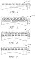
- Fig. 1 is a cross-sectional view illustrating a single layer granular magnetoresistive (MR) film fabricated according to the principles of the present invention.
- the granular MR film 10 comprises a discontinuous layer of ferromagnetic material, such as NiFe or Co, for example, deposited on a nonconductive layer 13 over a suitable substrate 11 to form a layer of ferromagnetic islands or particles 15.
- the layer of ferromagnetic material is deposited by evaporation or sputtering under ultra high vacuum conditions (UHV) and high substrate temperatures to provide sufficient mobility to allow the particles 15 of ferromagnetic material to form on the substrate overlayer 13.
- UHV ultra high vacuum conditions
- the substrate is then cooled and a continuous layer 17 of a nonmagnetic, electrically conductive material, such as Cu or Ag, for example, is deposited over the layer of ferromagnetic particles 15 by vacuum evaporation deposition thus forming a granular MR film wherein ferromagnetic particles 15 are embedded in a nonmagnetic, conductive matrix 17.
- a nonmagnetic, electrically conductive material such as Cu or Ag
- Suitable ferromagnetic materials are Fe, Co, Ni, NiFe and ferromagnetic alloys based on Fe, Co, Ni or NiFe.
- Suitable matrix materials are Au, Ag, Cu, ruthenium (Ru), palladium (Pd), rhodium (Rh) and conductive oxides such as cobalt oxide and nickel oxide, for example.
- the particles 15 will be all of generally the same shape and size.
- the size and shape of the particles 15 should be such as to form single magnetic domains within each particle and minimize shape anisotropy within the film.
- the observed MR effect in general, is inversely proportional to the ferromagnetic particle size. If the particle 15 dimensions are too large, the MR is reduced. Conversely, if the particle 15 dimensions are too small, large magnetic fields are required to produce an MR effect due to superparamagnetism.
- a suitable range for the ferromagnetic particles to provide a practical MR sensor is in the range of 10 ⁇ to 1000 ⁇ .
- the particles 15 should be separated by a distance less than the mean free path length for a conduction electron in the nonmagnetic matrix material, but having sufficient separation to minimize magnetic coupling. In an actual sample, there will be some variation in particle 15 size and shape and in separation distance for a given structure 10.
- an 80 Angstroms ( ⁇ ) (equivalent thickness) layer of Co is deposited on a 700 ⁇ thermal oxide layer 13 (SiO2) of a Si substrate 11 at 200 degrees C to form a discontinuous layer of ferromagnetic Co particles 15.
- the deposition is by electron beam evaporation in a chamber having a base pressure less than 10 ⁇ 10 mbar at deposition rates of approximately 0.2 ⁇ /second.
- Sputter deposition or other suitable vacuum thin film deposition techniques can also be used.
- the characteristic diameter of the particles 15 is approximately 300 ⁇ with an irregular oblate or pancake shape with a diameter approximately three times the thickness and an in-plane aspect ratio that is on the order of two.
- FIG. 2 is a cross-sectional view illustrating another preferred embodiment of the granular MR film 10 shown in Fig. 1.
- the granular MR film 10' comprises two discontinuous layers of ferromagnetic particles 15 and 16, each covered with a continuous layer 17 and 18, respectively, of a nonmagnetic conductive material to provide multiple layers of ferromagnetic particles 15, 16 in a nonmagnetic conductive matrix. Multiple particle conductive layers 16/18 will enhance the MR obtained significantly, but the bulk of the increases will be observed with the first two or three layers.
- Additional layers 15, 16 of ferromagnetic particles both increase the number of particles 15, 16 and increase the number of near neighbors for a particular particle thus increasing the number of scattering sites for the conduction electrons. Additionally the ratio of the volumes of ferromagnetic material to conductive material decreases thus decreasing the amount of current shunting by the conductive matrix material.
- the granular MR film 10' is fabricated in the same manner using UHV deposition techniques as described above with reference to Fig. 1.
- the nonmagnetic conductive material forming the underlaying matrix layer 17 must have a melting point that is greater than the temperature required for formation of the ferromagnetic particles 16 to minimize interdiffusion between the previously deposited matrix layers and the ferromagnetic material.
- Ru which has a relatively high melting temperature compared to Co is a suitable matrix material for this embodiment 10'.
- Fig. 3 illustrates a second embodiment of a multilayer granular MR film 10'' which includes an isolation layer 14 of a suitable material, such as SiO2, for example, deposited over the matrix layer 17 to provide a surface for deposition of the discontinuous ferromagnetic layer 16.
- the isolation layer 14 eases the deposition conditions required to form the subsequent layers of ferromagnetic particles 16, the improvement in MR magnitude is not as great as observed for the granular multilayer film 10' because the isolation layer 14 effectively prevents any interlayer scattering between the ferromagnetic particles 15 and 16.
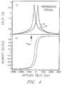
- Fig. 4 illustrates the magnetoresistance and magnetization measurements versus applied magnetic field for a granular MR structure 10 (as shown in Fig. 1) with a 50 ⁇ Co layer 15 deposited at 150 degrees C on a thermal oxide layer 13, overcoated with 80 ⁇ of Cu 17 and having a sheet resistance of 12 Ohms/square. All measures of the structures 10 were made at room temperature. Magnetoresistance was measured both perpendicular (curve 16) and parallel (curve 18) to the applied magnetic field. The difference between the two magnetoresistance measurement directions indicates residual anisotropic magnetoresistance (AMR) while the GMR is given as the average of the two measurements. A GMR of approximately 2.8 percent is observed.
- AMR anisotropic magnetoresistance
- FWHM full width at half maximum
- H sat saturation field
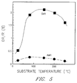
- Fig. 5 illustrates the GMR and AMR as a function of substrate temperature during deposition of the ferromagnetic layer 15 for a structure 10 having a 25 A layer 15 of NiFe on thermal oxide with an overcoat layer 17 of 40 ⁇ of Cu.
- the GMR peaks at a substrate temperature of approximately 150 degrees C.
- the decrease in GMR at higher deposition temperatures is due to the coarsening of the NiFe island structure at the higher temperatures.
- Table I provides results for structures 10 of different deposition thicknesses and clearly illustrates the effect of ferromagnetic island size.
- the larger GMR effect obtained for structures containing Co is expected from comparisons of Co and NiFe in continuous layer GMR structures.
- the lower saturation fields (as compared to the prior art cited above) obtained in the granular GMR structures of the present invention can be attributed to the reduced in-plane demagnetization of the pancake shape of the ferromagnetic particles 15.
- the fields required for magnetoresistance changes of NiFe structures are less than that for Co structures indicating that the crystalline anisotropy plays a role in the Co structures.
- the lower H c of the smaller particles may result from a more uniformly round shape, which is shown by Scanning Electron Microscope observations.
- a discontinuous layer of ferromagnetic particles 15 is formed on a nonconductive layer 13 over substrate 11 with an overlayer 17 of a nonmagnetic, conductive material formed over the layer of ferromagnetic particles 15.
- a continuous layer 19 of magnetic material is then formed over the overlayer 17 of conductive matrix material.
- Use of the magnetic overlayer 19 provides a substantial increase of the magnetoresistance observed for the structure 20.
- the magnetic overlayer 19 is likely to be multi-domain, in an actual sensing device, noise due to domain wall movement will be present.
- the magnetic overlayer 19 will be of a high coercivity material with its magnetic anisotropy initialized in a desired orientation to minimize Barkhausen noise.
- FIG. 7 a cross-section view of another preferred embodiment 30 of a single layer granular MR film fabricated according to the principles of the present invention is shown.
- a single layer film 25 of a ferromagnetic material and a nonmagnetic, conductive material is formed by co-sputtering from separate targets on a nonconductive layer 23 over a suitable substrate 21.
- the ferromagnetic and nonmagnetic conductive materials are co-deposited at room temperature and subsequently annealed at an elevated temperature to produce a heterogeneous film 25 of ferromagnetic particles 27 in a nonmagnetic conductive matrix 29.
- the ferromagnetic material and the nonmagnetic material are chosen such that the two materials are mutually immiscible in which phase separation of the materials will occur.
- the ferromagnetic and matrix materials can be miscible or partially miscible under equilibrium conditions processed in a controlled manner to limit interdiffusion.
- a 25 percent Co granular GMR film 25 is formed by co-sputtering Co and Cu from separate targets onto an oxidized Si substrate 21 and is subsequently annealed at temperatures in the range of 200 to 600 degrees C.
- Fig. 8 is a graph which illustrates the MR versus applied magnetic field obtained in the granular film having the above structure. While the higher anneal temperatures produce a lower MR value, both the magnetic fields required and the FWHM achieved are significantly lower. Since both Ni and Fe show very limited solubility in Ag and, conversely, Ag shows very little solubility in Ni or Fe at temperatures less than approximately 500 degrees C, granular MR films of NiFe/Ag are expected to show good results.
- NiFe systems are expected to exhibit lower values of MR.
- Other deposition or film-forming processes may also be used, such as, plating, ion deposition or pastes or other mechanical methods. Additionally, it is not required that the anneal process be performed subsequent to completion of the deposition process. Deposition may be done at elevated temperatures or on heated substrates to achieve the desired granular magnetic structures.
- the origin of the MR observed in the granular single layer structures 10, 20, 30 is believed to be primarily due to spin-dependent scattering of conduction electronics traversing the matrix between the magnetic regions or particles. While it is recognized that larger particles may comprise more than one or multiple magnetic moments, for analysis, it can be assumed that each of the particles behave as if it constituted a single magnetic moment or domain (as shown in Fig. 7). If the magnetic moments of the particles are randomly oriented, spin dependent scattering from particle to particle is increased resulting in a relatively high resistivity for the structure. On the other hand, if the magnetic moments of the particles are aligned in a parallel orientation, the resistance decreases to a relatively low value. While it is recognized that magnetostatic and exchange coupling exists between the particles in the matrix, a single particle model analysis which neglects interactions between particles is sufficient to show that the observed MR is strongly dependent on the particle size, shape and anisotropy.
- the MR sensor 40 comprises an MR sensing element 41, a bias layer 45 separated from the sensing element 41 by a nonmagnetic spacer layer 43 and is connected to a current source (not shown) by conductors 49 to provide a sensing current I to the MR sensor 41.
- the MR sensing element 41 is a granular magnetic structure as described above with reference to Figs. 1-3, 6 or 7 including a layer of ferromagnetic particles 15 in a metallic conductive matrix 17.
- the magnetic moments of the particles 15 may be partially oriented along an induced magnetic anisotropy axis, as shown by arrow 47.
- a magnetic anisotropy axis may be induced in the MR sensing element 41 by an annealing cycle in the presence of a magnetic field in the direction of the desired anisotropic axis, as is known in the art.
- the bias field provided by the bias layer 45 will further align the moments of the particles 15 in a desired direction to adjust the operating point of the MR sensor at a linear portion of its response characteristic.
- the MR sensor 40 is suspended above a data track 44 by a suspension apparatus (not shown) such that the magnetic field H at a data transition 46 will be applied in the plane of the sensing element 41.
- the magnetic moments rotate to align with the applied field H resulting in a decrease in the resistivity in the sensing element 41. Since rotation of the magnetization of the magnetic particles occurs with limited domain wall motion, a longitudinal bias field for the sensing element is not required.
Landscapes
- Engineering & Computer Science (AREA)
- Chemical & Material Sciences (AREA)
- Physics & Mathematics (AREA)
- Nanotechnology (AREA)
- Crystallography & Structural Chemistry (AREA)
- Power Engineering (AREA)
- General Physics & Mathematics (AREA)
- Condensed Matter Physics & Semiconductors (AREA)
- Mathematical Physics (AREA)
- Theoretical Computer Science (AREA)
- Manufacturing & Machinery (AREA)
- Hall/Mr Elements (AREA)
- Magnetic Heads (AREA)
- Measuring Magnetic Variables (AREA)
- Physical Vapour Deposition (AREA)
Applications Claiming Priority (2)
| Application Number | Priority Date | Filing Date | Title |
|---|---|---|---|
| US7965693A | 1993-06-18 | 1993-06-18 | |
| US79656 | 1998-03-26 |
Publications (2)
| Publication Number | Publication Date |
|---|---|
| EP0629998A2 true EP0629998A2 (en) | 1994-12-21 |
| EP0629998A3 EP0629998A3 (enExample) | 1995-01-04 |
Family
ID=22151959
Family Applications (1)
| Application Number | Title | Priority Date | Filing Date |
|---|---|---|---|
| EP94108770A Withdrawn EP0629998A2 (en) | 1993-06-18 | 1994-06-08 | Magnetoresistive film, method of its fabrication and magnetoresistive sensor |
Country Status (4)
| Country | Link |
|---|---|
| US (1) | US6016241A (enExample) |
| EP (1) | EP0629998A2 (enExample) |
| JP (1) | JP2793505B2 (enExample) |
| SG (1) | SG49605A1 (enExample) |
Cited By (5)
| Publication number | Priority date | Publication date | Assignee | Title |
|---|---|---|---|---|
| EP0797192A1 (en) * | 1996-03-19 | 1997-09-24 | Fujitsu Limited | Magnetic recording medium containing fine magnetic crystal grains and its manufacture |
| EP0911892A3 (en) * | 1997-10-23 | 1999-10-13 | Nec Corporation | Magneto-resistance effect device and method of manufacturing the same |
| US6214434B1 (en) * | 1997-09-02 | 2001-04-10 | Seagate Technology Llc | Isolated single-domain high-density magnetic recording media and method of manufacturing the media |
| RU2316078C1 (ru) * | 2006-10-13 | 2008-01-27 | Институт физики металлов УрО РАН | Магниторезистивный датчик |
| RU2386174C2 (ru) * | 2006-12-28 | 2010-04-10 | Валерий Андреевич Базыленко | Способ защиты от подделок и контроля подлинности ценных изделий |
Families Citing this family (24)
| Publication number | Priority date | Publication date | Assignee | Title |
|---|---|---|---|---|
| JP4496320B2 (ja) * | 1999-03-25 | 2010-07-07 | 独立行政法人産業技術総合研究所 | 磁気抵抗効果薄膜 |
| JP2000339635A (ja) * | 1999-05-31 | 2000-12-08 | Toshiba Corp | 磁気ヘッド及び磁気記録再生装置 |
| US6610602B2 (en) | 1999-06-29 | 2003-08-26 | The Research Foundation Of State University Of New York | Magnetic field sensor and method of manufacturing same using a self-organizing polymer mask |
| JP2001076331A (ja) * | 1999-09-02 | 2001-03-23 | Toshiba Corp | 磁気記録媒体及び磁気記録再生装置 |
| US6590751B1 (en) * | 1999-09-30 | 2003-07-08 | Headway Technologies, Inc. | Anisotropic magnetoresistive (MR) sensor element with enhanced magnetoresistive (MR) coefficient |
| US6727105B1 (en) * | 2000-02-28 | 2004-04-27 | Hewlett-Packard Development Company, L.P. | Method of fabricating an MRAM device including spin dependent tunneling junction memory cells |
| JP2002150512A (ja) * | 2000-11-08 | 2002-05-24 | Sony Corp | 磁気抵抗効果素子および磁気抵抗効果型磁気ヘッド |
| US6794862B2 (en) * | 2001-05-08 | 2004-09-21 | Ramot At Tel-Aviv University Ltd. | Magnetic thin film sensor based on the extraordinary hall effect |
| JP2003198004A (ja) * | 2001-12-27 | 2003-07-11 | Fujitsu Ltd | 磁気抵抗効果素子 |
| US7964924B2 (en) * | 2002-05-24 | 2011-06-21 | National Institute Of Advanced Industrial Science And Technology | Magnetoresistance effect device and magnetism sensor using the same |
| US7538987B2 (en) * | 2003-07-03 | 2009-05-26 | University Of Alabama | CPP spin-valve element |
| JP4786331B2 (ja) | 2005-12-21 | 2011-10-05 | 株式会社東芝 | 磁気抵抗効果素子の製造方法 |
| JP4514721B2 (ja) * | 2006-02-09 | 2010-07-28 | 株式会社東芝 | 磁気抵抗効果素子の製造方法、磁気抵抗効果素子、磁気抵抗効果ヘッド、磁気記録再生装置及び磁気記憶装置 |
| JP2007299880A (ja) * | 2006-04-28 | 2007-11-15 | Toshiba Corp | 磁気抵抗効果素子,および磁気抵抗効果素子の製造方法 |
| JP4550777B2 (ja) | 2006-07-07 | 2010-09-22 | 株式会社東芝 | 磁気抵抗効果素子の製造方法、磁気抵抗効果素子、磁気ヘッド、磁気記録再生装置及び磁気メモリ |
| JP5044157B2 (ja) * | 2006-07-11 | 2012-10-10 | 株式会社東芝 | 磁気抵抗効果素子,磁気ヘッド,および磁気再生装置 |
| JP2008085220A (ja) * | 2006-09-28 | 2008-04-10 | Toshiba Corp | 磁気抵抗効果素子、磁気ヘッド、および磁気再生装置 |
| JP4388093B2 (ja) | 2007-03-27 | 2009-12-24 | 株式会社東芝 | 磁気抵抗効果素子、磁気ヘッド、磁気記録再生装置 |
| JP5039007B2 (ja) | 2008-09-26 | 2012-10-03 | 株式会社東芝 | 磁気抵抗効果素子の製造方法、磁気抵抗効果素子、磁気ヘッドアセンブリ及び磁気記録再生装置 |
| JP5039006B2 (ja) | 2008-09-26 | 2012-10-03 | 株式会社東芝 | 磁気抵抗効果素子の製造方法、磁気抵抗効果素子、磁気ヘッドアセンブリ及び磁気記録再生装置 |
| JP2010080839A (ja) | 2008-09-29 | 2010-04-08 | Toshiba Corp | 磁気抵抗効果素子の製造方法、磁気抵抗効果素子、磁気ヘッドアセンブリおよび磁気記録再生装置 |
| KR101684915B1 (ko) * | 2010-07-26 | 2016-12-12 | 삼성전자주식회사 | 자기 기억 소자 |
| JP5850308B2 (ja) * | 2011-09-16 | 2016-02-03 | 株式会社豊田中央研究所 | ナノヘテロ構造軟磁性材料およびその製造方法 |
| JP5879854B2 (ja) * | 2011-09-16 | 2016-03-08 | 株式会社豊田中央研究所 | ナノヘテロ構造磁気抵抗素子、その製造方法、および磁気センサ |
Family Cites Families (12)
| Publication number | Priority date | Publication date | Assignee | Title |
|---|---|---|---|---|
| JPS58166510A (ja) * | 1982-03-29 | 1983-10-01 | Toshiba Corp | 磁気再生装置 |
| US4663242A (en) * | 1983-05-27 | 1987-05-05 | Olin Corporation | Method for producing a metal alloy strip |
| JPH07105006B2 (ja) * | 1985-11-05 | 1995-11-13 | ソニー株式会社 | 磁気抵抗効果型磁気ヘツド |
| DE3884756T2 (de) * | 1987-05-20 | 1994-05-05 | Matsushita Electric Ind Co Ltd | Verfahren zur herstellung eines dünnen films von basismetall und dessen verwendung. |
| DE3820475C1 (enExample) * | 1988-06-16 | 1989-12-21 | Kernforschungsanlage Juelich Gmbh, 5170 Juelich, De | |
| US4914538A (en) * | 1988-08-18 | 1990-04-03 | International Business Machines Corporation | Magnetoresistive read transducer |
| JPH03155102A (ja) * | 1989-11-13 | 1991-07-03 | Mitsubishi Electric Corp | 高導電性磁性材料 |
| US5043693A (en) * | 1990-08-13 | 1991-08-27 | The United States Of America As Represented By The Secretary Of The Navy | Heterogeneous magnetoresistive layer |
| US5206590A (en) * | 1990-12-11 | 1993-04-27 | International Business Machines Corporation | Magnetoresistive sensor based on the spin valve effect |
| US5159513A (en) * | 1991-02-08 | 1992-10-27 | International Business Machines Corporation | Magnetoresistive sensor based on the spin valve effect |
| US5268043A (en) * | 1991-08-02 | 1993-12-07 | Olin Corporation | Magnetic sensor wire |
| JPH07508133A (ja) * | 1992-06-16 | 1995-09-07 | ザ リージェンツ オブ ザ ユニバーシティ オブ カリフォルニア | 巨大な磁気抵抗性の単一膜合金 |
-
1994
- 1994-06-08 SG SG1996000761A patent/SG49605A1/en unknown
- 1994-06-08 EP EP94108770A patent/EP0629998A2/en not_active Withdrawn
- 1994-06-16 JP JP6134650A patent/JP2793505B2/ja not_active Expired - Fee Related
-
1995
- 1995-05-22 US US08/445,479 patent/US6016241A/en not_active Expired - Fee Related
Cited By (7)
| Publication number | Priority date | Publication date | Assignee | Title |
|---|---|---|---|---|
| EP0797192A1 (en) * | 1996-03-19 | 1997-09-24 | Fujitsu Limited | Magnetic recording medium containing fine magnetic crystal grains and its manufacture |
| US6171676B1 (en) | 1996-03-19 | 2001-01-09 | Fujitsu Limited | Magnetic recording medium containing fine magnetic crystal grains and its manufacture |
| US6214434B1 (en) * | 1997-09-02 | 2001-04-10 | Seagate Technology Llc | Isolated single-domain high-density magnetic recording media and method of manufacturing the media |
| EP0911892A3 (en) * | 1997-10-23 | 1999-10-13 | Nec Corporation | Magneto-resistance effect device and method of manufacturing the same |
| US6183890B1 (en) | 1997-10-23 | 2001-02-06 | Nec Corporation | Magneto-resistance effect device and method of manufacturing the same |
| RU2316078C1 (ru) * | 2006-10-13 | 2008-01-27 | Институт физики металлов УрО РАН | Магниторезистивный датчик |
| RU2386174C2 (ru) * | 2006-12-28 | 2010-04-10 | Валерий Андреевич Базыленко | Способ защиты от подделок и контроля подлинности ценных изделий |
Also Published As
| Publication number | Publication date |
|---|---|
| JPH0758375A (ja) | 1995-03-03 |
| EP0629998A3 (enExample) | 1995-01-04 |
| US6016241A (en) | 2000-01-18 |
| JP2793505B2 (ja) | 1998-09-03 |
| SG49605A1 (en) | 1998-06-15 |
Similar Documents
| Publication | Publication Date | Title |
|---|---|---|
| US6016241A (en) | Magnetoresistive sensor utilizing a granular magnetoresistive layer | |
| US5476680A (en) | Method for manufacturing granular multilayer mangetoresistive sensor | |
| US6292336B1 (en) | Giant magnetoresistive (GMR) sensor element with enhanced magnetoresistive (MR) coefficient | |
| EP0660127B1 (en) | Multilayer magnetoresistive sensor | |
| EP0598581B1 (en) | Magnetoresistive sensor | |
| EP0701142B1 (en) | Magnetoresistance effect film and production process thereof | |
| KR100261385B1 (ko) | 반평행 구속층과 개선된 바이어스층을 갖는 스핀 밸브 자기저항 센서와 그 센서를 이용한 자기 기록 시스템 | |
| CN1180400C (zh) | 磁盘记录系统和双磁电阻读传感器 | |
| US6340520B1 (en) | Giant magnetoresistive material film, method of producing the same magnetic head using the same | |
| US6295186B1 (en) | Spin-valve magnetoresistive Sensor including a first antiferromagnetic layer for increasing a coercive force and a second antiferromagnetic layer for imposing a longitudinal bias | |
| US5958611A (en) | Magnetic multilayered film, magnetoresistance effect element and magnetoresistance device | |
| US6914761B2 (en) | Magnetoresistive sensor with magnetic flux paths surrounding non-magnetic regions of ferromagnetic material layer | |
| US5764445A (en) | Exchange biased magnetoresistive transducer | |
| EP1400957A2 (en) | Spin-valve head containing partial current-screening-layer, production method of said head, and current-screening method | |
| JPH0821166B2 (ja) | 磁気抵抗センサ | |
| US7029771B2 (en) | Magnetic sensor having free layer additionally provided with magnetic anisotropy by shape anisotropy | |
| EP0672303A1 (en) | Magneto-resistance device, and magnetic head employing such a device | |
| JPH06220609A (ja) | 磁気抵抗効果膜及びその製造方法並びにそれを用いた磁気抵抗効果素子、磁気抵抗効果型磁気ヘッド | |
| JP3276264B2 (ja) | 磁気抵抗効果多層膜およびその製造方法 | |
| Parker et al. | Overview of progress in giant magnetoresistive sensors based on NiFe/Ag multilayers | |
| KR19980032686A (ko) | 자기저항 효과 막 및 그의 제조 방법 | |
| JPH0923031A (ja) | 磁気抵抗効果多層膜 | |
| JPH0992904A (ja) | 巨大磁気抵抗効果材料膜およびその製造方法とそれを用いた磁気ヘッド | |
| US6001430A (en) | Magnetoresistance effect film and production process thereof | |
| JPH08316033A (ja) | 磁性積層体 |
Legal Events
| Date | Code | Title | Description |
|---|---|---|---|
| PUAI | Public reference made under article 153(3) epc to a published international application that has entered the european phase |
Free format text: ORIGINAL CODE: 0009012 |
|
| PUAL | Search report despatched |
Free format text: ORIGINAL CODE: 0009013 |
|
| AK | Designated contracting states |
Kind code of ref document: A2 Designated state(s): DE FR GB |
|
| AK | Designated contracting states |
Kind code of ref document: A3 Designated state(s): DE FR GB |
|
| 17P | Request for examination filed |
Effective date: 19950425 |
|
| 17Q | First examination report despatched |
Effective date: 19970828 |
|
| STAA | Information on the status of an ep patent application or granted ep patent |
Free format text: STATUS: THE APPLICATION IS DEEMED TO BE WITHDRAWN |
|
| 18D | Application deemed to be withdrawn |
Effective date: 19980818 |