EP0629007A1 - Piezoelektrische Anordnung - Google Patents
Piezoelektrische Anordnung Download PDFInfo
- Publication number
- EP0629007A1 EP0629007A1 EP94304112A EP94304112A EP0629007A1 EP 0629007 A1 EP0629007 A1 EP 0629007A1 EP 94304112 A EP94304112 A EP 94304112A EP 94304112 A EP94304112 A EP 94304112A EP 0629007 A1 EP0629007 A1 EP 0629007A1
- Authority
- EP
- European Patent Office
- Prior art keywords
- layer
- piezoelectric
- substrate
- cavity
- piezoelectric device
- Prior art date
- Legal status (The legal status is an assumption and is not a legal conclusion. Google has not performed a legal analysis and makes no representation as to the accuracy of the status listed.)
- Granted
Links
- 239000000758 substrate Substances 0.000 claims abstract description 168
- 238000006073 displacement reaction Methods 0.000 claims abstract description 43
- 239000000919 ceramic Substances 0.000 claims abstract description 39
- 230000002093 peripheral effect Effects 0.000 claims abstract description 26
- 230000008859 change Effects 0.000 claims abstract description 10
- 239000000463 material Substances 0.000 claims description 53
- 239000000203 mixture Substances 0.000 claims description 19
- 239000013078 crystal Substances 0.000 claims description 8
- NKZSPGSOXYXWQA-UHFFFAOYSA-N dioxido(oxo)titanium;lead(2+) Chemical compound [Pb+2].[O-][Ti]([O-])=O NKZSPGSOXYXWQA-UHFFFAOYSA-N 0.000 claims description 8
- ZBSCCQXBYNSKPV-UHFFFAOYSA-N oxolead;oxomagnesium;2,4,5-trioxa-1$l^{5},3$l^{5}-diniobabicyclo[1.1.1]pentane 1,3-dioxide Chemical compound [Mg]=O.[Pb]=O.[Pb]=O.[Pb]=O.O1[Nb]2(=O)O[Nb]1(=O)O2 ZBSCCQXBYNSKPV-UHFFFAOYSA-N 0.000 claims description 8
- HFGPZNIAWCZYJU-UHFFFAOYSA-N lead zirconate titanate Chemical compound [O-2].[O-2].[O-2].[O-2].[O-2].[Ti+4].[Zr+4].[Pb+2] HFGPZNIAWCZYJU-UHFFFAOYSA-N 0.000 claims description 7
- RVTZCBVAJQQJTK-UHFFFAOYSA-N oxygen(2-);zirconium(4+) Chemical compound [O-2].[O-2].[Zr+4] RVTZCBVAJQQJTK-UHFFFAOYSA-N 0.000 claims description 6
- 229910001928 zirconium oxide Inorganic materials 0.000 claims description 6
- SIWVEOZUMHYXCS-UHFFFAOYSA-N oxo(oxoyttriooxy)yttrium Chemical compound O=[Y]O[Y]=O SIWVEOZUMHYXCS-UHFFFAOYSA-N 0.000 claims description 5
- BRPQOXSCLDDYGP-UHFFFAOYSA-N calcium oxide Chemical compound [O-2].[Ca+2] BRPQOXSCLDDYGP-UHFFFAOYSA-N 0.000 claims description 3
- 239000000292 calcium oxide Substances 0.000 claims description 3
- ODINCKMPIJJUCX-UHFFFAOYSA-N calcium oxide Inorganic materials [Ca]=O ODINCKMPIJJUCX-UHFFFAOYSA-N 0.000 claims description 3
- 229910000420 cerium oxide Inorganic materials 0.000 claims description 3
- HEPLMSKRHVKCAQ-UHFFFAOYSA-N lead nickel Chemical compound [Ni].[Pb] HEPLMSKRHVKCAQ-UHFFFAOYSA-N 0.000 claims description 3
- 239000000395 magnesium oxide Substances 0.000 claims description 3
- CPLXHLVBOLITMK-UHFFFAOYSA-N magnesium oxide Inorganic materials [Mg]=O CPLXHLVBOLITMK-UHFFFAOYSA-N 0.000 claims description 3
- AXZKOIWUVFPNLO-UHFFFAOYSA-N magnesium;oxygen(2-) Chemical compound [O-2].[Mg+2] AXZKOIWUVFPNLO-UHFFFAOYSA-N 0.000 claims description 3
- BMMGVYCKOGBVEV-UHFFFAOYSA-N oxo(oxoceriooxy)cerium Chemical compound [Ce]=O.O=[Ce]=O BMMGVYCKOGBVEV-UHFFFAOYSA-N 0.000 claims description 3
- 238000000034 method Methods 0.000 description 30
- 230000015572 biosynthetic process Effects 0.000 description 22
- 239000010408 film Substances 0.000 description 22
- 230000008569 process Effects 0.000 description 22
- 238000010304 firing Methods 0.000 description 13
- 230000003993 interaction Effects 0.000 description 12
- 230000000052 comparative effect Effects 0.000 description 11
- 238000010438 heat treatment Methods 0.000 description 11
- 238000004519 manufacturing process Methods 0.000 description 11
- 230000035882 stress Effects 0.000 description 10
- BASFCYQUMIYNBI-UHFFFAOYSA-N platinum Chemical compound [Pt] BASFCYQUMIYNBI-UHFFFAOYSA-N 0.000 description 8
- 238000005245 sintering Methods 0.000 description 8
- 229910010293 ceramic material Inorganic materials 0.000 description 6
- 230000006870 function Effects 0.000 description 5
- 238000007641 inkjet printing Methods 0.000 description 5
- 239000007772 electrode material Substances 0.000 description 4
- 238000002474 experimental method Methods 0.000 description 4
- 229910052451 lead zirconate titanate Inorganic materials 0.000 description 4
- 238000003754 machining Methods 0.000 description 4
- 229910052697 platinum Inorganic materials 0.000 description 4
- KDLHZDBZIXYQEI-UHFFFAOYSA-N Palladium Chemical compound [Pd] KDLHZDBZIXYQEI-UHFFFAOYSA-N 0.000 description 3
- 239000000654 additive Substances 0.000 description 3
- 239000000956 alloy Substances 0.000 description 3
- 229910045601 alloy Inorganic materials 0.000 description 3
- 239000011248 coating agent Substances 0.000 description 3
- 238000000576 coating method Methods 0.000 description 3
- 239000004020 conductor Substances 0.000 description 3
- 229910052751 metal Inorganic materials 0.000 description 3
- 239000002184 metal Substances 0.000 description 3
- 238000007639 printing Methods 0.000 description 3
- 238000007650 screen-printing Methods 0.000 description 3
- 230000003746 surface roughness Effects 0.000 description 3
- XEEYBQQBJWHFJM-UHFFFAOYSA-N Iron Chemical compound [Fe] XEEYBQQBJWHFJM-UHFFFAOYSA-N 0.000 description 2
- PXHVJJICTQNCMI-UHFFFAOYSA-N Nickel Chemical compound [Ni] PXHVJJICTQNCMI-UHFFFAOYSA-N 0.000 description 2
- VYPSYNLAJGMNEJ-UHFFFAOYSA-N Silicium dioxide Chemical compound O=[Si]=O VYPSYNLAJGMNEJ-UHFFFAOYSA-N 0.000 description 2
- GWEVSGVZZGPLCZ-UHFFFAOYSA-N Titan oxide Chemical compound O=[Ti]=O GWEVSGVZZGPLCZ-UHFFFAOYSA-N 0.000 description 2
- MCMNRKCIXSYSNV-UHFFFAOYSA-N Zirconium dioxide Chemical compound O=[Zr]=O MCMNRKCIXSYSNV-UHFFFAOYSA-N 0.000 description 2
- 229910052787 antimony Inorganic materials 0.000 description 2
- 238000005452 bending Methods 0.000 description 2
- 239000011195 cermet Substances 0.000 description 2
- 238000006243 chemical reaction Methods 0.000 description 2
- 238000005229 chemical vapour deposition Methods 0.000 description 2
- 238000004891 communication Methods 0.000 description 2
- 150000001875 compounds Chemical class 0.000 description 2
- 238000007598 dipping method Methods 0.000 description 2
- 230000000694 effects Effects 0.000 description 2
- 238000009413 insulation Methods 0.000 description 2
- 230000010354 integration Effects 0.000 description 2
- 238000005259 measurement Methods 0.000 description 2
- 229910052763 palladium Inorganic materials 0.000 description 2
- 239000000843 powder Substances 0.000 description 2
- 238000004080 punching Methods 0.000 description 2
- 229920005989 resin Polymers 0.000 description 2
- 239000011347 resin Substances 0.000 description 2
- 230000004044 response Effects 0.000 description 2
- 229910052814 silicon oxide Inorganic materials 0.000 description 2
- 238000005507 spraying Methods 0.000 description 2
- 239000000126 substance Substances 0.000 description 2
- 230000001629 suppression Effects 0.000 description 2
- OYPRJOBELJOOCE-UHFFFAOYSA-N Calcium Chemical compound [Ca] OYPRJOBELJOOCE-UHFFFAOYSA-N 0.000 description 1
- 229910052684 Cerium Inorganic materials 0.000 description 1
- VYZAMTAEIAYCRO-UHFFFAOYSA-N Chromium Chemical compound [Cr] VYZAMTAEIAYCRO-UHFFFAOYSA-N 0.000 description 1
- WHXSMMKQMYFTQS-UHFFFAOYSA-N Lithium Chemical compound [Li] WHXSMMKQMYFTQS-UHFFFAOYSA-N 0.000 description 1
- PWHULOQIROXLJO-UHFFFAOYSA-N Manganese Chemical compound [Mn] PWHULOQIROXLJO-UHFFFAOYSA-N 0.000 description 1
- HCHKCACWOHOZIP-UHFFFAOYSA-N Zinc Chemical compound [Zn] HCHKCACWOHOZIP-UHFFFAOYSA-N 0.000 description 1
- IHWJXGQYRBHUIF-UHFFFAOYSA-N [Ag].[Pt] Chemical compound [Ag].[Pt] IHWJXGQYRBHUIF-UHFFFAOYSA-N 0.000 description 1
- 230000000996 additive effect Effects 0.000 description 1
- PNEYBMLMFCGWSK-UHFFFAOYSA-N aluminium oxide Inorganic materials [O-2].[O-2].[O-2].[Al+3].[Al+3] PNEYBMLMFCGWSK-UHFFFAOYSA-N 0.000 description 1
- WATWJIUSRGPENY-UHFFFAOYSA-N antimony atom Chemical compound [Sb] WATWJIUSRGPENY-UHFFFAOYSA-N 0.000 description 1
- 229910052788 barium Inorganic materials 0.000 description 1
- DSAJWYNOEDNPEQ-UHFFFAOYSA-N barium atom Chemical compound [Ba] DSAJWYNOEDNPEQ-UHFFFAOYSA-N 0.000 description 1
- 230000008901 benefit Effects 0.000 description 1
- 229910052797 bismuth Inorganic materials 0.000 description 1
- JCXGWMGPZLAOME-UHFFFAOYSA-N bismuth atom Chemical compound [Bi] JCXGWMGPZLAOME-UHFFFAOYSA-N 0.000 description 1
- 238000005422 blasting Methods 0.000 description 1
- 229910052810 boron oxide Inorganic materials 0.000 description 1
- 229910052793 cadmium Inorganic materials 0.000 description 1
- BDOSMKKIYDKNTQ-UHFFFAOYSA-N cadmium atom Chemical compound [Cd] BDOSMKKIYDKNTQ-UHFFFAOYSA-N 0.000 description 1
- 229910052791 calcium Inorganic materials 0.000 description 1
- 239000011575 calcium Substances 0.000 description 1
- ZMIGMASIKSOYAM-UHFFFAOYSA-N cerium Chemical compound [Ce][Ce][Ce][Ce][Ce][Ce][Ce][Ce][Ce][Ce][Ce][Ce][Ce][Ce][Ce][Ce][Ce][Ce][Ce][Ce][Ce][Ce][Ce][Ce][Ce][Ce][Ce][Ce][Ce][Ce][Ce][Ce][Ce][Ce][Ce][Ce][Ce][Ce] ZMIGMASIKSOYAM-UHFFFAOYSA-N 0.000 description 1
- 229910052804 chromium Inorganic materials 0.000 description 1
- 239000011651 chromium Substances 0.000 description 1
- 239000004927 clay Substances 0.000 description 1
- 229910017052 cobalt Inorganic materials 0.000 description 1
- 239000010941 cobalt Substances 0.000 description 1
- GUTLYIVDDKVIGB-UHFFFAOYSA-N cobalt atom Chemical compound [Co] GUTLYIVDDKVIGB-UHFFFAOYSA-N 0.000 description 1
- 238000010276 construction Methods 0.000 description 1
- 238000001816 cooling Methods 0.000 description 1
- RKTYLMNFRDHKIL-UHFFFAOYSA-N copper;5,10,15,20-tetraphenylporphyrin-22,24-diide Chemical compound [Cu+2].C1=CC(C(=C2C=CC([N-]2)=C(C=2C=CC=CC=2)C=2C=CC(N=2)=C(C=2C=CC=CC=2)C2=CC=C3[N-]2)C=2C=CC=CC=2)=NC1=C3C1=CC=CC=C1 RKTYLMNFRDHKIL-UHFFFAOYSA-N 0.000 description 1
- 229910052593 corundum Inorganic materials 0.000 description 1
- 230000008878 coupling Effects 0.000 description 1
- 238000010168 coupling process Methods 0.000 description 1
- 238000005859 coupling reaction Methods 0.000 description 1
- 239000002178 crystalline material Substances 0.000 description 1
- 230000007547 defect Effects 0.000 description 1
- 230000006866 deterioration Effects 0.000 description 1
- 230000002542 deteriorative effect Effects 0.000 description 1
- JKWMSGQKBLHBQQ-UHFFFAOYSA-N diboron trioxide Chemical compound O=BOB=O JKWMSGQKBLHBQQ-UHFFFAOYSA-N 0.000 description 1
- 238000009826 distribution Methods 0.000 description 1
- -1 e.g. Inorganic materials 0.000 description 1
- 238000010894 electron beam technology Methods 0.000 description 1
- 229910002112 ferroelectric ceramic material Inorganic materials 0.000 description 1
- 239000012467 final product Substances 0.000 description 1
- YBMRDBCBODYGJE-UHFFFAOYSA-N germanium oxide Inorganic materials O=[Ge]=O YBMRDBCBODYGJE-UHFFFAOYSA-N 0.000 description 1
- 230000006872 improvement Effects 0.000 description 1
- 230000001939 inductive effect Effects 0.000 description 1
- 238000011835 investigation Methods 0.000 description 1
- 238000007733 ion plating Methods 0.000 description 1
- 238000010884 ion-beam technique Methods 0.000 description 1
- 229910052742 iron Inorganic materials 0.000 description 1
- 238000010030 laminating Methods 0.000 description 1
- 238000003475 lamination Methods 0.000 description 1
- 229910052746 lanthanum Inorganic materials 0.000 description 1
- FZLIPJUXYLNCLC-UHFFFAOYSA-N lanthanum atom Chemical compound [La] FZLIPJUXYLNCLC-UHFFFAOYSA-N 0.000 description 1
- 238000003698 laser cutting Methods 0.000 description 1
- JQJCSZOEVBFDKO-UHFFFAOYSA-N lead zinc Chemical compound [Zn].[Pb] JQJCSZOEVBFDKO-UHFFFAOYSA-N 0.000 description 1
- 229910052744 lithium Inorganic materials 0.000 description 1
- 229910052748 manganese Inorganic materials 0.000 description 1
- 239000011572 manganese Substances 0.000 description 1
- WPBNNNQJVZRUHP-UHFFFAOYSA-L manganese(2+);methyl n-[[2-(methoxycarbonylcarbamothioylamino)phenyl]carbamothioyl]carbamate;n-[2-(sulfidocarbothioylamino)ethyl]carbamodithioate Chemical compound [Mn+2].[S-]C(=S)NCCNC([S-])=S.COC(=O)NC(=S)NC1=CC=CC=C1NC(=S)NC(=O)OC WPBNNNQJVZRUHP-UHFFFAOYSA-L 0.000 description 1
- 230000008018 melting Effects 0.000 description 1
- 238000002844 melting Methods 0.000 description 1
- 150000002739 metals Chemical class 0.000 description 1
- 238000012986 modification Methods 0.000 description 1
- 230000004048 modification Effects 0.000 description 1
- 229910052759 nickel Inorganic materials 0.000 description 1
- 229910052758 niobium Inorganic materials 0.000 description 1
- 239000010955 niobium Substances 0.000 description 1
- GUCVJGMIXFAOAE-UHFFFAOYSA-N niobium atom Chemical compound [Nb] GUCVJGMIXFAOAE-UHFFFAOYSA-N 0.000 description 1
- 229910000510 noble metal Inorganic materials 0.000 description 1
- 230000003287 optical effect Effects 0.000 description 1
- 230000001590 oxidative effect Effects 0.000 description 1
- PVADDRMAFCOOPC-UHFFFAOYSA-N oxogermanium Chemical compound [Ge]=O PVADDRMAFCOOPC-UHFFFAOYSA-N 0.000 description 1
- SWELZOZIOHGSPA-UHFFFAOYSA-N palladium silver Chemical compound [Pd].[Ag] SWELZOZIOHGSPA-UHFFFAOYSA-N 0.000 description 1
- 239000002245 particle Substances 0.000 description 1
- 229910001392 phosphorus oxide Inorganic materials 0.000 description 1
- 238000000206 photolithography Methods 0.000 description 1
- 238000007747 plating Methods 0.000 description 1
- 230000010287 polarization Effects 0.000 description 1
- 229920001296 polysiloxane Polymers 0.000 description 1
- 230000000750 progressive effect Effects 0.000 description 1
- 230000010349 pulsation Effects 0.000 description 1
- 230000009257 reactivity Effects 0.000 description 1
- 230000009467 reduction Effects 0.000 description 1
- 229910052703 rhodium Inorganic materials 0.000 description 1
- 239000010948 rhodium Substances 0.000 description 1
- MHOVAHRLVXNVSD-UHFFFAOYSA-N rhodium atom Chemical compound [Rh] MHOVAHRLVXNVSD-UHFFFAOYSA-N 0.000 description 1
- 238000005204 segregation Methods 0.000 description 1
- 239000002002 slurry Substances 0.000 description 1
- 239000006104 solid solution Substances 0.000 description 1
- 239000000243 solution Substances 0.000 description 1
- 238000004544 sputter deposition Methods 0.000 description 1
- 230000000087 stabilizing effect Effects 0.000 description 1
- 229940071182 stannate Drugs 0.000 description 1
- 229910052712 strontium Inorganic materials 0.000 description 1
- CIOAGBVUUVVLOB-UHFFFAOYSA-N strontium atom Chemical compound [Sr] CIOAGBVUUVVLOB-UHFFFAOYSA-N 0.000 description 1
- 229920003002 synthetic resin Polymers 0.000 description 1
- 239000000057 synthetic resin Substances 0.000 description 1
- XGZGDYQRJKMWNM-UHFFFAOYSA-N tantalum tungsten Chemical compound [Ta][W][Ta] XGZGDYQRJKMWNM-UHFFFAOYSA-N 0.000 description 1
- VSAISIQCTGDGPU-UHFFFAOYSA-N tetraphosphorus hexaoxide Chemical compound O1P(O2)OP3OP1OP2O3 VSAISIQCTGDGPU-UHFFFAOYSA-N 0.000 description 1
- 230000008646 thermal stress Effects 0.000 description 1
- 239000010409 thin film Substances 0.000 description 1
- 238000007740 vapor deposition Methods 0.000 description 1
- 230000008016 vaporization Effects 0.000 description 1
- 238000009834 vaporization Methods 0.000 description 1
- 229910001845 yogo sapphire Inorganic materials 0.000 description 1
- 229910052727 yttrium Inorganic materials 0.000 description 1
- VWQVUPCCIRVNHF-UHFFFAOYSA-N yttrium atom Chemical compound [Y] VWQVUPCCIRVNHF-UHFFFAOYSA-N 0.000 description 1
- 229910052725 zinc Inorganic materials 0.000 description 1
- 239000011701 zinc Substances 0.000 description 1
Images


Classifications
-
- B—PERFORMING OPERATIONS; TRANSPORTING
- B41—PRINTING; LINING MACHINES; TYPEWRITERS; STAMPS
- B41J—TYPEWRITERS; SELECTIVE PRINTING MECHANISMS, i.e. MECHANISMS PRINTING OTHERWISE THAN FROM A FORME; CORRECTION OF TYPOGRAPHICAL ERRORS
- B41J2/00—Typewriters or selective printing mechanisms characterised by the printing or marking process for which they are designed
- B41J2/005—Typewriters or selective printing mechanisms characterised by the printing or marking process for which they are designed characterised by bringing liquid or particles selectively into contact with a printing material
- B41J2/01—Ink jet
- B41J2/135—Nozzles
- B41J2/14—Structure thereof only for on-demand ink jet heads
- B41J2/14201—Structure of print heads with piezoelectric elements
- B41J2/14233—Structure of print heads with piezoelectric elements of film type, deformed by bending and disposed on a diaphragm
-
- H—ELECTRICITY
- H10—SEMICONDUCTOR DEVICES; ELECTRIC SOLID-STATE DEVICES NOT OTHERWISE PROVIDED FOR
- H10N—ELECTRIC SOLID-STATE DEVICES NOT OTHERWISE PROVIDED FOR
- H10N30/00—Piezoelectric or electrostrictive devices
- H10N30/01—Manufacture or treatment
- H10N30/07—Forming of piezoelectric or electrostrictive parts or bodies on an electrical element or another base
- H10N30/074—Forming of piezoelectric or electrostrictive parts or bodies on an electrical element or another base by depositing piezoelectric or electrostrictive layers, e.g. aerosol or screen printing
-
- H—ELECTRICITY
- H10—SEMICONDUCTOR DEVICES; ELECTRIC SOLID-STATE DEVICES NOT OTHERWISE PROVIDED FOR
- H10N—ELECTRIC SOLID-STATE DEVICES NOT OTHERWISE PROVIDED FOR
- H10N30/00—Piezoelectric or electrostrictive devices
- H10N30/20—Piezoelectric or electrostrictive devices with electrical input and mechanical output, e.g. functioning as actuators or vibrators
- H10N30/204—Piezoelectric or electrostrictive devices with electrical input and mechanical output, e.g. functioning as actuators or vibrators using bending displacement, e.g. unimorph, bimorph or multimorph cantilever or membrane benders
- H10N30/2047—Membrane type
-
- H—ELECTRICITY
- H04—ELECTRIC COMMUNICATION TECHNIQUE
- H04R—LOUDSPEAKERS, MICROPHONES, GRAMOPHONE PICK-UPS OR LIKE ACOUSTIC ELECTROMECHANICAL TRANSDUCERS; DEAF-AID SETS; PUBLIC ADDRESS SYSTEMS
- H04R17/00—Piezoelectric transducers; Electrostrictive transducers
- H04R17/04—Gramophone pick-ups using a stylus; Recorders using a stylus
- H04R17/08—Gramophone pick-ups using a stylus; Recorders using a stylus signals being recorded or played back by vibration of a stylus in two orthogonal directions simultaneously
-
- Y—GENERAL TAGGING OF NEW TECHNOLOGICAL DEVELOPMENTS; GENERAL TAGGING OF CROSS-SECTIONAL TECHNOLOGIES SPANNING OVER SEVERAL SECTIONS OF THE IPC; TECHNICAL SUBJECTS COVERED BY FORMER USPC CROSS-REFERENCE ART COLLECTIONS [XRACs] AND DIGESTS
- Y10—TECHNICAL SUBJECTS COVERED BY FORMER USPC
- Y10T—TECHNICAL SUBJECTS COVERED BY FORMER US CLASSIFICATION
- Y10T29/00—Metal working
- Y10T29/42—Piezoelectric device making
-
- Y—GENERAL TAGGING OF NEW TECHNOLOGICAL DEVELOPMENTS; GENERAL TAGGING OF CROSS-SECTIONAL TECHNOLOGIES SPANNING OVER SEVERAL SECTIONS OF THE IPC; TECHNICAL SUBJECTS COVERED BY FORMER USPC CROSS-REFERENCE ART COLLECTIONS [XRACs] AND DIGESTS
- Y10—TECHNICAL SUBJECTS COVERED BY FORMER USPC
- Y10T—TECHNICAL SUBJECTS COVERED BY FORMER US CLASSIFICATION
- Y10T29/00—Metal working
- Y10T29/49—Method of mechanical manufacture
- Y10T29/49401—Fluid pattern dispersing device making, e.g., ink jet
Definitions
- the present invention relates to a piezoelectric device for converting an input mechanical quantity into an output electrical quantity, and vice versa.
- piezoelectric devices are typically used to convert an input mechanical stress into an output electric charge (voltage) and also to convert an input electric voltage into an output mechanical distortion. In the latter case, the device is sometimes called as an electrostrictive device.
- the term "piezoelectric device” as used herein is to be interpreted in its broadest sense, as encompassing an electrostrictive device as well.
- the term “piezoelectric material” as used herein is to be interpreted in its broadest sense as encompassing an electrostrictive material as well.
- piezoelectric devices have been used for various purposes.
- actuators capable of adjusting lengths and/or positions of the optical path on a sub-micron order, or for sensors capable of detecting a fine mechanical displacement.
- piezoelectric devices There have been various proposals directed to such demands in conjunction with application of piezoelectric devices.
- unimorph- or bimorph-type piezoelectric device which undergoes bending or flexural deformation upon application of an input electrical voltage, and which can be used for ink jet printing heads, acoustic radiators (i.e., loudspeakers and the like), vibrators, etc.
- the unimorph- or bimorph-type piezoelectric device can also-be used to convert a bending or flexural deformation into an electrical voltage, e.g., as a microphone or sensor.
- an electrical voltage e.g., as a microphone or sensor.
- ink jet printing heads including a unimorph- or bimorph-type piezoelectric device in view of customers' or end users' requirement for a high-quality and high-speed printing performance, it is highly desirable to realize a high density piezoelectric device having a minimized size, which operates at a low driving voltage and yet provides a satisfactory response characteristic and an operational reliability.
- the locally thin-walled substrate may be formed by laminating a relatively thick green sheet of a first ceramic layer having window-like openings therein, and a relatively thin green sheet of a second ceramic layer without such openings. After integrating the two ceramic layers by firing to form the substrate, the openings in the first ceramic layer cooperate with the second ceramic layer to define cavities having thin-walled bottom walls which are constituted by the second ceramic layer.
- the piezoelectric transducers may each include a first electrode layer, a piezoelectric layer and a second electrode layer which are sequentially laminated with each other. The piezoelectric transducers are arranged on those outer surface regions of the substrate opposite to the relevant cavities, and are integrated with the substrate by firing.
- the piezoelectric device according to the above-mentioned proposal proved to be highly advantageous in that the locally thin-walled regions of the substrate opposite to the respective piezoelectric transducers make it possible to achieve a satisfactory operation of the transducers, and further in that the remaining, relatively thick region of the substrate serves to realize a sufficient mechanical strength of the substrate as a whole.
- the substrate and the piezoelectric transducer are generally composed of materials which are different in the chemical composition and hence in the coefficient of thermal expansion.
- undesirable residual stresses tend to be caused in the piezoelectric transducer, which may deteriorate the operational characteristics of the device as a whole.
- a highly improved piezoelectric device can be realized by effectively compensating for the difference in shrinkage of the materials for the substrate and the piezoelectric transducer.
- a highly improved piezoelectric device can be realized by eliminating or suppressing undesired interaction of the neighbouring transducers.
- the present invention thus contemplates to provide a highly improved piezoelectric device on the basis of the above-mentioned recognitions.
- the piezoelectric device comprises a ceramic substrate with an outer surface and an inner surface, of which the inner surface is locally formed with at least one cavity which is defined by at least one peripheral wall and a bottom wall having a reduced thickness.
- the device further comprises at least one film-type piezoelectric transducer which is formed integrally with the substrate and arranged on the outer surface opposite to the bottom wall.
- the outer surface of the substrate has a thick-walled region adjacent to and surrounding the peripheral wall of the cavity.
- the thick-walled region is formed with at least one groove which extends along the peripheral wall of the cavity.
- the groove has a depth which is greater than the thickness of the bottom wall.
- the groove is arranged so as to permit simultaneous displacements of the bottom wall and the thick-walled region between the cavity and the groove, to thereby cause a voluminal change of the cavity.
- the above-mentioned arrangement of the piezoelectric device according to the present invention features the formation of at least one groove in the relatively thick-walled region of the substrate adjacent to and surrounding the peripheral wall of the cavity. Because the groove extends along the peripheral wall of the cavity and has a depth which is greater than the thickness of the bottom wall of the cavity, it is possible to provide a higher compliance of the relatively thick-walled substrate region adjacent to the peripheral wall of the cavity, with which the thin-walled regions of the substrate can be readily deformed upon firing shrinkage during manufacture of the device.
- the transducer during manufacture of the device can be subjected to the firing shrinkage in a relatively unrestricted sense, thereby minimizing the residual stresses in the transducer and assuring a highly improved operational characteristics of the device.
- the groove in the relatively thick-walled region of the substrate can be advantageously situated between neighbouring transducers to provide a low vibration transmissibility of the substrate between adjacent transducers. This serves to effectively eliminate or suppress undesirable interaction or crosstalk between the transducers, and makes it readily possible to uniformly achieve a desired amount of displacement of the thin-walled regions of the substrate in a direction perpendicular to the general surface of the substrate.
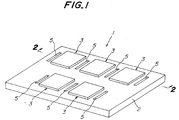
- the piezoelectric device 1 includes a locally thin-walled ceramic substrate 2 and a plurality of piezoelectric transducers 3 arranged on the upper surface of the substrate 2. More particularly, the substrate 2 has a plurality of thin-walled regions 2a and the piezoelectric transducers 3 are arranged on the thin-walled regions 2a.
- the substrate 2 has a plurality of closed cavities 4 therein, each defined by a closure wall 2b on the lower surface side of the substrate 2, peripheral walls 2c in the substrate 2 and a bottom wall on the upper surface side of the substrate 2, of which the bottom wall is constituted by the thin-walled region 2a of the substrate 2.
- the bottom wall 2a functions as a diaphragm of the piezoelectric transducer 3 in operation of the device 1.
- the substrate 2 has relatively thick-walled regions 2d adjacent to the thin-walled regions 2a, where it is formed with grooves 5 each arranged to extend along the peripheral wall 2c of the cavity 4 and to open at the upper surface of the substrate 2.
- the piezoelectric transducers 3 may be formed integrally with the substrate 2 by an ordinary film-formation process to be more fully described hereinafter, wherein a lower electrode layer 3a, a film-shaped-piezoelectric layer 3b and an upper electrode layer 3c are sequentially laminated one above the other. As further shown in Figs.
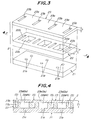
- the substrate 2 may be formed by known lamination process, wherein a lower green sheet 21 providing the closure wall 2b of the substrate 2, an intermediate green sheet 22 formed with window-like openings 22a corresponding to the cavity 4, and a thin-walled upper green sheet 23 providing the bottom wall 2a of the cavity 4, are sequentially laminated one above the other and subjected to a sintering to form an integrated substrate 2 (Fig. 4).
- the particulars of the three green sheets 21, 22, 23 forming the integrated substrate 2 will be explained below, with reference to Figs. 3 and 4.
- the upper green sheet 23 has flat regions 23a corresponding to the bottom walls 2a of the substrate 2, and slit-like openings 23b extending through the upper green sheet 23 in the direction of its thickness.
- the intermediate green sheet 22 has, besides the window-like openings 22a, slit-like grooves 22b with their bottoms situated close to the lower green sheet 21.
- the upper green sheet 23 and the intermediate green sheet 22 are superimposed with each other so that the slit-like openings 23b in the upper green sheet 23 and the slit-like grooves 22b in the intermediate green sheet 22 are brought into alignment with each other to form the groove 5 in the substrate 2.
- the lower green sheet 21 may have through-holes 21a to be used as an inlet which is in communication with an ink reservoir and/or as an outlet which is in communication with a discharge nozzle.
- the groove 5 in the substrate 2 has a length L which is at least 1/8, preferably 1/4 or more, of the length of the longitudinal edge of the cavity 4. Furthermore, as shown in Fig. 2A, the groove 5 has a depth D1 which is substantially same as, or greater than the thickness t of the thin-walled bottom wall 2a of the cavity 4, and which preferably satisfies the following equation (1): D1 ⁇ (t + D2/3) where D2 is the depth of the cavity 4. More preferably, the depth D1 of the groove 5 satisfies the following equation (2): D1 ⁇ (t + 2 ⁇ D2/3)
- the groove 5 has a width W1 as also shown in Fig. 2A, which is determined such that the width W2 of the thick-walled region 2d measured between the side wall of the groove 5 and the opposite peripheral wall 2c of the cavity 4 is within a range between 20 ⁇ m and 200 ⁇ m, preferably between 20 ⁇ m and 100 ⁇ m.
- the width W2 of the thick-walled region 2d is less than 20 ⁇ m, the stiffness of the thick-walled region 2d is often excessively lowered, making it difficult to effectively induce the desired vertical displacement of the bottom wall 2a of the cavity 4 and thereby achieve an efficient voluminal change of the cavity 4.
- the width W2 of the thick-walled region 2d is more than 200 ⁇ m, it becomes often difficult to achieve a sufficient stress relaxation during firing of the piezoelectric film layer, and hence to effectively improve the properties of the piezoelectric material.
- due to the increased stiffness of the thick-walled region 2d it becomes difficult to achieve a sufficient lateral displacement of the peripheral wall 2c of the cavity 4 thereby to enable a large voluminal change of the cavity 4.
- width W2 is applicable also when two or more grooves 5 are formed in each thick-walled region 2d of the substrate 2.
- the grooves 5 may have a square cross-section as shown in Figs. 2A and 4, or other appropriate cross-section such as V-shaped or trapezoid cross-section.
- the thin-walled region 2a of the substrate 2 i.e., the bottom wall of the cavity 4, which functions as the diaphragm of the piezoelectric transducer 3, in order to provide an improved high-speed response characteristic and a high conversion efficiency of the transducer 3, the thin-walled region 2a has a thickness which is preferably 50 ⁇ m or less, more preferably 30 ⁇ m or less, and further more preferably 10 ⁇ m or less.
- the piezoelectric device 1 includes groove 5 in the relatively thick-walled region 2d of the substrate 2 adjacent to and surrounding the peripheral wall 2c of the cavity 4. It is therefore possible to provide a higher compliance of the relatively thick-walled substrate region 2d adjacent to the peripheral wall 2c of the cavity 4, with which the thin-walled regions 2a of the substrate 2 can be readily deformed upon firing shrinkage during manufacture of the device 1.
- This means that the transducer 3 during manufacture of the device 1 can be subjected to the firing shrinkage in a relatively unrestricted sense, thereby minimizing the residual stresses in the transducer 3 and assuring a highly improved operational characteristics of the device 1.
- improved characteristics of the transducer 3, including the relative dielectric constant and to more fully make use of material properties which are inherent to the piezoelectric material.
- the piezoelectric device 1 when the piezoelectric device 1 according to the present invention includes an array of piezoelectric transducers 3 formed on a common substrate 2, the grooves 5 formed in the relatively thick-walled regions 2d of the substrate 2 and situated between the adjacent transducers 3 provide a low vibration transmissibility of the substrate 2 between the adjacent transducers 3.
- the grooves 5 thus serve to effectively eliminate or suppress undesirable interaction or crosstalk between adjacent transducers 3, and to make it readily possible for the thin-walled regions 2a of the substrate 2 to achieve a uniform amount of the desired vertical displacement.
- the groove 5 serves to absorb tensile forces between the transducers to thereby minimize the fluctuation in the vertical displacement amounts of the diaphragms.
- FIGs. 5A and 5B schematically illustrate the operation of the piezoelectric device according to the above-mentioned U.S. Patent No. 5,210,455, which is provided with a plurality of piezoelectric transducers 31, 32 on a ceramic substrate 2 having open cavities 4 which are not closed by a closure wall on the lower surface side of the substrate 2.
- the present invention thus provides a unique solution for the above-mentioned problems, by forming at least one groove 5 in the thick-walled region 2d of the ceramic substrate 2.
- FIGs. 6A, 6B and 6C A second embodiment of the unimorph-type piezoelectric device according to the present invention is shown in Figs. 6A, 6B and 6C, which is similar to, and directly comparable with the known device shown in Figs. 5A and 5B, in that the substrate 2 has open cavities 4. Formation of the grooves 5 in the thick-walled regions 2d of the substrate 2 makes it possible to provide a higher compliance of the diaphragm 2a and a resultant increased amount of its vertical displacement in operation of the device. As can be appreciated from Figs.
- the grooves 5 between adjacent transducers serve to effectively suppress interaction or crosstalk between the transducers, and the vertical displacement amount of the diaphragm 2a can be uniformly maintained substantially uninfluenced by the operational state of the device, i.e., regardless of whether one transducer only is actuated (Fig. 6B) or adjacent transducers are simultaneously actuated (Fig. 6C).
- FIG. 7 A third embodiment of the unimorph-type piezoelectric device according to the present invention is shown in Fig. 7, in which each thick-walled region 2d of the substrate 2 is relatively wide and formed with two grooves 5a, 5b of which the depth is greater than the thickness of the bottom wall 2a of the cavity 4.
- This embodiment effectively provides an improved compliance of the diaphragm 2a of the piezoelectric transducer 3, particularly when a plurality of transducers 3 are arranged on the substrate 2 with a relatively wide pitch.
- FIG. 8 and 9 A fourth embodiment of the unimorph-type piezoelectric device according to the present invention is shown in Figs. 8 and 9, which is also provided with the grooves 5 in the thick-walled regions 2d of the substrate 2.
- This embodiment is similar to the device disclosed in the applicants' copending U.S. Patent Application No. 08/206,939 or European Patent Application No. 94 301 633.7, of which the disclosure is here incorporated by reference.
- the piezoelectric device 1 includes piezoelectric transducers 3 of which the piezoelectric layer 3b has a dimension which is sufficient to substantially completely cover the lower electrode layer 3a.
- the piezoelectric layer 3b has at least one edge 11 in the form of an extension protruding beyond the lower electrode layer 3a, which is at least locally incompletely bonded to the ceramic substrate 2, as shown at 12.
- the term 'incomplete bond refers to a specific bonded state between the ceramic substrate 2 and at least one edge 11 of the piezoelectric layer 3b, which allows the piezoelectric layer 3b to undergo a substantially unrestricted movement relative to the substrate 2.
- buffer resin layers 13 Adjacent to the edges 11 of the piezoelectric layer 3b, there may be provided buffer resin layers 13 between the upper electrode layer 3c and the substrate 2, so as to provide a smooth and flexible connection of the upper electrode layer 3c to the substrate 2 and thereby protect the upper electrode layer 3c from possible damages due to impact or vibration during the production of the device or in the use condition.
- the above-mentioned arrangement of the piezoelectric device 1 shown in Figs. 8 and 9 makes it readily possible to manufacture the piezoelectric device with an improved productivity, because it is not necessary to precisely align the edges of the piezoelectric layer 3b with those of the lower electrode layer 3a.
- the edges 11 of the piezoelectric layer 3b of the device 1 shown in Figs. 8 and 9 serve to avoid short-circuit between the lower and upper electrode layers 3a, 3c.
- the incompletely bonded regions 12 between the ceramic substrate 2 and the edge 11 of the piezoelectric layer 3b protruding beyond the lower electrode layer 3a allows the piezoelectric layer 3b to be moved relative to the substrate 2 in an unrestricted sense. It is thus possible to achieve satisfactory reliability and functions of the device, e.g., generation of large force or displacement, or of high output voltage level.
- the present invention may also be applied to a piezoelectric device which includes a single piezoelectric transducer formed on the substrate.
- formation of the grooves in the thick-walled regions of the substrate adjacent to the thin-walled bottom wall of the cavity serve to provide a higher compliance of the bottom wall and hence significantly improved operational characteristics of the device.
- the substrate 2 preferably comprises zirconium oxide as a main component, having a crystal phase that has been completely or partially stabilized preferably by the addition of at least one compound selected from a group consisting of yttrium oxide, cerium oxide, magnesium oxide and calcium oxide.
- the amount of the additives required for partially or completely stabilizing the zirconium oxide as described above may be 1-30 mol% for yttrium oxide, 6-50 mol% for cerium oxide, and 5-40 mol% for the magnesium oxide and calcium oxide.
- the amount is preferably 2-7 mol%, more preferably 2-4 mol%, because the zirconium oxide added with the yttrium oxide of such amount has a partially stabilized crystal phase and thus exhibits particularly excellent substrate characteristics.
- a preferred method of forming the ceramic substrate 2 with at least one cavity is to prepare a first green sheet having a desired thickness and at least one window-like opening formed by using a suitable mold, punching with a suitable die, or machining process, such as ultrasonic machining.
- a second, relatively thin green sheet is further prepared to have a thickness which corresponds to that of the thin-walled region of the substrate. The second green sheet is superimposed on the first green sheet under predetermined temperature/pressure condition, and then fired and integrated with each other.
- the material for the ceramic substrate 2 may contain a sintering aid, such as clay or the like.
- a sintering aid such as clay or the like.
- the cavity 4 for defining the thin-walled region 2a has a generally square contour
- the cavity 4 it is advantageous for the cavity 4 to have dimensions which are determined such that the length of the cavity is 2-20 times larger than its width.
- the transducer 3 is formed on the thin-walled region 2a of the substrate 2 over an area which preferably corresponds to 50-95% of the width of the cavity 4.
- the ceramic substrate 2 which has been formed as explained above permits satisfactory operational characteristics of the piezoelectric transducer 3 formed thereon, it is advantageous to control the surface roughness Ra of the substrate 2 to be within a range of 0.03-0.9 ⁇ m. In this instance, the distortion or stress occurring in the piezoelectric transducer 3 can be effectively transmitted to the substrate 2 having the above-mentioned range of the surface roughness Ra, and vice versa. Such a control of the surface roughness Ra is also effective to assure a high mechanical strength of the relatively thin substrate.
- the green sheet for the ceramic substrate 2 may be subjected to sintering at a temperature of 1,000°C to 1,800°C prior to formation of the piezoelectric transducer 3.
- the green sheet for the ceramic substrate 2 may be subjected to a suitable film-formation process to form the piezoelectric transducer 3 and then sintered. Formation of the piezoelectric transducer 3 on the previously sintered ceramic substrate 2 is often desirable in view of minimization of warp in the final product and dimensional accuracy of the piezoelectric transducer 3.
- the groove 5 in the thick-walled region 2d of the substrate 2 may be formed either in the green sheet before the sintering step or in the already sintered substrate, by various methods.
- the groove may be formed in the sintered substrate by an appropriate process such as laser beam process, electron beam process, slicing, blasting and ultrasonic process.
- the groove may be formed in the green sheet by press or punching with a suitable die.
- the groove formation process may be carried out either before or after the formation of the film-type piezoelectric transducer.
- the laser beam process is particularly suitable in that formation of grooves with a relatively complicated shape can be carried out in a facilitated manner.
- a suitable laser is a Nd-YAG laser having a Gaussian or normal energy distribution in the beam and using a TEM 00 single mode resonance.
- the laser beam process is performed by controlling the laser beam width to be 140 ns or less, preferably 100 ns or less, by carrying out a pulsation control by means of a Q-switch at a frequency of 3.6 kHz, for example, by concentrating the laser beam diameter to be 50 ⁇ m or less, preferably within a range of 5-10 ⁇ m, by means of an apropriate concentration lens system, and by performing the process at a speed of 50 mm/sec or less.
- the piezoelectric transducer 3 on the ceramic substrate 2 comprising the electrode layers 3a, 3c and the piezoelectric layer 3b may be formed by a suitable film-formation process known, per se. That is to say, the film-fotmation process which may be applied to form the piezoelectric transducer 3 of the device 1 according to the present invention includes a thick-film formation process such as screen printing, spraying, dipping or coating, and a thin-film formation process such as ion beam method, sputtering, vacuum vapor deposition, ion plating, chemical vapor deposition (CVD) or plating. In particular, the thick-film formation process can be advantageously applied to form a film-like piezoelectric layer.
- a suitable film-formation process known, per se. That is to say, the film-fotmation process which may be applied to form the piezoelectric transducer 3 of the device 1 according to the present invention includes a thick-film formation process such as screen printing, spraying, dipping or coating
- the thick-film formation process makes it readily possible to form a film on the ceramic substrate by using a paste or slurry whose major component is powder of piezoelectric ceramic material.
- the powder of piezoelectric ceramic material has an average particle size within a range of 0.01 ⁇ m to 5 ⁇ m, preferably 0.05 ⁇ m to 3 ⁇ m, it is readily possible to realize excellent operational characteristics of the piezoelectric device.
- the pattern of such a film may be formed by screen printing method or photolithography method, the pattern may also be formed by removing unnecessary regions of the film by laser cutting, slicing, ultrasonic machining or other suitable machining process.
- the present invention is not limited to the specific construction, shape and/or pattern of the piezoelectric transducer illustrated in the drawings.
- the transducer may have triangular, rectangular or other polygonal shape, circular, elliptical or annular shape, comb- or lattice-like pattern, or any combination of these shapes and/or patterns.
- the electrode layers 3a, 3c and the piezoelectric layer 3b formed on the ceramic substrate 2 by a selected method as explained above may be either heat-treated in different steps for integration with the substrate each time a layer has been formed on the substrate, or simultaneously heat-treated in a single step for integration with the substrate after all the layers have been formed into a laminated structure on the substrate.
- these methods are applied to manufacture the piezoelectric device as shown in Figs. 8 and 9, it is possible to incompletely bond the edges of the piezoelectric layer 3b to the ceramic substrate 2.
- a film-formation process is used to form the electrode layers on the substrate or piezoelectric layer, it is not always a prerequisite condition to carry out the heat-treatment for integrating the film layers with the substrate or piezoelectric layer.
- the upper electrode layer 3c is preferably formed by a process which does not require heat-treatment.
- the heat treatment temperature suitable for integrating the film layers 3a, 3b, 3c of the piezoelectric transducer 3 and the ceramic substrate 2 is generally within a range of 900-1,400°C, preferably 1,000-1,400°C.
- the heat-treatment is preferably performed while controlling the atmosphere by heating the vaporization source of the piezoelectric material as well. It is also advantageous to use a method of firing the piezoelectric film layer while it is covered by a suitable cover member for preventing a direct exposure of the piezoelectric film layer to the firing atmosphere.
- the cover member consists preferably of a material which is similar to the ceramic substrate material.
- the lower and upper electrode layers 3a, 3c of the piezoelectric transducer 3 may be formed of any electrically conductive material which can withstand the oxidizing firing and the heat-treatment atmosphere at a considerably high temperature condition as explained above.
- the electrode layers may be formed of a single metal, an alloy of metals, a mixture of metal or alloy with an electrically insulating ceramic material, e.g., TiO2, Al2O3, ZrO2, etc., or an electrically conductive ceramic material.
- an electrode material whose major component is a noble metal having a high melting point, such as platinum, palladium, or rhodium, or an alloy such as silver-palladium, silver-platinum, platinum-palladium or the like.
- cermet material of platinum and the ceramic material for the substrate it is more preferable to use a cermet material of platinum and the ceramic material for the substrate, a cermet material of platinum and the ceramic material for the substrate and the piezoelectric material for the piezoelectric film layer, in view of an improved adhesion of the electrode layers to the piezoelectric film layer and/or the ceramic substrate.
- a material having a major component which comprises a platinum it is more preferable to use a material having a major component which comprises a platinum.
- the amount of the substrate material to be added to the electrode material is preferably 5-30% by volume, and the amount of the piezoelectric material to be added to the electrode material is preferably 5-20% by volume.
- the electrode layers 3a, 3c consisting of a conductive material as mentioned above may have a thickness of 20 ⁇ m or less, preferably 5 ⁇ m or less.
- the piezoelectric layer 3b may be formed of any piezoelectric material which exhibits a relatively large amount of field-induced strain or displacement when applied with a voltage, due to the piezoelectric effect.
- the piezoelectric material may be either a crystalline material or an amorphous material, and may be a semi-conductive material or a dielectric or ferroelectric ceramic material. Furthermore, the piezoelectric material may either require an initial polarization or poling treatment or may not require such treatment.
- the piezoelectric materials which can be used in the present invention has a composition whose major component is lead zirconate titanate (PZT), lead magnesium niobate (PMN), lead nickel niobate (PNN), lead manganese niobate, lead antimony stannate, lead zinc niobate, lead titanate, lead zirconate or a mixture or solid solution thereof.
- PZT lead zirconate titanate
- PMN lead magnesium niobate
- PNN lead nickel niobate
- lead manganese niobate lead antimony stannate
- lead zinc niobate lead titanate
- lead zirconate or a mixture or solid solution thereof.
- the piezoelectric materials indicated above whose major component is PZT or the like, may be added with a suitable amount of additives comprising an oxide or compound of lanthanum, barium, niobium, zinc, cerium, cadmium, chromium, cobalt, antimony, iron, yttrium, tantalum tungsten, nickel, manganese, lithium, strontium, calcium, and/or bismuth, so as to obtain a material whose major component is PLZT.
- additives comprising an oxide or compound of lanthanum, barium, niobium, zinc, cerium, cadmium, chromium, cobalt, antimony, iron, yttrium, tantalum tungsten, nickel, manganese, lithium, strontium, calcium, and/or bismuth, so as to obtain a material whose major component is PLZT.
- vitrous material such as silicon oxide
- lead contained in the piezoelectric materials such as PZT tends to react with the vitrous material, making it difficult to achieve a desired composition of the piezoelectric film layer, thereby causing undesirable fluctuation and deterioration of the operational characteristics of the piezoelectric device.
- piezoelectric materials indicated above it is preferable to use material of which the major component comprises a mixture of lead magnesium niobate, lead zirconate and lead titanate, or a mixture of lead nickel niobate, lead magnesium niobate, lead zirconate and lead titanate. It is particularly advantageous to use a piezoelectric material of which the major component comprises a mixture of lead magnesium niobate, lead zirconate and lead titanate. Such a piezoelectric material has a particularly low reactivity with the substrate material during the heat-treatment, and is thus free from segregation of its components. Therefore, a suitable treatment for maintaining the composition serves to readily realize a desired composition or crystal structure.
- a piezoelectric material has a particularly high piezoelectric constant, and can be used as a material suitable for forming the piezoelectric film layer by the above-mentioned thick-film formation process such as screen printing, spraying, dipping, coating and the like.
- a three-component material composed of lead magnesium niobate, lead zirconate and lead titanate which can be suitably used in the invention, preferably has a composition in the vicinity of phase boundaries of a pseudo-cubic crystal phase, a tetragonal crystal phase and a rhombohedral crystal phase.
- a composition containing 15-50 mol% of lead magnesium niobate, 10-45 mol% of lead zirconate and 30-45 mol% of lead titanate it is particularly advantageous to use a composition containing 15-50 mol% of lead magnesium niobate, 10-45 mol% of lead zirconate and 30-45 mol% of lead titanate.
- the piezoelectric transducer comprising the electrode layers 3a, 3c and the piezoelectric film layer 3b described above generally has a thickness of 100 ⁇ m or less.
- the piezoelectric film layer 3b has a thickness which is preferably 50 ⁇ m or less, more preferably within a range of 3-40 ⁇ m.
- Comparative sample S1 has open cavities such as that shown in Figs. 5A and 5B, and does not include grooves in the thick-walled regions of the substrate.
- Comparative sample S2 has closed cavities closed by a closure wall such as that shown in Figs. 2A and 2B, and does not include grooves in the thick-walled regions of the substrate.
- Comparative sample S3 has open cavities and includes shallow grooves in the thick-walled regions of the substrate, wherein each groove is arranged between adjacent transducers and has a depth which is substantially same as the thickness of the thin-walled region of the substrate.
- Sample of the invention S4 has closed cavities and include grooves in the thick-walled regions of the substrate, as shown in Figs. 2A and 2B, wherein each groove is arranged between adjacent transducers and has a depth of 100 ⁇ m which is greater than the thickness of the thin-walled region of the substrate.
- Sample of the invention S5 has closed cavities and include grooves in the thick-walled regions of the substrate, as shown in Figs. 2A and 2B, wherein each groove is arranged between adjacent transducers and has a depth of 50 ⁇ m which is greater than the thickness of the thin-walled region of the substrate.
- Sample of the invention S6 has closed cavities and include grooves in the thick-walled regions of the substrate, wherein two grooves are arranged between adjacent transducers as shown in Fig. 7, each having a depth of 100 ⁇ m which is greater than the thickness of the thin-walled region of the substrate.
- Each sample includes a substrate comprising a layer forming the peripheral wall of the cavity and having a thickness of 150 ⁇ m, which may be combined with a closure wall of a thickness of 150 ⁇ m, wherein the thickness of the thin-walled region is 10 ⁇ m.
- the vertical displacement amount achieved by the center transducer 3C of the sample S4 is higher than that achieved by the center transducer 3C of the comparative sample S2.
- the vertical displacement amount achieved by the center transducer 3C of the sample S4 is substantially as high as that achieved by the center transducer 3C of the comparative sample S1.
- the transducer of the sample S4 according to the invention exhibits the highest relative dielectric constant. This is believed due to the minimized residual stresses in the piezoelectric film layer and improved material characteristics thereof, both realized by the formation of the grooves in the thick-walled regions of the substrate and the resultant increased compliance of the thin-walled regions.
- Table 2 shows the reduced displacement rate D red (%) for each transducers of the samples S1 to S6.
- a greater depth of the groove serves to more effectively suppress the interaction or crosstalk between adjacent piezoelectric transducers.
- formation of two grooves between adjacent transducers results in even more effective suppression of the interaction or crosstalk between adjacent piezoelectric transducers.
- the piezoelectric device features the formation of at least one groove in the relatively thick-walled region of the substrate adjacent to and surrounding the peripheral wall of the cavity. It is thus possible to provide a higher compliance of the relatively thick-walled substrate region adjacent to the peripheral wall of the cavity, with which the thin-walled regions of the substrate can be readily deformed upon firing shrinkage during manufacture of the device. Therefore, despite the difference in the coefficient of thermal expansion of the materials for the substrate and the piezoelectric transducer, the transducer during manufacture of the device can be subjected to the firing shrinkage in a relatively unrestricted sense, thereby minimizing the residual stresses in the transducer and assuring a highly improved operational characteristics of the device.
- the piezoelectric device according to the present invention includes an array of piezoelectric transducers formed on a common substrate
- the grooves in the relatively thick-walled region of the substrate serves to effectively eliminate or suppress interaction or crosstalk between the transducers, and makes it readily possible to uniformly achieve a desired amount of displacement of the thin-walled regions of the substrate in a direction perpendicular to the general surface of the substrate.
Landscapes
- Engineering & Computer Science (AREA)
- Manufacturing & Machinery (AREA)
- Particle Formation And Scattering Control In Inkjet Printers (AREA)
- Piezo-Electric Transducers For Audible Bands (AREA)
Applications Claiming Priority (2)
| Application Number | Priority Date | Filing Date | Title |
|---|---|---|---|
| JP16394593A JP3318687B2 (ja) | 1993-06-08 | 1993-06-08 | 圧電/電歪膜型素子及びその製造方法 |
| JP163945/93 | 1993-06-08 |
Publications (2)
| Publication Number | Publication Date |
|---|---|
| EP0629007A1 true EP0629007A1 (de) | 1994-12-14 |
| EP0629007B1 EP0629007B1 (de) | 1997-03-05 |
Family
ID=15783811
Family Applications (1)
| Application Number | Title | Priority Date | Filing Date |
|---|---|---|---|
| EP94304112A Expired - Lifetime EP0629007B1 (de) | 1993-06-08 | 1994-06-08 | Piezoelektrische Anordnung |
Country Status (6)
| Country | Link |
|---|---|
| US (1) | US6584660B1 (de) |
| EP (1) | EP0629007B1 (de) |
| JP (1) | JP3318687B2 (de) |
| DE (1) | DE69401855T2 (de) |
| HK (1) | HK117197A (de) |
| SG (1) | SG66279A1 (de) |
Cited By (15)
| Publication number | Priority date | Publication date | Assignee | Title |
|---|---|---|---|---|
| EP0725451A1 (de) * | 1995-02-06 | 1996-08-07 | Thomson-Csf | Wandler aus elektromechanisch transformierendem Material, Mikroantrieb mit diesem Wandler und Verfahren zur Herstellung |
| EP0742596A1 (de) * | 1995-05-08 | 1996-11-13 | Ngk Insulators, Ltd. | Membranstruktur |
| EP0718900A3 (de) * | 1994-12-21 | 1998-03-11 | Ngk Insulators, Ltd. | Piezoelektrisches/elektrostriktives Dünnfilmelement mit einem Membran mit mindestens einem spannungsaufnemenden Gebiet am Rande |
| US5889352A (en) * | 1995-10-13 | 1999-03-30 | Ngk Insulators, Ltd. | Piezo-electric/electrostrictive film type element |
| US5898255A (en) * | 1995-07-28 | 1999-04-27 | Sony Corporation | Piezoelectric actuator and method for manufacturing |
| EP0926746A2 (de) * | 1997-12-25 | 1999-06-30 | Kyocera Corporation | Piezoelektrisches Antriebelement und damit ausgestatteter Tintenstrahldruckkopf |
| EP1089355A2 (de) * | 1999-10-01 | 2001-04-04 | Ngk Insulators, Ltd. | Piezoelektrisches/elektrostriktives Bauelement |
| WO2002073710A1 (fr) * | 2001-03-12 | 2002-09-19 | Ngk Insulators,Ltd. | Actionneur a films piezo-electriques/electrostrictifs et son procede de fabrication |
| US6495945B2 (en) * | 2000-09-11 | 2002-12-17 | Ngk Insulators, Ltd. | Piezoelectric/electrostrictive element |
| EP1387416A2 (de) * | 2002-07-26 | 2004-02-04 | Ngk Insulators, Ltd. | Piezoelektrisches/elektrostriktives filmartiges Bauelement |
| EP1529642A1 (de) * | 2003-11-05 | 2005-05-11 | Xerox Corporation | Tintenstrahlgerät |
| US6915547B2 (en) | 1999-10-01 | 2005-07-12 | Ngk Insulators, Ltd. | Piezoelectric/electrostrictive device and method of manufacturing same |
| US7164221B1 (en) | 1999-10-01 | 2007-01-16 | Ngk Insulators, Ltd. | Piezoelectric/electrostrictive device and method of manufacturing same |
| EP1842676A2 (de) * | 2006-04-06 | 2007-10-10 | Océ-Technologies B.V. | Druckkopf und Tintenstrahldrucker mit einem derartigen Druckkopf |
| WO2013079369A1 (en) * | 2011-11-30 | 2013-06-06 | Oce-Technologies B.V. | Inkjet print head and method for manufacturing such print head |
Families Citing this family (65)
| Publication number | Priority date | Publication date | Assignee | Title |
|---|---|---|---|---|
| US6335586B1 (en) * | 1998-12-28 | 2002-01-01 | Ngk Insulators, Ltd. | Piezoelectric/electrostrictive device and production method thereof |
| JP2000348321A (ja) * | 1999-06-03 | 2000-12-15 | Nec Corp | 磁気ディスク装置,磁気ヘッド,磁気ヘッドの製造方法および磁気ディスク装置の製造方法 |
| JP4032283B2 (ja) * | 2000-03-27 | 2008-01-16 | 富士フイルム株式会社 | マルチノズルインクジェットヘッド及びその製造方法 |
| JP3768789B2 (ja) * | 2000-09-07 | 2006-04-19 | アルプス電気株式会社 | 超音波振動子及びウエット処理用ノズル並びにウエット処理装置 |
| EP1340970A4 (de) * | 2000-11-06 | 2007-06-27 | Jtekt Corp | Sensorelement für eine mechanische grösse, lastsensorelement, beschleunigungssensorelement und drucksensorelement |
| US6794723B2 (en) * | 2001-09-12 | 2004-09-21 | Ngk Insulators, Ltd. | Matrix type piezoelectric/electrostrictive device and manufacturing method thereof |
| JP3908512B2 (ja) * | 2001-11-16 | 2007-04-25 | セイコーインスツル株式会社 | 圧電トランスデューサ及び脈波検出装置 |
| JP3991894B2 (ja) * | 2002-03-18 | 2007-10-17 | セイコーエプソン株式会社 | 圧電アクチュエータの製造方法、液体噴射ヘッドの製造方法、及び、アクチュエータ母部材 |
| JP3903936B2 (ja) * | 2002-03-18 | 2007-04-11 | セイコーエプソン株式会社 | 圧電素子、圧電アクチュエータ、及び、液体噴射ヘッド |
| US7019438B2 (en) * | 2002-06-21 | 2006-03-28 | Ngk Insulators, Ltd. | Piezoelectric/electrostrictive film device |
| US7067961B2 (en) * | 2002-07-12 | 2006-06-27 | Ngk Insulators, Ltd. | Piezoelectric/electrostrictive film device, and manufacturing method of the device |
| JP4447250B2 (ja) * | 2002-08-07 | 2010-04-07 | 日本碍子株式会社 | 圧電アクチュエータアレイ及び製造方法 |
| JP4422973B2 (ja) * | 2002-08-27 | 2010-03-03 | 京セラ株式会社 | 積層圧電体、アクチュエータ及び印刷ヘッド |
| US6987348B2 (en) * | 2002-12-13 | 2006-01-17 | Palo Alto Research Center Inc. | Piezoelectric transducers |
| US6967431B2 (en) * | 2002-12-13 | 2005-11-22 | Palo Alto Research Center Inc. | Piezoelectric transducers and methods of manufacture |
| US6843771B2 (en) * | 2003-01-15 | 2005-01-18 | Salutron, Inc. | Ultrasonic monitor for measuring heart rate and blood flow rate |
| US20060152375A1 (en) * | 2003-01-16 | 2006-07-13 | Matsushita Electric Industrial Co., Ltd. | Pressure-sensitive sensor and object detector |
| US7270404B2 (en) * | 2003-09-24 | 2007-09-18 | Fujifilm Corporation | Inkjet recording head, inkjet recording apparatus and method for manufacturing inkjet recording head |
| JP2005103771A (ja) * | 2003-09-26 | 2005-04-21 | Fuji Photo Film Co Ltd | インクジェットヘッドとその製造方法及びインクジェット記録装置 |
| JP2005104038A (ja) * | 2003-09-30 | 2005-04-21 | Fuji Photo Film Co Ltd | 吐出ヘッド及び液吐出装置 |
| US7375911B1 (en) * | 2003-11-25 | 2008-05-20 | Maxtor Corporation | Piezoelectric actuator and sensor for disk drive dual-stage servo systems |
| US7585061B2 (en) * | 2004-08-27 | 2009-09-08 | Fujifilm Corporation | Ejection head and image forming apparatus |
| JP4504237B2 (ja) * | 2005-03-18 | 2010-07-14 | 富士通株式会社 | ウエットエッチング方法、マイクロ可動素子製造方法、およびマイクロ可動素子 |
| US7449816B2 (en) * | 2005-03-25 | 2008-11-11 | Brother Kogyo Kabushiki Kaisha | Piezoelectric actuator, liquid transporting apparatus, and method for producing piezoelectric actuator and method for producing liquid transporting apparatus |
| JP4630998B2 (ja) * | 2005-05-31 | 2011-02-09 | 独立行政法人産業技術総合研究所 | スピーカ装置又はマイクロフォン装置 |
| US7535373B2 (en) * | 2005-07-15 | 2009-05-19 | Honeywell International, Inc. | Security techniques for electronic devices |
| JP4597105B2 (ja) * | 2005-09-12 | 2010-12-15 | 日本碍子株式会社 | スピーカ及び電力発生装置 |
| US20070120896A1 (en) * | 2005-11-30 | 2007-05-31 | Xerox Corporation | Drop generator |
| JP4618165B2 (ja) * | 2006-03-06 | 2011-01-26 | 株式会社デンソー | 超音波センサ |
| JP2007276479A (ja) * | 2006-04-06 | 2007-10-25 | Oce Technol Bv | プリントヘッド及びこれを含むインクジェットプリンタ |
| JP4091641B2 (ja) * | 2006-04-07 | 2008-05-28 | 富士フイルム株式会社 | 圧電素子とその製造方法、及びインクジェット式記録ヘッド |
| JP5223255B2 (ja) * | 2006-07-18 | 2013-06-26 | ブラザー工業株式会社 | 圧電アクチュエータ、液体移送装置、及び、液滴噴射装置 |
| US7608983B2 (en) * | 2006-07-18 | 2009-10-27 | Brother Kogyo Kabushiki Kaisha | Piezoelectric actuator, liquid transporting apparatus, and liquid-droplet jetting apparatus |
| US7950782B2 (en) * | 2006-12-21 | 2011-05-31 | Seiko Epson Corporation | Droplet discharging head, energy converter, piezoelectric device, MEMS structure, cantilever actuator, piezoelectric sensor, and piezoelectric linear motor |
| US7851970B2 (en) * | 2006-12-22 | 2010-12-14 | The Charles Stark Draper Laboratory, Inc. | Structures for crystal packaging including flexible membranes |
| US20080246367A1 (en) * | 2006-12-29 | 2008-10-09 | Adaptivenergy, Llc | Tuned laminated piezoelectric elements and methods of tuning same |
| US7786653B2 (en) * | 2007-07-03 | 2010-08-31 | Northrop Grumman Systems Corporation | MEMS piezoelectric switch |
| US7854497B2 (en) | 2007-10-30 | 2010-12-21 | Hewlett-Packard Development Company, L.P. | Fluid ejection device |
| US8379888B2 (en) * | 2008-01-18 | 2013-02-19 | National Taiwan University | Flexible piezoelectric sound-generating devices |
| CN101801671B (zh) * | 2008-03-26 | 2013-08-07 | 日本碍子株式会社 | 液滴吐出装置及液滴吐出装置的制造方法 |
| WO2010039343A1 (en) * | 2008-09-30 | 2010-04-08 | Fujifilm Corporation | Method for nozzle velocity control |
| JP2012504072A (ja) * | 2008-09-30 | 2012-02-16 | フジフィルム ディマティックス, インコーポレイテッド | ノズル流過速度の制御 |
| JP2010143205A (ja) * | 2008-12-22 | 2010-07-01 | Seiko Epson Corp | 液体噴射ヘッド及び液体噴射装置並びにアクチュエータ装置 |
| US8525279B2 (en) * | 2009-06-04 | 2013-09-03 | University Of Louisville Research Foundation, Inc. | Single element three terminal piezoresistive pressure sensor |
| KR101101467B1 (ko) * | 2009-07-28 | 2012-01-03 | 삼성전기주식회사 | 잉크젯 헤드 및 잉크젯 헤드의 제조 방법 |
| US8484823B2 (en) * | 2009-08-28 | 2013-07-16 | The Charles Stark Draper Laboratory, Inc. | Methods and apparatus for mounting a crystal |
| JP5754129B2 (ja) * | 2010-03-11 | 2015-07-29 | セイコーエプソン株式会社 | 圧電素子、圧電センサー、電子機器、および圧電素子の製造方法 |
| JP5677780B2 (ja) * | 2010-07-28 | 2015-02-25 | 日本セラミック株式会社 | 超音波送受信器 |
| KR20120080882A (ko) * | 2011-01-10 | 2012-07-18 | 삼성전자주식회사 | 음향 변환기 및 그 구동방법 |
| US20130342488A1 (en) * | 2012-06-26 | 2013-12-26 | Kent Displays Incorporated | Cholesteric liquid crystal writing tablet erased by a piezoelectric transducer |
| WO2014103593A1 (ja) * | 2012-12-26 | 2014-07-03 | 富士フイルム株式会社 | ユニモルフ型超音波探触子およびその製造方法 |
| WO2015131083A1 (en) | 2014-02-28 | 2015-09-03 | The Regents Of The University Of California | Variable thickness diaphragm for a wideband robust piezoelectric micromachined ultrasonic transducer (pmut) |
| JP2016033970A (ja) | 2014-07-31 | 2016-03-10 | セイコーエプソン株式会社 | 超音波デバイスおよびその製造方法並びにプローブおよび電子機器 |
| JP2017019168A (ja) * | 2015-07-09 | 2017-01-26 | 東芝テック株式会社 | インクジェットヘッドとその製造方法 |
| WO2018081439A1 (en) | 2016-10-27 | 2018-05-03 | Cts Corporation | Transducer, transducer array, and method of making the same |
| US11039814B2 (en) | 2016-12-04 | 2021-06-22 | Exo Imaging, Inc. | Imaging devices having piezoelectric transducers |
| CN110603817B (zh) * | 2017-05-09 | 2020-08-25 | 富士胶片株式会社 | 压电麦克风芯片及压电麦克风 |
| US10656007B2 (en) | 2018-04-11 | 2020-05-19 | Exo Imaging Inc. | Asymmetrical ultrasound transducer array |
| US10648852B2 (en) | 2018-04-11 | 2020-05-12 | Exo Imaging Inc. | Imaging devices having piezoelectric transceivers |
| EP3797412A4 (de) | 2018-05-21 | 2022-03-09 | Exo Imaging Inc. | Ultraschallwandler mit q-spoiling |
| US10699741B1 (en) * | 2019-01-08 | 2020-06-30 | International Business Machines Corporation | Multi-channel magnetic recording head having compliantly encapsulated transducers |
| US11794209B2 (en) | 2019-09-12 | 2023-10-24 | Exo Imaging, Inc. | Increased MUT coupling efficiency and bandwidth via edge groove, virtual pivots, and free boundaries |
| JP7517005B2 (ja) * | 2020-09-11 | 2024-07-17 | 株式会社リコー | 液体吐出ヘッドおよび液体を吐出する装置 |
| US11819881B2 (en) | 2021-03-31 | 2023-11-21 | Exo Imaging, Inc. | Imaging devices having piezoelectric transceivers with harmonic characteristics |
| US11951512B2 (en) | 2021-03-31 | 2024-04-09 | Exo Imaging, Inc. | Imaging devices having piezoelectric transceivers with harmonic characteristics |
Citations (2)
| Publication number | Priority date | Publication date | Assignee | Title |
|---|---|---|---|---|
| JPS60111600A (ja) * | 1983-11-21 | 1985-06-18 | Mitsubishi Mining & Cement Co Ltd | 電気機械変換素子 |
| EP0468796A1 (de) * | 1990-07-26 | 1992-01-29 | Ngk Insulators, Ltd. | Piezoelektrisches/elektrostriktives Antriebselement mit keramischem Substrat |
Family Cites Families (8)
| Publication number | Priority date | Publication date | Assignee | Title |
|---|---|---|---|---|
| JPS5942193A (ja) * | 1982-09-02 | 1984-03-08 | Toshiba Corp | レ−ザスクライビング方法 |
| US4551647A (en) * | 1983-03-08 | 1985-11-05 | General Electric Company | Temperature compensated piezoelectric transducer and lens assembly and method of making the assembly |
| US4641153A (en) * | 1985-09-03 | 1987-02-03 | Pitney Bowes Inc. | Notched piezo-electric transducer for an ink jet device |
| DE3630206A1 (de) * | 1985-09-06 | 1987-03-19 | Fuji Electric Co Ltd | Tintenstrahldruckkopf |
| JPH01188350A (ja) * | 1988-01-25 | 1989-07-27 | Fuji Electric Co Ltd | インクジェット記録ヘッドの製造方法 |
| JP2806386B2 (ja) * | 1988-02-16 | 1998-09-30 | 富士電機株式会社 | インクジェット記録ヘッド |
| DE68906001T2 (de) * | 1988-12-07 | 1993-09-09 | Seiko Epson Corp | Auf abruf arbeitender tintenstrahldruckkopf. |
| US5057664A (en) * | 1989-10-20 | 1991-10-15 | Electro Scientific Industries, Inc. | Method and apparatus for laser processing a target material to provide a uniformly smooth, continuous trim profile |
-
1993
- 1993-06-08 JP JP16394593A patent/JP3318687B2/ja not_active Expired - Lifetime
-
1994
- 1994-06-08 EP EP94304112A patent/EP0629007B1/de not_active Expired - Lifetime
- 1994-06-08 US US08/257,020 patent/US6584660B1/en not_active Expired - Fee Related
- 1994-06-08 DE DE69401855T patent/DE69401855T2/de not_active Expired - Lifetime
- 1994-06-08 SG SG1996007142A patent/SG66279A1/en unknown
-
1997
- 1997-06-26 HK HK117197A patent/HK117197A/xx not_active IP Right Cessation
Patent Citations (2)
| Publication number | Priority date | Publication date | Assignee | Title |
|---|---|---|---|---|
| JPS60111600A (ja) * | 1983-11-21 | 1985-06-18 | Mitsubishi Mining & Cement Co Ltd | 電気機械変換素子 |
| EP0468796A1 (de) * | 1990-07-26 | 1992-01-29 | Ngk Insulators, Ltd. | Piezoelektrisches/elektrostriktives Antriebselement mit keramischem Substrat |
Non-Patent Citations (1)
| Title |
|---|
| PATENT ABSTRACTS OF JAPAN vol. 009, no. 266 (E - 352) 23 October 1985 (1985-10-23) * |
Cited By (30)
| Publication number | Priority date | Publication date | Assignee | Title |
|---|---|---|---|---|
| EP0718900A3 (de) * | 1994-12-21 | 1998-03-11 | Ngk Insulators, Ltd. | Piezoelektrisches/elektrostriktives Dünnfilmelement mit einem Membran mit mindestens einem spannungsaufnemenden Gebiet am Rande |
| US5767612A (en) * | 1994-12-21 | 1998-06-16 | Ngk Insulators, Ltd. | Piezoelectric/electrostrictive film element with a diaphragm having at least one stress releasing end section |
| US5889353A (en) * | 1994-12-21 | 1999-03-30 | Ngk Insulators, Ltd. | Piezoelectric/electrostrictive film element with a diaphram having at least one stress releasing end section |
| CN1123939C (zh) * | 1994-12-21 | 2003-10-08 | 日本碍子株式会社 | 具有至少一个应力释放端部的压电/电致伸缩膜元件 |
| US5940947A (en) * | 1994-12-21 | 1999-08-24 | Ngk Insulators, Ltd. | Method of making a piezoelectric/electrostrictive film element with a diaphragm having at least one stress releasing end section |
| EP0725451A1 (de) * | 1995-02-06 | 1996-08-07 | Thomson-Csf | Wandler aus elektromechanisch transformierendem Material, Mikroantrieb mit diesem Wandler und Verfahren zur Herstellung |
| FR2730362A1 (fr) * | 1995-02-06 | 1996-08-09 | Thomson Csf | Transducteur en materiau a transformation electromecanique, application a des microactionneurs et procede de realisation |
| EP0742596A1 (de) * | 1995-05-08 | 1996-11-13 | Ngk Insulators, Ltd. | Membranstruktur |
| US5965970A (en) * | 1995-05-08 | 1999-10-12 | Ngk Insulators, Ltd. | Diaphragm structure |
| US5898255A (en) * | 1995-07-28 | 1999-04-27 | Sony Corporation | Piezoelectric actuator and method for manufacturing |
| US6021552A (en) * | 1995-07-28 | 2000-02-08 | Sony Corporation | Method of manufacturing a piezoelectric actuator |
| US5889352A (en) * | 1995-10-13 | 1999-03-30 | Ngk Insulators, Ltd. | Piezo-electric/electrostrictive film type element |
| EP0926746A3 (de) * | 1997-12-25 | 2002-10-02 | Kyocera Corporation | Piezoelektrisches Antriebelement und damit ausgestatteter Tintenstrahldruckkopf |
| EP0926746A2 (de) * | 1997-12-25 | 1999-06-30 | Kyocera Corporation | Piezoelektrisches Antriebelement und damit ausgestatteter Tintenstrahldruckkopf |
| EP1089355A2 (de) * | 1999-10-01 | 2001-04-04 | Ngk Insulators, Ltd. | Piezoelektrisches/elektrostriktives Bauelement |
| US7336021B2 (en) | 1999-10-01 | 2008-02-26 | Ngk Insulators, Ltd. | Piezoelectric/electrostrictive device and method of manufacturing same |
| EP1089355A3 (de) * | 1999-10-01 | 2004-10-06 | Ngk Insulators, Ltd. | Piezoelektrisches/elektrostriktives Bauelement |
| US7164221B1 (en) | 1999-10-01 | 2007-01-16 | Ngk Insulators, Ltd. | Piezoelectric/electrostrictive device and method of manufacturing same |
| US6915547B2 (en) | 1999-10-01 | 2005-07-12 | Ngk Insulators, Ltd. | Piezoelectric/electrostrictive device and method of manufacturing same |
| US6495945B2 (en) * | 2000-09-11 | 2002-12-17 | Ngk Insulators, Ltd. | Piezoelectric/electrostrictive element |
| US7044586B2 (en) | 2001-03-12 | 2006-05-16 | Ngk Insulators, Ltd. | Piezoelectric/electrostrictive film type actuator and method of manufacturing the actuator |
| WO2002073710A1 (fr) * | 2001-03-12 | 2002-09-19 | Ngk Insulators,Ltd. | Actionneur a films piezo-electriques/electrostrictifs et son procede de fabrication |
| EP1387416A3 (de) * | 2002-07-26 | 2006-03-22 | Ngk Insulators, Ltd. | Piezoelektrisches/elektrostriktives filmartiges Bauelement |
| EP1387416A2 (de) * | 2002-07-26 | 2004-02-04 | Ngk Insulators, Ltd. | Piezoelektrisches/elektrostriktives filmartiges Bauelement |
| US7048361B2 (en) | 2003-11-05 | 2006-05-23 | Xerox Corporation | Ink jet apparatus |
| EP1529642A1 (de) * | 2003-11-05 | 2005-05-11 | Xerox Corporation | Tintenstrahlgerät |
| EP1842676A2 (de) * | 2006-04-06 | 2007-10-10 | Océ-Technologies B.V. | Druckkopf und Tintenstrahldrucker mit einem derartigen Druckkopf |
| EP1842676A3 (de) * | 2006-04-06 | 2009-06-17 | Océ-Technologies B.V. | Druckkopf und Tintenstrahldrucker mit einem derartigen Druckkopf |
| WO2013079369A1 (en) * | 2011-11-30 | 2013-06-06 | Oce-Technologies B.V. | Inkjet print head and method for manufacturing such print head |
| US8899732B2 (en) | 2011-11-30 | 2014-12-02 | Oce-Technologies B.V. | Inkjet print head having a pivotably supported membrane and method for manufacturing such a print head |
Also Published As
| Publication number | Publication date |
|---|---|
| HK117197A (en) | 1997-09-05 |
| JPH06350155A (ja) | 1994-12-22 |
| DE69401855D1 (de) | 1997-04-10 |
| US6584660B1 (en) | 2003-07-01 |
| SG66279A1 (en) | 1999-07-20 |
| JP3318687B2 (ja) | 2002-08-26 |
| DE69401855T2 (de) | 1997-07-31 |
| EP0629007B1 (de) | 1997-03-05 |
Similar Documents
| Publication | Publication Date | Title |
|---|---|---|
| EP0629007B1 (de) | Piezoelektrische Anordnung | |
| EP0615294B1 (de) | Piezoelektrische Anordnung | |
| EP0606767B1 (de) | Piezoelektrische Anordnung | |
| EP1148561B1 (de) | Piezoelektrische/elektrostriktive Film-Bauelemente sowie deren Herstellungsverfahren | |
| EP0782203B1 (de) | Piezoelektrisches/Elektrostriktives Element vom Dünnschicht-Typ und Verfahren zu seiner Herstellung | |
| EP0526048B1 (de) | Piezoelektrischer/elektrostriktiver Element mit einem keramischen Substrat aus stabilisiertem Zirkoniumdioxid | |
| EP0656665B1 (de) | Piezoelektrische Anordnung | |
| EP0468796B1 (de) | Piezoelektrisches/elektrostriktives Antriebselement mit keramischem Substrat | |
| EP0561616B1 (de) | Piezoelektrisches/elektrostriktives Element mit Hilfselektrode zwischen einer piezoelektrischen/elektrostriktiven Schicht und dem Substrat | |
| EP0718900B1 (de) | Piezoelektrisches/elektrostriktives Dünnfilmelement mit einem Membran mit mindestens einem spannungsaufnemenden Gebiet am Rande | |
| EP0667646A1 (de) | Piezoelektrisches/elektrostriktives Dünnfilmelement und Herstellungsverfahren | |
| EP0766325B1 (de) | Piezoeletrisches/elektrostriktives Dünnfilmelement und Herstellungsverfahren | |
| US6246156B1 (en) | Piezoelectric/electrostrictive element | |
| KR20020066226A (ko) | 압전 구조체, 액체 토출 헤드 및 그 제조 방법 | |
| JPH0549270A (ja) | 圧電/電歪アクチユエータ | |
| JP3282085B2 (ja) | 圧電/電歪膜型素子の製造方法 | |
| JP2003008096A (ja) | 圧電/電歪膜素子 |
Legal Events
| Date | Code | Title | Description |
|---|---|---|---|
| PUAI | Public reference made under article 153(3) epc to a published international application that has entered the european phase |
Free format text: ORIGINAL CODE: 0009012 |
|
| AK | Designated contracting states |
Kind code of ref document: A1 Designated state(s): DE FR GB IT |
|
| 17P | Request for examination filed |
Effective date: 19950316 |
|
| RAP1 | Party data changed (applicant data changed or rights of an application transferred) |
Owner name: SEIKO EPSON CORPORATION Owner name: NGK INSULATORS, LTD. |
|
| 17Q | First examination report despatched |
Effective date: 19960208 |
|
| GRAG | Despatch of communication of intention to grant |
Free format text: ORIGINAL CODE: EPIDOS AGRA |
|
| GRAH | Despatch of communication of intention to grant a patent |
Free format text: ORIGINAL CODE: EPIDOS IGRA |
|
| GRAH | Despatch of communication of intention to grant a patent |
Free format text: ORIGINAL CODE: EPIDOS IGRA |
|
| GRAA | (expected) grant |
Free format text: ORIGINAL CODE: 0009210 |
|
| AK | Designated contracting states |
Kind code of ref document: B1 Designated state(s): DE FR GB IT |
|
| REF | Corresponds to: |
Ref document number: 69401855 Country of ref document: DE Date of ref document: 19970410 |
|
| ITF | It: translation for a ep patent filed | ||
| ET | Fr: translation filed | ||
| PLBE | No opposition filed within time limit |
Free format text: ORIGINAL CODE: 0009261 |
|
| STAA | Information on the status of an ep patent application or granted ep patent |
Free format text: STATUS: NO OPPOSITION FILED WITHIN TIME LIMIT |
|
| 26N | No opposition filed | ||
| REG | Reference to a national code |
Ref country code: GB Ref legal event code: IF02 |
|
| PGFP | Annual fee paid to national office [announced via postgrant information from national office to epo] |
Ref country code: GB Payment date: 20130605 Year of fee payment: 20 Ref country code: DE Payment date: 20130605 Year of fee payment: 20 |
|
| PGFP | Annual fee paid to national office [announced via postgrant information from national office to epo] |
Ref country code: IT Payment date: 20130619 Year of fee payment: 20 Ref country code: FR Payment date: 20130624 Year of fee payment: 20 |
|
| REG | Reference to a national code |
Ref country code: DE Ref legal event code: R071 Ref document number: 69401855 Country of ref document: DE |
|
| REG | Reference to a national code |
Ref country code: DE Ref legal event code: R071 Ref document number: 69401855 Country of ref document: DE |
|
| REG | Reference to a national code |
Ref country code: GB Ref legal event code: PE20 Expiry date: 20140607 |
|
| PG25 | Lapsed in a contracting state [announced via postgrant information from national office to epo] |
Ref country code: GB Free format text: LAPSE BECAUSE OF EXPIRATION OF PROTECTION Effective date: 20140607 |
|
| PG25 | Lapsed in a contracting state [announced via postgrant information from national office to epo] |
Ref country code: DE Free format text: LAPSE BECAUSE OF EXPIRATION OF PROTECTION Effective date: 20140611 |