EP0627734A1 - Verfahren zur Herstellung eines optischen Aufzeichnungsmediums - Google Patents
Verfahren zur Herstellung eines optischen Aufzeichnungsmediums Download PDFInfo
- Publication number
- EP0627734A1 EP0627734A1 EP19940303670 EP94303670A EP0627734A1 EP 0627734 A1 EP0627734 A1 EP 0627734A1 EP 19940303670 EP19940303670 EP 19940303670 EP 94303670 A EP94303670 A EP 94303670A EP 0627734 A1 EP0627734 A1 EP 0627734A1
- Authority
- EP
- European Patent Office
- Prior art keywords
- recording medium
- optical recording
- adhesive layer
- substrate
- process according
- Prior art date
- Legal status (The legal status is an assumption and is not a legal conclusion. Google has not performed a legal analysis and makes no representation as to the accuracy of the status listed.)
- Withdrawn
Links
Images


Classifications
-
- B—PERFORMING OPERATIONS; TRANSPORTING
- B32—LAYERED PRODUCTS
- B32B—LAYERED PRODUCTS, i.e. PRODUCTS BUILT-UP OF STRATA OF FLAT OR NON-FLAT, e.g. CELLULAR OR HONEYCOMB, FORM
- B32B43/00—Operations specially adapted for layered products and not otherwise provided for, e.g. repairing; Apparatus therefor
-
- B—PERFORMING OPERATIONS; TRANSPORTING
- B26—HAND CUTTING TOOLS; CUTTING; SEVERING
- B26D—CUTTING; DETAILS COMMON TO MACHINES FOR PERFORATING, PUNCHING, CUTTING-OUT, STAMPING-OUT OR SEVERING
- B26D7/00—Details of apparatus for cutting, cutting-out, stamping-out, punching, perforating, or severing by means other than cutting
- B26D7/08—Means for treating work or cutting member to facilitate cutting
-
- G—PHYSICS
- G06—COMPUTING; CALCULATING OR COUNTING
- G06K—GRAPHICAL DATA READING; PRESENTATION OF DATA; RECORD CARRIERS; HANDLING RECORD CARRIERS
- G06K19/00—Record carriers for use with machines and with at least a part designed to carry digital markings
- G06K19/06—Record carriers for use with machines and with at least a part designed to carry digital markings characterised by the kind of the digital marking, e.g. shape, nature, code
- G06K19/06009—Record carriers for use with machines and with at least a part designed to carry digital markings characterised by the kind of the digital marking, e.g. shape, nature, code with optically detectable marking
- G06K19/06046—Constructional details
-
- G—PHYSICS
- G11—INFORMATION STORAGE
- G11B—INFORMATION STORAGE BASED ON RELATIVE MOVEMENT BETWEEN RECORD CARRIER AND TRANSDUCER
- G11B7/00—Recording or reproducing by optical means, e.g. recording using a thermal beam of optical radiation by modifying optical properties or the physical structure, reproducing using an optical beam at lower power by sensing optical properties; Record carriers therefor
- G11B7/24—Record carriers characterised by shape, structure or physical properties, or by the selection of the material
- G11B7/241—Record carriers characterised by shape, structure or physical properties, or by the selection of the material characterised by the selection of the material
- G11B7/252—Record carriers characterised by shape, structure or physical properties, or by the selection of the material characterised by the selection of the material of layers other than recording layers
- G11B7/256—Record carriers characterised by shape, structure or physical properties, or by the selection of the material characterised by the selection of the material of layers other than recording layers of layers improving adhesion between layers
-
- G—PHYSICS
- G11—INFORMATION STORAGE
- G11B—INFORMATION STORAGE BASED ON RELATIVE MOVEMENT BETWEEN RECORD CARRIER AND TRANSDUCER
- G11B7/00—Recording or reproducing by optical means, e.g. recording using a thermal beam of optical radiation by modifying optical properties or the physical structure, reproducing using an optical beam at lower power by sensing optical properties; Record carriers therefor
- G11B7/24—Record carriers characterised by shape, structure or physical properties, or by the selection of the material
- G11B7/26—Apparatus or processes specially adapted for the manufacture of record carriers
-
- B—PERFORMING OPERATIONS; TRANSPORTING
- B32—LAYERED PRODUCTS
- B32B—LAYERED PRODUCTS, i.e. PRODUCTS BUILT-UP OF STRATA OF FLAT OR NON-FLAT, e.g. CELLULAR OR HONEYCOMB, FORM
- B32B2429/00—Carriers for sound or information
-
- G—PHYSICS
- G11—INFORMATION STORAGE
- G11B—INFORMATION STORAGE BASED ON RELATIVE MOVEMENT BETWEEN RECORD CARRIER AND TRANSDUCER
- G11B7/00—Recording or reproducing by optical means, e.g. recording using a thermal beam of optical radiation by modifying optical properties or the physical structure, reproducing using an optical beam at lower power by sensing optical properties; Record carriers therefor
- G11B7/24—Record carriers characterised by shape, structure or physical properties, or by the selection of the material
- G11B7/241—Record carriers characterised by shape, structure or physical properties, or by the selection of the material characterised by the selection of the material
- G11B7/242—Record carriers characterised by shape, structure or physical properties, or by the selection of the material characterised by the selection of the material of recording layers
- G11B7/244—Record carriers characterised by shape, structure or physical properties, or by the selection of the material characterised by the selection of the material of recording layers comprising organic materials only
- G11B7/246—Record carriers characterised by shape, structure or physical properties, or by the selection of the material characterised by the selection of the material of recording layers comprising organic materials only containing dyes
- G11B7/247—Record carriers characterised by shape, structure or physical properties, or by the selection of the material characterised by the selection of the material of recording layers comprising organic materials only containing dyes methine or polymethine dyes
- G11B7/2472—Record carriers characterised by shape, structure or physical properties, or by the selection of the material characterised by the selection of the material of recording layers comprising organic materials only containing dyes methine or polymethine dyes cyanine
-
- G—PHYSICS
- G11—INFORMATION STORAGE
- G11B—INFORMATION STORAGE BASED ON RELATIVE MOVEMENT BETWEEN RECORD CARRIER AND TRANSDUCER
- G11B7/00—Recording or reproducing by optical means, e.g. recording using a thermal beam of optical radiation by modifying optical properties or the physical structure, reproducing using an optical beam at lower power by sensing optical properties; Record carriers therefor
- G11B7/24—Record carriers characterised by shape, structure or physical properties, or by the selection of the material
- G11B7/241—Record carriers characterised by shape, structure or physical properties, or by the selection of the material characterised by the selection of the material
- G11B7/252—Record carriers characterised by shape, structure or physical properties, or by the selection of the material characterised by the selection of the material of layers other than recording layers
- G11B7/253—Record carriers characterised by shape, structure or physical properties, or by the selection of the material characterised by the selection of the material of layers other than recording layers of substrates
- G11B7/2533—Record carriers characterised by shape, structure or physical properties, or by the selection of the material characterised by the selection of the material of layers other than recording layers of substrates comprising resins
- G11B7/2534—Record carriers characterised by shape, structure or physical properties, or by the selection of the material characterised by the selection of the material of layers other than recording layers of substrates comprising resins polycarbonates [PC]
-
- G—PHYSICS
- G11—INFORMATION STORAGE
- G11B—INFORMATION STORAGE BASED ON RELATIVE MOVEMENT BETWEEN RECORD CARRIER AND TRANSDUCER
- G11B7/00—Recording or reproducing by optical means, e.g. recording using a thermal beam of optical radiation by modifying optical properties or the physical structure, reproducing using an optical beam at lower power by sensing optical properties; Record carriers therefor
- G11B7/24—Record carriers characterised by shape, structure or physical properties, or by the selection of the material
- G11B7/241—Record carriers characterised by shape, structure or physical properties, or by the selection of the material characterised by the selection of the material
- G11B7/252—Record carriers characterised by shape, structure or physical properties, or by the selection of the material characterised by the selection of the material of layers other than recording layers
- G11B7/254—Record carriers characterised by shape, structure or physical properties, or by the selection of the material characterised by the selection of the material of layers other than recording layers of protective topcoat layers
- G11B7/2542—Record carriers characterised by shape, structure or physical properties, or by the selection of the material characterised by the selection of the material of layers other than recording layers of protective topcoat layers consisting essentially of organic resins
-
- Y—GENERAL TAGGING OF NEW TECHNOLOGICAL DEVELOPMENTS; GENERAL TAGGING OF CROSS-SECTIONAL TECHNOLOGIES SPANNING OVER SEVERAL SECTIONS OF THE IPC; TECHNICAL SUBJECTS COVERED BY FORMER USPC CROSS-REFERENCE ART COLLECTIONS [XRACs] AND DIGESTS
- Y10—TECHNICAL SUBJECTS COVERED BY FORMER USPC
- Y10T—TECHNICAL SUBJECTS COVERED BY FORMER US CLASSIFICATION
- Y10T83/00—Cutting
- Y10T83/04—Processes
- Y10T83/0405—With preparatory or simultaneous ancillary treatment of work
- Y10T83/041—By heating or cooling
Definitions
- the present invention relates to a process for manufacturing an optical recording medium and, more particularly, to a process for manufacturing a high-quality optical recording medium.
- an optical recording medium is known to have a structure in which a recording film is formed on a substrate having a preformat on the surface thereof and a protective substrate is provided on the recording film through an adhesive layer, or in which a spacer is mounted in the inner and outer peripheries of a substrate by using an adhesive agent and a protective substrate is provided through the spacer.
- the above method (2) is preferable in that handling in manufacturing steps is easy.
- a cutting edge or a laser beam, a router and the like have been proposed for cutting.
- the cutting method using a cutting edge is preferable to reduce the cost of the optical recording medium.
- cutting using a cutting edge has the problem that an adhesive agent squeezes out in the cut end portion of the optical recording medium, as shown in Fig. 3. This tendency is conspicuous when a thermoplastic adhesive agent is used as an adhesive agent. Further, the squeeze out of the adhesive agent is particularly conspicuous when a cut portion is heated before cutting in order to prevent a substrate from being cracked during cutting.
- Such a squeeze out of an adhesive agent becomes problematical from the point of view of the appearance of an optical recording medium.
- the bonding force between the substrate and the protective substrate, or the substrate and the spacer in the outer peripheral portion of the optical recording medium decreases, causing the members to be separated.
- the optical recording medium may be destroyed or the recording film may deteriorate when steps are taken to improve the resistance to environment of the recording layer through the use of an adhesive layer.
- the present invention has been achieved in view of the above-described problems of the prior art. It is an object of present invention to provide an optical recording medium manufacturing process which is capable of manufacturing a high-quality optical recording medium at a low cost.
- the inventors of the present invention conducted extensive research on such an object and found that the squeeze out of an adhesive agent in the end surface of an optical recording medium can be effectively suppressed when a work sized optical recording medium is cut in such a way that an adhesive layer positioned at least inside a position where a cutting edge is made to enter the work sized optical recording medium is not deformed. Thus, the present invention has been achieved.
- a process for manufacturing an optical recording medium having a substrate, a recording film and a protective substrate in this order, and having a predetermined size, in which the protective substrate is stacked on the substrate through an adhesive layer at least outside a recording area of the recording film comprising a step for cutting out an optical recording medium of a predetermined size by using a cutting edge from the optical recording medium of the work size which is larger than the predetermined size, said work sized optical recording medium comprising a work sized substrate having the recording film provided on its surface, a work sized protective substrate provided on the work sized substrate through an adhesive layer at least in an area outside a recording area including an area outside the predetermined size, wherein the cutting step is performed in such a way that an adhesive layer positioned at least inside a position where a cutting edge is made to enter the work sized optical recording medium is substantially not deformed.
- a process for manufacturing an optical recording medium having a substrate, a recording film and a protective substrate in this order, and having a predetermined size, in which the protective substrate is stacked on the substrate through an adhesive layer at least outside the recording area of the recording film comprises a step for cutting out the predetermined sized optical recording medium by using a cutting edge from an optical recording medium having a work size larger than the predetermined size and said work sized optical recording medium comprising a work sized substrate having the recording film provided on its surface, a work sized protective substrate provided on the work sized substrate through an adhesive layer at least in an outside area of the recording area, including an outside area of the predetermined size, wherein solid particles are contained in the adhesive layer positioned at least inside and outside a position where a cutting edge is made to enter the optical recording medium.
- an optical recording medium of a predetermined size is cut out from an optical recording medium of a work size by using a cutting edge, it is possible to prevent a squeeze out of an adhesive layer, a decrease in the bonding strength in the end surface of the optical recording medium, and aging deterioration of a recording film.
- a squeeze out of an adhesive layer a decrease in the bonding strength in the end surface of the optical recording medium, and aging deterioration of a recording film.
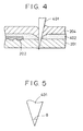
- Figs. 1(a) and 1(b) are schematic illustrations of a process for manufacturing an optical recording medium in accordance with the present invention.
- Fig. 1(a) is a schematic plan view of an optical card of a work size; and
- Fig. 1(b) is a schematic sectional view of the optical card taken along the line A-A of Fig. 1(a).
- reference numeral 101 denotes a work sized optical card
- reference numeral 102 denotes a broken line indicating a predetermined size of the optical card
- reference numeral 103 denotes an area of the optical card, in which information is recorded or information has been recorded.
- reference numeral 104 denotes a substrate of a work size
- reference numeral 105 denotes a protective substrate of a work size
- reference numeral 106 denotes a track groove, formed on the surface of the substrate, nearly parallel to one side along the length of the optical card of a predetermined size
- reference numeral 107 denotes a recording layer
- reference numeral 108 denotes an adhesive layer.
- a cutting edge 109 is brought into contact with a position 102 of the predetermined size of the optical card 101, and is made to enter along the thickness of the optical card in order to cut out an optical card of a predetermined size from a work sized optical card.
- a cutting edge 109 is brought into contact with a position 102 of the predetermined size of the optical card 101, and is made to enter along the thickness of the optical card in order to cut out an optical card of a predetermined size from a work sized optical card.
- cutting the adhesive layer 108 at least inside the position 102 (hereinafter abbreviated as a cutting position) where the cutting edge 109 is made to enter the work sized optical card without causing the adhesive layer to be compressed or deformed as the cutting edge enters the optical card is a preferable process because a squeeze out of the adhesive layer from the end surface of the optical card can be effectively prevented.
- the "inside” in the present invention means the recording area side of the optical card from the cutting position.
- the work sized optical card be cut without causing the adhesive layer 108, positioned at inside and outside from the cutting position of the work sized optical card to be substantially deformed, because the adhesive layer 108 can be prevented from squeezing out from the end surface of the rpredetermined ecording medium more completely and cutting accuracy can be further improved.
- an example of a means for preventing the compression and deformation of the adhesive layer 108 is a method in which solid particles 110 are contained in the adhesive layer 108, as shown in Fig. 1(b).
- Solid particles formed of: ceramics such as SiO2, SiO, SiNx, or Al2O; metals such as iron, copper, nickel, or silver; and acrylic resins such as polystyrene, polypropylene, or polymethyl methacrylate may be appropriately selected and used.
- the particle size of these solid particles is from 0.1 to 100 ⁇ m, preferably from 0.5 to 50 ⁇ m, and more preferably from 30 to 50 ⁇ m, though the size depends upon the thickness of the adhesive layer 108, in order to effectively prevent the compression and deformation of the adhesive layer during cutting.
- the content of these solid particles within the adhesive layer is not particularly limited if the deformation of the adhesive layer can be prevented in the cutting step, however, a preferable range thereof is from 20 to 70% by volume and, particularly, from 40 to 60% because the bonding force of the adhesive layer 108 is not decreased.
- a preferable range thereof is from 20 to 70% by volume and, particularly, from 40 to 60% because the bonding force of the adhesive layer 108 is not decreased.
- the solid particles capable of preventing the adhesive layer 108 from being deformed in the above range of the volume percentage within the adhesive layer include: metals having an average particle size of 30 to 50 ⁇ m, ceramics having an average particle size of 40 to 50 ⁇ m, and so on.
- Examples of the adhesive agent used for the adhesive layer 108 include: conventional adhesive agents, for example, thermoplastic adhesive agents, such as polymers and copolymers of vinyl monomers such as vinyl acetate, acrylic ester, methacrylate ester, vinyl chloride, ethylene, acrylic acid, methacrylic acid, or acrylamide, polyamide, polyester, or epoxy; adhesive agents, such as amino resin (urea resin, melamine resin), phenol resin, epoxy resin, urethane resin, or thermoplastic vinyl resin; and rubber-based adhesive agents such as natural rubber, nitrile rubber, chloro rubber, or silicon rubber.
- thermoplastic adhesive agents such as polymers and copolymers of vinyl monomers such as vinyl acetate, acrylic ester, methacrylate ester, vinyl chloride, ethylene, acrylic acid, methacrylic acid, or acrylamide, polyamide, polyester, or epoxy
- adhesive agents such as amino resin (urea resin, melamine resin), phenol resin, epoxy resin, urethane resin, or thermoplastic vinyl resin
- thermoplastic adhesive agent such that the adhesive layer is likely to squeeze out is used during cutting although the recording sensitivity of the recording layer is not particularly deteriorated.
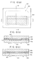
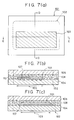
- an adhesive layer 601 having no solid particles is arranged on the recording layer 107 in the recording area 103 as shown in Fig. 6, or an intermediate layer 701 is provided in such a way that the adhesive layer 108 containing solid particles does not directly contact the recording layer 107 in the recording area 103, as shown in Fig. 7 is preferable. This makes it possible to record signals uniformly in the recording area.
- the adhesive agents described above may be used as materials for the adhesive layer 601 and the intermediate layer 701.
- such a work sized optical card can be manufactured by applying an adhesive agent which does not contain solid particles in a portion corresponding to the recording area on a recording film formed on a work sized substrate or laminating an adhesive resin sheet which does not contain solid particles, and applying an adhesive agent which contains solid particles or laminating an adhesive resin sheet in which solid particles are dispersed in outside area of the recording area including the outside area of the cutting position, then laminating a protective substrate, and heating and/or pressurizing them.
- the cutting edge 109 used in the present invention is not limited to that described above.
- a cutting edge made of high speed steel or the like may be used.
- a so-called double-edged cutting edge whose cross section is shaped as shown in Fig. 8(a), or a single-edged cutting edge whose cross section is shaped as shown in Fig. 8(b) may be used. If the angle ⁇ of the cutting edge is set at 10 to 40° and more particularly 15 to 30°, the end surface of the cut optical recording medium can be cut nearly at right angles to the horizontal surface. Therefore, it is possible to obtain an recording medium having good appearance and improve the accuracy of recording/reproduction in the case of the optical card.
- the speed at which the cutting edge enters into the optical recording medium should preferably be set at 2 to 50 mm/sec and, more particularly, 5 to 30 mm/sec, in order to prevent the adhesive layer 108 from squeezing out. Further, cutting while this speed is maintained at a constant speed and/or heating the vicinity of the cutting position prior to the cutting of the optical recording medium is preferable to prevent the substrate and/or the protective substrate from cracking and breaking.
- the temperature in the cut portion is set at 80 to 110°C and, more particularly, 90 to 100°C as the temperature degree though this temperature depends upon materials of the substrate and the protective substrate, and the heating time is set at 30 to 180 sec. and, more particularly, 60 to 120 sec.
- the heating time is set at 30 to 180 sec. and, more particularly, 60 to 120 sec.
- one cycle is terminated when, after the cutting edge is made to enter the optical recording medium along the full thickness thereof as shown in Fig. 9(a), the cutting edge is pulled out from the optical recording medium, however, in the present invention, it is preferable that the cutting edge enter the optical recording medium along the full thickness thereof is moved outwardly as shown in Fig. 9(b) so that the cutting edge does not contact the end surface of the cut optical recording medium, because it is possible to prevent the members from being separated in the end portion of the optical recording medium.
- the present invention is not limited to such a structure.
- it may also be preferably used in an optical recording medium in which a substrate and a protective substrate are bonded to each other with an adhesive layer 1001 and a spacer 1002 provided in between in an area outside the recording area, as shown in Fig. 10.
- low-melting point metallic materials include: Te, Te-Cu, TeO, Cu-Sn, and Cu-N
- organic dye materials include: polymethine, pyrylium, cyanine, naphthoquinone, and triphenylmethane.
- film formation method there is no need to limit the film formation method, and a conventional process may be used.
- a vacuum film formation process such as vapor disposition or sputtering, may be used for low-melting point metallic materials.
- a gravure printing method or a spin coating method may be used for organic dye materials.
- the substrate 104 and the protective substrate 105 should preferably have a small amount of drawbacks during optical recording and reproduction.
- materials having good moldability are preferable. Examples of preferred materials are: acrylic resin, polycarbonate resin, polyester resin, vinyl resin, polyimide resin, polyacetal resin, polyolefine resin, polyamide resin, and cellulose derivatives.
- An optical card having predetermined size of 85 mm and 54 mm was manufactured by a method described below. Initially, an acrylic resin substrate having a work size (90 mm x 100 mm x 0.4 mm thick) was prepared. Stripe-shaped track grooves having a length of 80 mm, a width of 3 ⁇ m, a pitch of 12 ⁇ m, and a depth of 2,700 to 3,000 ⁇ are held within the area of 30 mm long and 80 mm wide on the surface of the substrate.
- an organic coloring matter solution is applied by a gravure coating method in an area of the surface of the substrate where the track grooves are formed and dried to form a recording layer having a thickness of 1,000 ⁇ 100 ⁇ .
- the work sized optical card was cut into the predetermined secondd card so as to include an area formed a recording layer by using a cutting machine (product name: single puncher CPS type: manufactured by Aisel Co., Ltd.).
- a cutting edge which can cut out the predetermined sized optical card from the work sized optical card indicated as reference numeral 1101 in the perspective view of Fig. 11, was used as the cutting edge 109 of the cutting machine.
- a single-edged cutting edge whose cross section inside the cutting position is at right angles to the horizontal surface as shown in Fig. 8(b) was used.
- the angle ⁇ was set at 20°.
- the speed of the cutting edge at which it enters the optical card was set at 15 mm/sec.
- the thickness of the adhesive layer after cutting was not 85% or less that of the adhesive layer before cutting in the end surface of the adhesive layer, and thus the adhesive layer was not substantially deformed.
- the squeeze out of the adhesive layer in the end surface of the optical card thus obtained was evaluated by visual check and touching.
- the presence and absence of the air layer in the interface, an extent that the air layer enters from the end surface into the inside, and the ratio of the end surface where peeling has occurred to the entire circumference of the card were evaluated as regards the peeled state of the substrate and the protective substrate in the end surface of the optical card. The evaluation was performed on the basis of the criteria described below.
- An optical card was manufactured in the same way as in Example 1 except that glass beads were not contained in the adhesive layer.
- the adhesive layer was cut in the same manner as in Example 1, the thickness of the adhesive layer after cutting was 65% of the original thickness.
- the squeeze out and peeled state of the adhesive layer of the optical card thus obtained were evaluated. The results of the evaluation are shown in Table 1.
- An optical card of a work size was manufactured in the same way as in Example 1. Thereafter, the cutting position was heated at 80°C for two minutes prior to cutting, after which the optical card was cut in the same manner as in Example 1, thus manufacturing an optical card. No substantial deformation of the adhesive layer occurred.
- the thickness of the adhesive layer of the optical card after cutting was 60% of the thickness before cutting, and a deformation occurred in the adhesive layer.
- a work sized optical card was manufactured in the same way as in Example 1 except that 40% by volume of Al2O3 particles having an average particle size of 40 ⁇ m were contained in place of glass beads.
- An optical card was cut by using a cutting machine used in Example 1 under the condition where the speed at which the cutting edge enters was set at 25 mm/sec, thus manufacturing an optical card. No substantial deformation occurred in the adhesive layer.
- the squeeze out of the adhesive layer was evaluated as "A” for all the cards.
- the peeled state of the cards was evaluated as "A” for all the cards, but as "B” for 10 cards. However, the end surfaces of 5 optical cards were cracked and broken.
- One hundred optical cards were manufactured in the same way as in Example 3 except that the cutting position was heated at 90°C for one minutes before the work sized optical card was cut.
- the adhesive layer was not substantially deformed.
- One hundred optical cards were manufactured in the same way as in Example 4 except that the work sized optical card was cut by using a cutting apparatus shown in Fig. 9.
- An optical card was manufactured in the same way as in Example 1 except that a bisphenol A type polycarbonate resin (product name: Panlite L-1250, manufactured by Teijin Chemicals Ltd.) was used as the work sized substrate and the protective substrate.
- a bisphenol A type polycarbonate resin product name: Panlite L-1250, manufactured by Teijin Chemicals Ltd.
Applications Claiming Priority (2)
| Application Number | Priority Date | Filing Date | Title |
|---|---|---|---|
| JP15810893 | 1993-06-04 | ||
| JP158108/93 | 1993-06-04 |
Publications (1)
| Publication Number | Publication Date |
|---|---|
| EP0627734A1 true EP0627734A1 (de) | 1994-12-07 |
Family
ID=15664482
Family Applications (1)
| Application Number | Title | Priority Date | Filing Date |
|---|---|---|---|
| EP19940303670 Withdrawn EP0627734A1 (de) | 1993-06-04 | 1994-05-23 | Verfahren zur Herstellung eines optischen Aufzeichnungsmediums |
Country Status (2)
| Country | Link |
|---|---|
| US (1) | US5806388A (de) |
| EP (1) | EP0627734A1 (de) |
Cited By (2)
| Publication number | Priority date | Publication date | Assignee | Title |
|---|---|---|---|---|
| FR2809857A1 (fr) * | 2000-06-06 | 2001-12-07 | Yves Sennegon | Procede de realisation d'un disque compact de type cd-rom de dimensions reduites |
| EP1296319A1 (de) * | 2000-04-25 | 2003-03-26 | Matsushita Electric Industrial Co., Ltd. | Verfahren zur herstellung eines plattensubstrats und verfahren und vorrichtung zur herstellung einer optischen platte |
Families Citing this family (10)
| Publication number | Priority date | Publication date | Assignee | Title |
|---|---|---|---|---|
| US20040027981A1 (en) * | 2000-10-24 | 2004-02-12 | Schoeppel Wolfgang G | Optical storage medium |
| EP1202265A1 (de) * | 2000-10-24 | 2002-05-02 | 3M Innovative Properties Company | Optisches Aufzeichnungsmedium und System zu seiner Herstellung |
| US20040042379A1 (en) * | 2000-10-24 | 2004-03-04 | Schoeppel Wolfgang G | Optical storage medium |
| TWI242206B (en) * | 2001-06-22 | 2005-10-21 | Fuji Photo Film Co Ltd | Optical information recording medium |
| US7341820B2 (en) * | 2001-11-30 | 2008-03-11 | Fujifilm Corporation | Optical information recording medium |
| US6820784B2 (en) * | 2001-12-21 | 2004-11-23 | Eastman Kodak Company | Method of cutting a laminated web and reducing delamination |
| EP1843337B1 (de) * | 2002-01-23 | 2009-03-25 | FUJIFILM Corporation | Optisches Informationsaufzeichnungsmedium |
| CN100341059C (zh) * | 2002-12-19 | 2007-10-03 | 富士胶片株式会社 | 光信息记录方法及光信息记录介质 |
| AU2003303243A1 (en) * | 2002-12-19 | 2004-07-14 | Omd Productions Ag In Liquidation | Data carrier |
| US11275460B2 (en) * | 2019-04-26 | 2022-03-15 | Samsung Display Co., Ltd. | Display device |
Citations (6)
| Publication number | Priority date | Publication date | Assignee | Title |
|---|---|---|---|---|
| EP0251794A2 (de) * | 1986-07-01 | 1988-01-07 | Kyodo Printing Co., Ltd. | Herstellungsmethode für eine optische Aufzeichnungskarte |
| JPH0210537A (ja) * | 1988-06-29 | 1990-01-16 | Canon Inc | 情報記録媒体の製造方法 |
| JPH0231344A (ja) * | 1988-07-20 | 1990-02-01 | Canon Inc | 情報記録媒体およびその製造方法 |
| JPH03185642A (ja) * | 1989-12-14 | 1991-08-13 | Canon Inc | 情報記録媒体の切断方法 |
| US5077725A (en) * | 1988-07-08 | 1991-12-31 | Sharp Kabushiki Kaisha | Optical memory device and apparatus for manufacturing the same |
| EP0494479A1 (de) * | 1989-02-27 | 1992-07-15 | Del Mar Avionics | Auf Glas basierende optische Platte und deren Herstellungsverfahren |
Family Cites Families (13)
| Publication number | Priority date | Publication date | Assignee | Title |
|---|---|---|---|---|
| JPS6150236A (ja) * | 1984-08-18 | 1986-03-12 | Canon Inc | 磁気記録媒体の製造方法 |
| US4606250A (en) * | 1985-07-25 | 1986-08-19 | Eumuco Aktiengesellschaft Fur Maschinenbau | Apparatus for producing blanks from a web |
| JPS6288154A (ja) * | 1985-10-14 | 1987-04-22 | Daicel Chem Ind Ltd | 光デイスクの製造方法 |
| JP2585520B2 (ja) * | 1985-12-27 | 1997-02-26 | 株式会社日立製作所 | 相変化記録媒体 |
| US5026623A (en) * | 1986-04-21 | 1991-06-25 | Canon Kabushiki Kaisha | Optical recording medium |
| US5249176A (en) * | 1987-07-20 | 1993-09-28 | Canon Kabushiki Kaisha | Optical recording medium, process for preparing the same and its optical recording and reproducing system |
| US5085925A (en) * | 1987-08-12 | 1992-02-04 | Canon Kabushiki Kaisha | Optical recording medium |
| US5344304A (en) * | 1987-09-05 | 1994-09-06 | Canon Kabushiki Kaisha | Mold for molding of substrate for information recording medium |
| US5174937A (en) * | 1987-09-05 | 1992-12-29 | Canon Kabushiki Kaisha | Method for molding of substrate for information recording medium and method for preparing substrate for information recording medium |
| US5075060A (en) * | 1988-11-16 | 1991-12-24 | Canon Kabushiki Kaisha | Process for producing a substrate sheet for an optical recording medium |
| EP0376678B1 (de) * | 1988-12-28 | 1995-03-01 | Canon Kabushiki Kaisha | Informationsaufzeichnungsträger |
| US4964934A (en) * | 1989-02-02 | 1990-10-23 | Del Mar Avionics | Optical disk manufacturing process |
| US5058925A (en) * | 1989-12-13 | 1991-10-22 | The Standard Register Company | Leach resistant ink for protecting documents from alteration and document protected thereby |
-
1994
- 1994-05-23 EP EP19940303670 patent/EP0627734A1/de not_active Withdrawn
-
1997
- 1997-02-04 US US08/795,727 patent/US5806388A/en not_active Expired - Fee Related
Patent Citations (6)
| Publication number | Priority date | Publication date | Assignee | Title |
|---|---|---|---|---|
| EP0251794A2 (de) * | 1986-07-01 | 1988-01-07 | Kyodo Printing Co., Ltd. | Herstellungsmethode für eine optische Aufzeichnungskarte |
| JPH0210537A (ja) * | 1988-06-29 | 1990-01-16 | Canon Inc | 情報記録媒体の製造方法 |
| US5077725A (en) * | 1988-07-08 | 1991-12-31 | Sharp Kabushiki Kaisha | Optical memory device and apparatus for manufacturing the same |
| JPH0231344A (ja) * | 1988-07-20 | 1990-02-01 | Canon Inc | 情報記録媒体およびその製造方法 |
| EP0494479A1 (de) * | 1989-02-27 | 1992-07-15 | Del Mar Avionics | Auf Glas basierende optische Platte und deren Herstellungsverfahren |
| JPH03185642A (ja) * | 1989-12-14 | 1991-08-13 | Canon Inc | 情報記録媒体の切断方法 |
Non-Patent Citations (3)
| Title |
|---|
| PATENT ABSTRACTS OF JAPAN vol. 14, no. 150 (P - 1025) 22 March 1990 (1990-03-22) * |
| PATENT ABSTRACTS OF JAPAN vol. 14, no. 185 (P - 1036) 13 April 1990 (1990-04-13) * |
| PATENT ABSTRACTS OF JAPAN vol. 15, no. 446 (P - 1274) 13 November 1991 (1991-11-13) * |
Cited By (4)
| Publication number | Priority date | Publication date | Assignee | Title |
|---|---|---|---|---|
| EP1296319A1 (de) * | 2000-04-25 | 2003-03-26 | Matsushita Electric Industrial Co., Ltd. | Verfahren zur herstellung eines plattensubstrats und verfahren und vorrichtung zur herstellung einer optischen platte |
| EP1296319A4 (de) * | 2000-04-25 | 2005-04-13 | Matsushita Electric Ind Co Ltd | Verfahren zur herstellung eines plattensubstrats und verfahren und vorrichtung zur herstellung einer optischen platte |
| US7101593B2 (en) | 2000-04-25 | 2006-09-05 | Matsushita Electric Industrial Co., Ltd. | Method for producing a disk-shaped substrate and method for producing an optical disk |
| FR2809857A1 (fr) * | 2000-06-06 | 2001-12-07 | Yves Sennegon | Procede de realisation d'un disque compact de type cd-rom de dimensions reduites |
Also Published As
| Publication number | Publication date |
|---|---|
| US5806388A (en) | 1998-09-15 |
Similar Documents
| Publication | Publication Date | Title |
|---|---|---|
| EP0627734A1 (de) | Verfahren zur Herstellung eines optischen Aufzeichnungsmediums | |
| EP0375298B1 (de) | Medium für optische Datenspeicherung | |
| EP0280531B1 (de) | Optischer Datenaufzeichnungsträger | |
| EP0317696B1 (de) | Medium für optische Datenaufzeichnung | |
| US7962927B2 (en) | Optical disk | |
| US5328816A (en) | Process for producing optical recording medium | |
| EP0680039B1 (de) | Informationsaufzeichnungsträger und Verfahren zu seiner Herstellung | |
| US4543307A (en) | Optical data storage and recording media having recording surface protection | |
| JPH0553021B2 (de) | ||
| EP0259151B1 (de) | Optische Karte und Verfahren zu ihrer Herstellung | |
| JPH058116B2 (de) | ||
| JP2687564B2 (ja) | 光カード | |
| JPH0750036A (ja) | 光記録媒体の製造方法 | |
| US6527904B1 (en) | Method of producing an optical video disc | |
| JP2715176B2 (ja) | 光記録媒体 | |
| JPS6126931A (ja) | 転写用磁気テ−プ | |
| JPH02185734A (ja) | 光記録媒体およびその製造方法 | |
| JP2510803B2 (ja) | 光記録媒体 | |
| JPH0744896A (ja) | カード型情報記録媒体端面部の熱処理加工方法 | |
| JPH07302439A (ja) | 情報用光ディスク及びその製造方法 | |
| JPH04109442A (ja) | 情報記録媒体の製造方法 | |
| JPH11154214A (ja) | Icモジュール付き光カード | |
| JPH0344837A (ja) | 光カード | |
| JPH09138844A (ja) | 光カード | |
| JP2000242974A (ja) | 貼り合せ型ディスク基板およびその製造方法 |
Legal Events
| Date | Code | Title | Description |
|---|---|---|---|
| PUAI | Public reference made under article 153(3) epc to a published international application that has entered the european phase |
Free format text: ORIGINAL CODE: 0009012 |
|
| AK | Designated contracting states |
Kind code of ref document: A1 Designated state(s): DE FR GB IT NL |
|
| 17P | Request for examination filed |
Effective date: 19950421 |
|
| 17Q | First examination report despatched |
Effective date: 19971022 |
|
| STAA | Information on the status of an ep patent application or granted ep patent |
Free format text: STATUS: THE APPLICATION IS DEEMED TO BE WITHDRAWN |
|
| 18D | Application deemed to be withdrawn |
Effective date: 19980505 |