EP0626794A2 - Appareil et méthode d'interpolation pour améliorer l'ajustement du recouvrement dans un système de télevision par projection - Google Patents
Appareil et méthode d'interpolation pour améliorer l'ajustement du recouvrement dans un système de télevision par projection Download PDFInfo
- Publication number
- EP0626794A2 EP0626794A2 EP94303684A EP94303684A EP0626794A2 EP 0626794 A2 EP0626794 A2 EP 0626794A2 EP 94303684 A EP94303684 A EP 94303684A EP 94303684 A EP94303684 A EP 94303684A EP 0626794 A2 EP0626794 A2 EP 0626794A2
- Authority
- EP
- European Patent Office
- Prior art keywords
- data
- interpolation
- interpolating
- order
- points
- Prior art date
- Legal status (The legal status is an assumption and is not a legal conclusion. Google has not performed a legal analysis and makes no representation as to the accuracy of the status listed.)
- Granted
Links
Images


Classifications
-
- H—ELECTRICITY
- H04—ELECTRIC COMMUNICATION TECHNIQUE
- H04N—PICTORIAL COMMUNICATION, e.g. TELEVISION
- H04N5/00—Details of television systems
- H04N5/74—Projection arrangements for image reproduction, e.g. using eidophor
-
- H—ELECTRICITY
- H04—ELECTRIC COMMUNICATION TECHNIQUE
- H04N—PICTORIAL COMMUNICATION, e.g. TELEVISION
- H04N9/00—Details of colour television systems
- H04N9/12—Picture reproducers
- H04N9/16—Picture reproducers using cathode ray tubes
- H04N9/28—Arrangements for convergence or focusing
-
- H—ELECTRICITY
- H04—ELECTRIC COMMUNICATION TECHNIQUE
- H04N—PICTORIAL COMMUNICATION, e.g. TELEVISION
- H04N3/00—Scanning details of television systems; Combination thereof with generation of supply voltages
- H04N3/10—Scanning details of television systems; Combination thereof with generation of supply voltages by means not exclusively optical-mechanical
- H04N3/16—Scanning details of television systems; Combination thereof with generation of supply voltages by means not exclusively optical-mechanical by deflecting electron beam in cathode-ray tube, e.g. scanning corrections
- H04N3/22—Circuits for controlling dimensions, shape or centering of picture on screen
- H04N3/23—Distortion correction, e.g. for pincushion distortion correction, S-correction
- H04N3/233—Distortion correction, e.g. for pincushion distortion correction, S-correction using active elements
- H04N3/2335—Distortion correction, e.g. for pincushion distortion correction, S-correction using active elements with calculating means
Definitions
- the present invention generally relates to a method and apparatus for performing a registration adjustment for correcting picture distortion and colour shifts occurring in a projection television and, more particularly, to an interpolation method for improving the registration adjustment process.
- Figs. 5A and 5B of the accompanying drawings schematically show a structure of this sort of projection television 1, in which SC indicates a screen on which a picture or image is projected.
- Individual light projecting units that project each of a red component (R), a green component (G), and a blue component (B) of the primary colour picture are provided on the rear side of this screen SC, which constitutes a so-called rear projection television combined with a screen.
- the light projecting unit includes cathode ray tubes (CRTs) for producing the respective primary picture light, deflection yokes DY for deflecting electron beams of these CRTs, and focusing lenses CD for focusing the primary colour picture light formed by the CRTs onto the screen SC.
- CRTs cathode ray tubes
- deflection yokes DY for deflecting electron beams of these CRTs
- focusing lenses CD for focusing the primary colour picture light formed by the CRTs onto the screen SC.
- the respective primary colour picture light irradiated from the light projecting unit is projected via a rear-mounted reflection mirror to the screen SC.
- the screen can be a lenticular screen constructed as a Fresnel lens, for example. It should be noted that when the reflection mirror M is not employed, such as in the structure shown in Fig. 6, the respective primary colour picture light is directly projected from the rear side of the screen SC.
- an optical system is so constructed in the rear projection television 1 with such a structure that the picture light is obliquely projected to the screen SC.
- the optical system since the optical system is asymmetrically arranged with respect to the screen in the rear projection television 1, the picture light projected from the CRTs must be previously distorted in such a manner that the distortion components caused by this asymmetrical arrangement are cancelled in order to project proper pictures without distortion.
- a circuit for performing this registration correction is employed in the rear projection television 1 having the above-described structure, and the structure of the rear projection television 1 will now be explained with reference to Fig. 7 in which a video signal processing circuit 2 separates a video signal inputted from a video signal input terminal Vin into R, G, B signals.
- Video output circuits 3-1, 3-2, 3-3 supply the red component (R), green component (G), blue component (B) of the respective primary colour pictures to the red CRT, green CRT, and blue CRT, respectively.
- a sync separating circuit 4 extracts a horizontal synchronization signal H and a vertical synchronization signal V from the video signal and outputs these sync signals.
- a horizontal oscillating circuit 5 produces a horizontal oscillating signal in response to the horizontal sync signal H from the sync separating circuit 4 and a vertical oscillating circuit 6 produces a vertical oscillating signal in response to the vertical sync signal V from the sync separating circuit 4.
- a horizontal deflection output circuit 7 produces a horizontal deflection signal in accordance with the horizontal oscillating signal and supplies the horizontal deflection signal to the horizontal deflection yoke of the respective CRTs.
- a vertical deflection output circuit 8 produces a vertical deflection signal in accordance with the vertical oscillating signal and supplies the vertical deflection signal to the vertical deflection yokes of the respective CRTs.
- a high-voltage output circuit 9 produces a high voltage based upon the horizontal oscillation signal and applies this high voltage to the anode electrodes of the respective CRTs.
- a registration correction waveform generating circuit 10 generates a registration correction waveform in accordance with the horizontal deflection signal and the vertical deflection signal, by which asymmetry of the projection optical system is eliminated.
- This correction waveform corresponds to a signal waveform for defining picture or image distortion.
- a registration output circuit 11 supplies the correction waveform to a sub-deflection yoke DY1 of each of the three CRTs.
- the sub-deflection yoke DY1 distorts the picture light projected onto the screen SC in response to the correction waveform, so as to cancel the asymmetry of the optical system, thereby forming a proper image without any distortion on the screen SC.
- one approach to improving image registration in a projection television is to generate a correction waveform according to some non-linear function that can alter the deflection of the beam in the cathode ray tube, so that such altered beam when combined with the image distortion caused by the arrangement of the respective tubes relative to the screen will result in a corrected image.
- This approach is seen as an analog approach to providing image registration correction.
- Interpolation is one method to arrive at the correction waveform and it known that interpolation can become complicated and time consuming, especially higher order interpolation. Similarly, digital calculations of the correction waveform are limited in their accuracy by the bit size of the data word used in the calculations.
- an object of the present invention to provide a method and apparatus for registration correction in a projection television system that can reduce or eliminate the drawbacks inherent in the prior art.
- the present invention has been made in an attempt to solve the above-described drawbacks and has an object to provide a data interpolating method and a data interpolating apparatus with short processing time required to execute an interpolation calculation, and also to eliminate the requirement for a non-volatile memory having a large memory capacity.
- a data interpolating method comprises a high order interpolation step where a high order interpolating calculation is carried out relative to setting data allocated to each data point, and first interpolation data calculated by said interpolating calculation is interpolated among the respective data points; and a low order interpolation step where second interpolation data calculated by a low order interpolating calculation is interpolated either between said setting data and said first interpolation data, or between two pieces of said first interpolation data.
- a data interpolating apparatus comprises high order interpolating means for performing a high order interpolating calculation relative to setting data allocated to each data point and for interpolating first interpolation data calculated by said interpolating calculation among the respective data points; and low order interpolating means for interpolating second interpolation data calculated by a low order interpolating calculation between either said setting data and said first interpolation data, or two pieces of said first interpolation data.
- a data interpolating apparatus comprises high order interpolating means for performing a high order interpolating calculation relative to setting data allocated to each data point, and for interpolating first interpolation data calculated by said interpolating calculation among the respective data points; low order interpolating means for interpolating second interpolation data calculated by a low order interpolating calculation between either said setting data and said first interpolation data, or two pieces of said first interpolation data; and converting means for sequentially sampling the setting data corresponding to the respective data points, and said first and second interpolation data interpolated among said data points, and for converting the sampled data into a waveform signal.
- the high order interpolating means causes said setting data corresponding to the respective data points and said first interpolation data interpolated among said data points to be temporarily stored into storage means.
- the above-described high order interpolating means and the low order interpolating means include storage means, respectively, each of which temporarily stores the setting data corresponding to the respective data points, and said first and second interpolation data interpolated among said data points.
- the present invention provides a system wherein a bit number of registration adjusting data for 3 primary colour picture signals is "n", m-bit data is added to data smaller than LSB of said data having the bit number of "n”, which will then be converted into (n+m)-bit data.
- An interpolation is carried out with the value of said (n+m)-bit data, thereby outputting (n+m)-bit interpolation data, and said interpolation data is converted via a D/A converter into an analog signal which will then constitute deflection correction data for each projection tube.
- a colour image appliance is constructed of a registration correction waveform generating unit for employing such a registration interpolating method.
- the high order interpolation calculation is performed relative to the setting data allocated to the respective data points at the high order interpolation step, and the first interpolation data calculated by this interpolating calculation is interpolated among the respective data points.
- the interpolation is calculated between either the setting data and the first interpolation data, or two pieces of the first interpolation data based on the second interpolation data calculated by the low order interpolating calculation.
- the high order interpolation calculation is performed to the setting data allocated to the respective data points at the high order interpolation step, and the first interpolation data calculated by this interpolating calculation is interpolated among the respective data points.
- the interpolation is calculated between either the setting data and the first interpolation data, or two pieces of the first interpolation data based on the second interpolation data calculated by the low order interpolating calculation.
- the capacity of the non-volatile memory for setting the adjustment points can be reduced, and the system may be realized with employment of a low-cost non-volatile memory.
- the interpolation errors may be set within the allowable range and the adjustment time required to input the setting data may be shortened.
- Fig. 1 is a block diagram of an arrangement of a registration correction waveform generating circuit 10 according to one embodiment of the present invention.
- Other similar embodiments are shown in Figs. 8 and 10 and the same reference numerals shown in the related units of Fig. 8 and Fig. 10 are employed as those for indicating the same or similar components, and explanations thereof are omitted.
- Fig. 8 first, one arrangement of the above-described registration correction wave generating circuit will be explained, in which a CPU 10a controls various portions of the circuit.
- the CPU 10a produces registration setting data and interpolates this setting data to calculate the interpolation data.
- An electrically writable and erasable non-volatile memory (EEPROM) 10b is provided in which the registration setting data output from the CPU 10a is written in response to an address signal supplied from a timing generator 10d.
- This timing generator 10d generates address signals corresponding to the horizontal sync signal H and the vertical sync signal V.
- a static RAM 10C is provided into which the setting data and the interpolation data are written in response to the above-described address signal. That is to say, the CPU 10a performs the high order, more than second order, interpolation calculation relative to the registration setting data read out from the EEPROM 10b, whereby both the calculated interpolation data and the above-described setting data are sequentially written into the static RAM 10c in response to the address signals corresponding to the horizontal sync signal H and the vertical sync signal V.
- a D/A converter 10e converts the setting data and the interpolation data read out from the static RAM 10c under control of the CPU 10a into the respective registration correction waveform signals to be outputted.
- the registration correction waveform generating circuit 10 with such an arrangement generates correction waveforms for the red component (R), green component (G), and blue component of the respective primary colour pictures, and supplies the correction waveforms to the sub-deflection yokes DY1 arranged for the respective colour components.
- the generating circuit 10 with the first arrangement generates the correction waveforms based upon the operations shown in Fig. 9.
- the process operation by the CPU 10a is advanced to a step Sal at which an initial registration adjustment is executed.
- This initial registration adjustment corresponds to such an adjustment that picture light projected from the respective CRTs onto the screen is displayed with substantially proper conditions.
- the CPU 10a writes the setting data produced in correspondence with this adjusting operation into the EEPROM 10b.
- steps Sa2 to Sa4 represent operation for such a case that the rear projection television displays the normal image after the above-described initial registration adjustment.
- the CPU 10a reads the setting data obtained by the above-described initial registration adjustment from the EEPROM 10b, and then the process operation is advanced to the next step Sa3.
- the read setting data are interpolated based on the more than second order function, thereby producing the interpolation data.
- This interpolation data is produced in such a manner that, as represented in Fig.
- the setting data which are indicated by white dots in this figure are allocated on the horizontal scanning line in each of preselected dot intervals, and the registration correcting amounts corresponding to the respective display dots among these setting data are obtained by way of the interpolation calculation.
- the interpolation data obtained by the interpolation calculation are written into the static RAM 10c together with the setting data, and the process operation is advanced to the next step Sa4.
- the setting data and the interpolation data are successively read from the RAM 10c in accordance with the address signals corresponding to the horizontal sync signal H and the vertical sync signal V.
- These data are supplied to the D/A converter 10e, thereby being converted into analog signals which will then be supplied as the registration correction waveforms to the sub-deflection yokes DY1.
- correct pictures from which picture distortion caused by asymmetry of the optical system has been eliminated are projected onto the screen SC.
- Fig. 12A represents the display screen and indicates a relationship between the setting data for forming the display dots and the interpolation data.
- the white dot corresponds to a display dot to which the setting data has been allocated
- the black dot is a display dot indicative of the interpolation data interpolated in accordance with the white dots.
- the white dots constituting the setting data are set for every 8 dots along both the horizontal and vertical directions, and the interpolation data or interpolation levels are calculated at the black dot positions by the interpolation calculation based on the more than second order function with the employment of at least more than three setting data.
- the white dots (1,1), (1,9) and (1,17) are employed as the setting data, and the more than second order interpolation calculation is carried out, so that the interpolation levels in the seven black dots among these white dots are successively interpolated.
- the setting data produced by the initial registration adjustment are written into the EEPROM 10b, the interpolation data obtained from the interpolation calculation during the normal use are written into the RAM 10c together with the setting data, and then picture distortion is corrected in accordance with these data.
- the correction waveforms are produced based upon an operation shown in Fig. 11. That is to say, when the rear projection television is set to the registration adjustment mode, the process operation of the CPU 10a is advanced to a step Sb1 at which the registration adjustment is performed. In this registration adjustment step, while a user observes the screen, the user manipulates a remote controller or a key switch so that the picture light projected from the respective CRTs onto the screen SC is properly displayed. Next, when the process operation is advanced to a step Sb2, the CPU 10a generates the setting data in response to the above-described adjustment operation, and writes the setting data into the EEPROM 10b. Then, the process operation is advanced to the next step Sb3.
- the interpolation calculation is carried out in the condition as shown in Fig. 12, thereby producing the interpolation data. Then, the interpolation data obtained by the interpolation calculation are written into the EEPROM 10b. Subsequently, at a step Sb4, the setting data and the interpolation data are sequentially read out from the EEPROM 10b in response to the address signals corresponding to the horizontal sync signal H and the vertical sync signal V. These data are supplied to the D/A converter 10e, thereby producing the registration correction waveforms which will then be supplied to the sub-deflection yokes DY1. As a consequence, the proper pictures from which the picture distortion caused by asymmetry of the optical system has been removed are projected onto the screen SC.
- a different point of the embodiment shown in Fig. 1 from the second structure shown in Fig. 10 is that a calculating circuit 10f for performing first order, that is, linear, interpolation by means of hardware is employed.
- the calculating circuit 10f reads out either the setting data, or the high order interpolation data stored in the EEPROM 10b, and then interpolates data between the read-out setting data and the high order interpolation data by way of the first order interpolation, thereby producing low order interpolation data.
- the respective setting data are produced during the registration adjustment. While these setting data are interpolated with the interpolation data by way of the interpolation calculation during the picture projection, the correction waveforms are produced based upon the interpolation data and the setting data, whereby distortion of this picture is corrected.
- the load of the CPU 10a becomes large, and a lengthy time period is required to execute the high order interpolation calculation.
- the circuit arrangement becomes complex because the setting data and the interpolation data must be read/written from/into the EEPROM 10b and the RAM 10c, resulting in higher product cost.
- a process operation of a CPU 10a executes a step Scl shown in Fig. 2 to perform an initial registration adjustment.
- the initial registration adjustment implies that, as previously stated, such an adjustment is carried out to substantially properly display picture light projected from the respective CRTs onto the screen SC.
- a remote controller or a key switch is operated by the user, whereby the picture light projected from the respective CRTs to the screen SC can be substantially properly displayed thereon.
- the process operation of the CPU 10a is advanced to a step Sc2. It should be noted, as shown by the white dots of Fig. 3, that this setting data is produced in correspondence with each of the predetermined dot intervals on the respective horizontal scanning line in the display screen. Then, when the process operation is advanced to a step Sc2, the setting data produced in response to the adjustment operation is written into the EEPROM 10b corresponding to the non-volatile memory, and the process operation is advanced to the next step Sc3.
- step Sc3 at least three pieces of setting data are read out from the EEPROM 10b for every horizontal scanning line, and high order interpolation data are produced among these setting data by way of more than second order, that is, high-order interpolation calculations are used to perform the interpolation.
- the high-order interpolation data represents a correction amount of registration at a display dot positioned at a centre between the respective setting data indicated by the white dots.
- the registration correction amounts are obtained based on the setting data, which are the white dots, and the high-order interpolation data, which are the black dots, for every horizontal scanning line.
- step subsequent to step Sc4 represents an operation performed when the rear projection television displays a normal picture.
- the above-described calculation circuit 10f produces the low order interpolation data based on the setting data and the high-order interpolation data.
- the CPU 10a reads both the setting data and the high order interpolation data from the EEPROM 10b in response to the address signals corresponding to the horizontal sync signal H and the vertical sync signal V, and then supplies the setting data and the high order interpolation data to the calculation circuit 10f.
- the calculation circuit 10f interpolates the registration correction amounts at the respective amounts at the respective display dots indicated by the black dots in Fig. 3 by linear interpolation of the data between the setting data and the high order interpolation data, as illustrated in Fig. 4.
- step Sc5 when the process operation is advanced to step Sc5, the setting data and the high order interpolation data, which are read out from the EEPROM 10b in response to the address signals corresponding to the horizontal sync signal H and the vertical sync signal V and, further, the low order interpolation data calculated in accordance with these data are supplied to the D/A converter 10e and converted into analog signals which will then be supplied as the registration correction waveforms to the sub-deflection yokes DY1. As a result, a proper picture without any picture distortion is displayed on the screen SC.
- the setting data are produced in accordance with the initial registration adjustment operation, and furthermore, one piece of high order interpolation data is interpolated among the setting data by way of the interpolation calculation with at least three pieces of setting data employed for every horizontal scanning line. Then, the registration correction amounts of the respective display dots corresponding to the data among the setting data and the high order interpolation data, may be obtained by means of the linear interpolation by using the setting data and the high-order interpolation data.
- the calculating circuit 10f executes the low-order interpolation calculation in the hardware mode, the low-order interpolation can be calculated at a high speed without loading down the CPU 10a.
- non-volatile memory EEPROM 10b having a large memory capacity for storing the setting data and the interpolation data corresponding to the number of display dots for a single picture is required in one of the approached discussed above, this embodiment requires only 1/5 of the memory capacity of the conventional memory. Thus, such a non-volatile memory with a large memory capacity is not required in the above-explained embodiment.
- Fig. 13 is a block diagram of a circuit arrangement of a rear projection television according to an embodiment of the present invention, in which a sync separating circuit 61 separates the horizontal sync signal H and the vertical sync signal V from a video signal input to this sync separating circuit 61.
- the horizontal sync signal H forms a scanning signal in a horizontal oscillating circuit 63, which will then be supplied via a horizontal deflection output circuit 64 to main deflection coils 75R, 75G, and 75B.
- the vertical sync signal V is supplied via a vertical deflection output circuit 67 to the main deflection coils 75R, 75G, 75B mounted on neck portions of a red CRT 65R, a green CRT 65G, and a blue CRT 65B.
- the high voltage is applied from the horizontal oscillating circuit 63 via a high voltage output circuit 68 to an anode electrode of each of the CRTs 65R, 65G, and 65B.
- From the horizontal deflection output circuit 64 and the vertical deflection output circuit 67, data used to produce the correction waveforms corresponding to the interpolation point region of the image are output to a registration correction wave generating unit 69 the details of which will be set forth below.
- the correction data for the respective colours derived from the registration correction wave generating unit 69 are amplified in a registration output unit 70, and then the respective amplified correction data are supplied to the respective sub deflection coils 74R, 74G, 74B arranged near the main deflection coils 75R, 75G, 75B for the respective CRTs 65R, 65G, 65B.
- the video signals processed in the video signal processing circuit 62 with respect to various signal processing operations, are amplified in a video output unit 71 to produce the R, G, B colour drive signals, which are supplied to the cathode electrode terminals of the red CRT 65R, the green CRT 65G, and the blue CRT 65B.
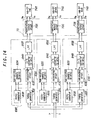
- Fig. 14 is a circuit block diagram showing in more detail the registration correction waveform generating unit 69 for the respective primary colour signals.
- this registration correction waveform generating unit 69 is made up of a red waveform generating unit 69R, a green waveform generating unit 69G, and a blue waveform generating unit 69B.
- the correction waveform data are calculated with respect to the respective CRTs 65R, 65G, 65B in each of the waveform generating units 69R, 69G, 69B, and the calculated correction waveform data are supplied via the registration output circuits 70R, 70G, 70B to the respective sub-deflection coils 74R, 74G, 74B.
- a microcomputer 80R, 80G, 80B is provided for each colour signal and operates to set various sorts of data about the setting data for the adjustment points.
- a timing generator 81R, 81G, 81B for each colour generates a control signal at a predetermined timing based on the horizontal and vertical sync signals fed thereto.
- a non-volatile memory 82R, 82G, 82B for each colour signal sets the setting data about the adjustment points with 8-bit resolution.
- a calculating circuit 83R, 83G, 83B for each of the colour signals performs a calculation process in which 4-bit data is added to 8-bit data relating to the adjustment point.
- the resolution of the added 8-bit data becomes identical to 12-bit resolution of the respective D/A converters 84R, 84G, 84B provided in the following stage.
- a low-pass filter 85R, 85G, 85B for each of the three colour signals smooths the respective outputs of the D/A converters 84T, 84G, 84B.
- the 8-bit adjustment point is set as initial data into the non-volatile, 8-bit memories 82R, 82G, 82B, respectively. Then, this 8-bit data is read out from the non-volatile memories 82R, 82G, 82B, and then 4-bit data is added to this read-out 8-bit data in the calculating circuits 84R, 84G, 84B in such a way that the resultant data has the same data length as the resolution of the D/A converters 85R, 85G, 85B.
- an interpolation calculating process is performed based on 12 bits in the calculating circuits 84R, 84G, 84B in order to calculate the interpolation data for the three colour signals, and the calculated 12-bit interpolation data is outputted to the respective D/A converters 85r, 85G, 85B.
- the 12-bit interpolation data which has been converted from digital to analog in the D/A converters 84R, 84G, 84B is smoothed in the respective low-pass filters 85R, 85G, 85B, and supplied via the respective registration output circuit 70R, 70G, 70B to the respective sub-deflection coil 74R, 74G, 74B.
- Fig. 15 schematically shows the situation in which the 4-bit data is added in each of the calculating circuits 84R, 84G, 84B.
- the data of the adjustment point is set into the non-volatile memory 82 in 8 bits and when the interpolation calculation process is carried out in the calculation processing unit 84, 4-bit additional data, as shown by dotted line circles in Fig. 15, is first added as data smaller than the LSB of the 8-bit adjustment data read out from the non-volatile memories 82Rm 82G, 82B. All of the 4-bit additional data are identical to each other and all have an arbitrary value.
- the adjustment point data to which the additional data has been added is handled as 12-bit data to be interpolated.
- the interpolation calculation process is carried out and the resultant interpolated data is outputted to the respective D/A converters 85R, 85G, 85B.
- the 12-bit interpolation data processed by the interpolation calculation process is digital to analog converted by respective the D/A converters 85R, 85G, 85B.
- Fig. 16 is a flow chart representing a processing operation effected in the registration correction waveform generating unit 69 of Fig. 13.
- registration correction data obtained from such a measuring device as image distortion and convergence is first set as 8-bit data for every adjustment point in step S001, and the setting data is written into the non-volatile memories 82R, 82G, 82B in step S002. Then, when the correction waveforms to be applied to the sub-deflection coils 74R, 74G, 74B for correcting image distortion are generated, the setting data set at 8 bits into the non-volatile memories 82R, 82G, 82B are read out in step S003. In the calculating circuits 83R, 83G, 83B, 4-bit additional data is added to the 8-bit setting data in step S004.
- step S005 the interpolation data calculated at step S005 is digital to analog converted in the D/A converters 85R, 85G, 85B in 12-bit resolution, and the resultant interpolation data is outputted as correction deflection waveform data in step S006.
- Fig. 17 schematically shows one example of interpolation data calculated by the above-described interpolation calculation process.
- the abscissa indicates an interpolation point, and the ordinate axis represents a level of the interpolation point in hexadecimal notation.
- the black circle represents 8-bit setting data of adjustment points, and the white circle denotes 12-bit interpolation data of the interpolation points.
- the setting data 800H and 810H at points A and B are interpolated at sixteen interpolation points, which are outputted as 12-bit data.
- the setting data is selected to be 8 bits, interpolation precision thereof is lowered as compared with that of the conventional 12-bit data, as shown by the white triangle, however, since this 8-bit setting data is converted into the 12-bit analog signal after being interpolated, the correction waveform thereof can be smoothed.
- precision of the lower 4-bit data is within the allowable range with regard to the registration correction.
- Fig. 18 is a block diagram an example of a circuit portion of such a registration correction waveform generating unit 69 shown in Fig. 13.
- a microcomputer 90 for performs various control operations, such as setting of data about adjustment points and writing into the 12-bit non-volatile memory 91.
- a timing generator 92 generates a control signal at a predetermined timing based on the horizontal sync signal H and the vertical sync signal V fed thereto.
- a calculating circuit 43 calculates interpolation data and the like based on the data set into the non-volatile memory 91.
- a 12-bit D/A converter 94, and a low-pass filter 95 for smoothing the output from the 12-bit D/A converter 94 are provided.
- a region of an image is determined by, for example, 8 points in the horizontal direction and 10 points in the vertical direction.
- the data of these adjustment points is set as 12-bit digital data, and the setting data is written into the on-volatile memory 91.
- the setting data about the adjustment points which have been set into the non-volatile memory 91 are read out.
- the calculation process to calculate the interpolation data among the adjustment points is performed in the calculating circuit 93.
- the calculated interpolation data are amplified and filtered via the low-pass filter 95 by the registration output circuit, and the amplified interpolation data are outputted as the deflection waveform data to the sub DY.
Landscapes
- Engineering & Computer Science (AREA)
- Multimedia (AREA)
- Signal Processing (AREA)
- Video Image Reproduction Devices For Color Tv Systems (AREA)
Priority Applications (1)
| Application Number | Priority Date | Filing Date | Title |
|---|---|---|---|
| EP00117606A EP1067803A2 (fr) | 1993-05-27 | 1994-05-23 | Méthode et dispositif d'interpolation pour améliorer l'ajustement de la convergence dans un système de télévision par projection |
Applications Claiming Priority (6)
| Application Number | Priority Date | Filing Date | Title |
|---|---|---|---|
| JP14852093 | 1993-05-27 | ||
| JP5148520A JPH06337894A (ja) | 1993-05-27 | 1993-05-27 | データ補間方法および装置 |
| JP148520/93 | 1993-05-27 | ||
| JP19185293 | 1993-07-07 | ||
| JP19185293A JP3341373B2 (ja) | 1993-07-07 | 1993-07-07 | カラー映像機器とそのレジストレーション補間方式 |
| JP191852/93 | 1993-07-07 |
Related Child Applications (1)
| Application Number | Title | Priority Date | Filing Date |
|---|---|---|---|
| EP00117606A Division EP1067803A2 (fr) | 1993-05-27 | 1994-05-23 | Méthode et dispositif d'interpolation pour améliorer l'ajustement de la convergence dans un système de télévision par projection |
Publications (3)
| Publication Number | Publication Date |
|---|---|
| EP0626794A2 true EP0626794A2 (fr) | 1994-11-30 |
| EP0626794A3 EP0626794A3 (fr) | 1998-04-22 |
| EP0626794B1 EP0626794B1 (fr) | 2003-07-16 |
Family
ID=26478685
Family Applications (2)
| Application Number | Title | Priority Date | Filing Date |
|---|---|---|---|
| EP94303684A Expired - Lifetime EP0626794B1 (fr) | 1993-05-27 | 1994-05-23 | Appareil et méthode d'interpolation pour améliorer l'ajustement du recouvrement dans un système de télevision par projection |
| EP00117606A Withdrawn EP1067803A2 (fr) | 1993-05-27 | 1994-05-23 | Méthode et dispositif d'interpolation pour améliorer l'ajustement de la convergence dans un système de télévision par projection |
Family Applications After (1)
| Application Number | Title | Priority Date | Filing Date |
|---|---|---|---|
| EP00117606A Withdrawn EP1067803A2 (fr) | 1993-05-27 | 1994-05-23 | Méthode et dispositif d'interpolation pour améliorer l'ajustement de la convergence dans un système de télévision par projection |
Country Status (4)
| Country | Link |
|---|---|
| US (1) | US5537159A (fr) |
| EP (2) | EP0626794B1 (fr) |
| KR (2) | KR100307108B1 (fr) |
| DE (1) | DE69432945T2 (fr) |
Cited By (2)
| Publication number | Priority date | Publication date | Assignee | Title |
|---|---|---|---|---|
| EP0746146A2 (fr) * | 1995-05-31 | 1996-12-04 | Sony Corporation | Correction de forme d'ondes de déflection horizontale et verticale |
| DE19611059A1 (de) * | 1996-03-21 | 1997-09-25 | Thomson Brandt Gmbh | Verfahren zur Signalgewinnung in elektronischen Geräten mittels Interpolation zwischen Stützstellenwerten |
Families Citing this family (25)
| Publication number | Priority date | Publication date | Assignee | Title |
|---|---|---|---|---|
| US6969635B2 (en) * | 2000-12-07 | 2005-11-29 | Reflectivity, Inc. | Methods for depositing, releasing and packaging micro-electromechanical devices on wafer substrates |
| US5739870A (en) * | 1996-03-11 | 1998-04-14 | Display Laboratories, Inc. | Math engine for generating font gradients |
| JP3735158B2 (ja) * | 1996-06-06 | 2006-01-18 | オリンパス株式会社 | 画像投影システム、画像処理装置 |
| DE19632188A1 (de) * | 1996-08-09 | 1998-02-12 | Thomson Brandt Gmbh | Verfahren und Vorrichtung zur Gewinnung von Korrekturwerten für Videozeilen eines Videobildes |
| US6437829B1 (en) | 1997-01-16 | 2002-08-20 | Display Laboratories, Inc. | Alignment of cathode ray tube displays using a video graphics controller |
| US6285397B1 (en) | 1997-01-16 | 2001-09-04 | Display Laboratories, Inc. | Alignment of cathode ray tube video displays using a host computer processor |
| US5969486A (en) * | 1997-01-16 | 1999-10-19 | Display Laboratories, Inc. | Detecting horizontal blanking time in cathode ray tube devices |
| KR100226869B1 (ko) * | 1997-03-29 | 1999-10-15 | 구자홍 | 컨버젼스 시스템에서의 수평/수직 보간장치 및 그 제어방법 |
| US6020937A (en) * | 1997-05-12 | 2000-02-01 | Sony Corporation | High resolution digital projection TV with dynamically adjustable resolution utilizing a system of rotating mirrors |
| US6281950B1 (en) | 1997-06-16 | 2001-08-28 | Display Laboratories, Inc. | High speed digital zone control |
| US6067127A (en) * | 1997-07-08 | 2000-05-23 | Sony Corporation | Method and apparatus for reducing the rotation rate of mirrors in a high resolution digital projection display |
| US6091461A (en) * | 1997-08-14 | 2000-07-18 | Sony Corporation | Electronically self-aligning high resolution projection display with rotating mirrors and piezoelectric transducers |
| KR100267729B1 (ko) * | 1998-04-30 | 2000-10-16 | 윤종용 | 영상 신호의 수평 편향 보간 장치 |
| US6962419B2 (en) | 1998-09-24 | 2005-11-08 | Reflectivity, Inc | Micromirror elements, package for the micromirror elements, and projection system therefor |
| US6433840B1 (en) * | 1999-07-22 | 2002-08-13 | Evans & Sutherland Computer Corporation | Method and apparatus for multi-level image alignment |
| US7167297B2 (en) | 2000-08-30 | 2007-01-23 | Reflectivity, Inc | Micromirror array |
| US7023606B2 (en) * | 2001-08-03 | 2006-04-04 | Reflectivity, Inc | Micromirror array for projection TV |
| US7042622B2 (en) * | 2003-10-30 | 2006-05-09 | Reflectivity, Inc | Micromirror and post arrangements on substrates |
| US7437013B2 (en) * | 2003-12-23 | 2008-10-14 | General Instrument Corporation | Directional spatial video noise reduction |
| US7373013B2 (en) * | 2003-12-23 | 2008-05-13 | General Instrument Corporation | Directional video filters for locally adaptive spatial noise reduction |
| CN101617354A (zh) | 2006-12-12 | 2009-12-30 | 埃文斯和萨瑟兰计算机公司 | 用于校准单个调制器投影仪中的rgb光的系统和方法 |
| US8358317B2 (en) | 2008-05-23 | 2013-01-22 | Evans & Sutherland Computer Corporation | System and method for displaying a planar image on a curved surface |
| US8702248B1 (en) | 2008-06-11 | 2014-04-22 | Evans & Sutherland Computer Corporation | Projection method for reducing interpixel gaps on a viewing surface |
| US8077378B1 (en) | 2008-11-12 | 2011-12-13 | Evans & Sutherland Computer Corporation | Calibration system and method for light modulation device |
| US9641826B1 (en) | 2011-10-06 | 2017-05-02 | Evans & Sutherland Computer Corporation | System and method for displaying distant 3-D stereo on a dome surface |
Citations (3)
| Publication number | Priority date | Publication date | Assignee | Title |
|---|---|---|---|---|
| US4305022A (en) * | 1978-12-08 | 1981-12-08 | Sony Corporation | Horizontal scanning rate correction apparatus |
| DD228374A1 (de) * | 1984-09-25 | 1985-10-09 | Numerik Karl Marx Veb | Schaltungsanordnung zur fuehrungsgroessenberechnung in numerischen bahnsteuerungen |
| WO1990010356A1 (fr) * | 1989-03-01 | 1990-09-07 | Electrohome Limited | Systeme numerique de correction de convergence |
Family Cites Families (4)
| Publication number | Priority date | Publication date | Assignee | Title |
|---|---|---|---|---|
| US4673847A (en) * | 1985-04-12 | 1987-06-16 | Hazeltine Corporation | Color monitor with improved digital convergence |
| DE69025526T2 (de) * | 1989-09-28 | 1996-09-19 | Matsushita Electric Ind Co Ltd | Digitale Konvergenzvorrichtung |
| JP2861333B2 (ja) * | 1990-08-29 | 1999-02-24 | 松下電器産業株式会社 | 画像補正装置 |
| JP3050986B2 (ja) * | 1992-02-26 | 2000-06-12 | 株式会社日立製作所 | ディジタルコンバーゼンス補正装置及びこれを用いた画像表示装置並びにコンバーゼンス補正データ作成方法及び装置 |
-
1994
- 1994-05-19 US US08/246,131 patent/US5537159A/en not_active Expired - Fee Related
- 1994-05-23 EP EP94303684A patent/EP0626794B1/fr not_active Expired - Lifetime
- 1994-05-23 DE DE69432945T patent/DE69432945T2/de not_active Expired - Fee Related
- 1994-05-23 EP EP00117606A patent/EP1067803A2/fr not_active Withdrawn
- 1994-05-26 KR KR1019940011518A patent/KR100307108B1/ko not_active IP Right Cessation
-
2001
- 2001-03-26 KR KR1020010015580A patent/KR100347132B1/ko not_active IP Right Cessation
Patent Citations (3)
| Publication number | Priority date | Publication date | Assignee | Title |
|---|---|---|---|---|
| US4305022A (en) * | 1978-12-08 | 1981-12-08 | Sony Corporation | Horizontal scanning rate correction apparatus |
| DD228374A1 (de) * | 1984-09-25 | 1985-10-09 | Numerik Karl Marx Veb | Schaltungsanordnung zur fuehrungsgroessenberechnung in numerischen bahnsteuerungen |
| WO1990010356A1 (fr) * | 1989-03-01 | 1990-09-07 | Electrohome Limited | Systeme numerique de correction de convergence |
Non-Patent Citations (2)
| Title |
|---|
| MAKOTO SHIOMI ET AL: "A FULLY DIGITAL CONVERGENCE SYSTEM FOR PROJECTION TV" IEEE TRANSACTIONS ON CONSUMER ELECTRONICS, vol. 36, no. 3, 1 August 1990, NEW-YORK (US), pages 445-452, XP000162874 * |
| TAKASHI TSURUMOTO: "FULL DIGITAL CONVERGENCE SYSTEM FOR HDTV" IEEE TRANSACTIONS ON CONSUMER ELECTRONICS, vol. 37, no. 3, 1 August 1991, NEW-YORK (US), pages 555-559, XP000263237 * |
Cited By (4)
| Publication number | Priority date | Publication date | Assignee | Title |
|---|---|---|---|---|
| EP0746146A2 (fr) * | 1995-05-31 | 1996-12-04 | Sony Corporation | Correction de forme d'ondes de déflection horizontale et verticale |
| EP0746146A3 (fr) * | 1995-05-31 | 1999-10-06 | Sony Corporation | Correction de forme d'ondes de déflection horizontale et verticale |
| DE19611059A1 (de) * | 1996-03-21 | 1997-09-25 | Thomson Brandt Gmbh | Verfahren zur Signalgewinnung in elektronischen Geräten mittels Interpolation zwischen Stützstellenwerten |
| US6072544A (en) * | 1996-03-21 | 2000-06-06 | Deutsche Thomson Brandt Gmbh | Method for obtaining signals in electronic devices by means of interpolation between interpolation point values |
Also Published As
| Publication number | Publication date |
|---|---|
| KR940027550A (ko) | 1994-12-10 |
| EP0626794A3 (fr) | 1998-04-22 |
| KR100307108B1 (ko) | 2002-08-19 |
| US5537159A (en) | 1996-07-16 |
| EP1067803A2 (fr) | 2001-01-10 |
| DE69432945T2 (de) | 2004-04-22 |
| KR100347132B1 (ko) | 2002-08-03 |
| EP0626794B1 (fr) | 2003-07-16 |
| DE69432945D1 (de) | 2003-08-21 |
Similar Documents
| Publication | Publication Date | Title |
|---|---|---|
| US5537159A (en) | Interpolation method and apparatus for improving registration adjustment in a projection television | |
| US5382984A (en) | Digital convergence correction apparatus for color television receiver with cursor on screen | |
| US5398083A (en) | Convergence correction apparatus for use in a color display | |
| JPH05244615A (ja) | ディジタルコンバーゼンス補正装置及び補正データの作成方法 | |
| JP3034751B2 (ja) | ディジタルコンバージェンス装置 | |
| US4549117A (en) | Circuit for generating signal for correcting deflection of electron beam | |
| US4733296A (en) | Multi-tube color TV camera in which linear and non-linear components of a registration error due to chromatic aberration of a lens are corrected with corresponding deflection correction signals | |
| US4871948A (en) | Memory mapped deflection correction system | |
| US4687973A (en) | Digital waveform generator | |
| EP0200116A2 (fr) | Système de visualisation à tube cathodique et méthode de balayage linéaire bidirectionnel | |
| JPS61238190A (ja) | カラービデオモニター | |
| JPH04216275A (ja) | ラスタひずみ補正回路 | |
| US4799000A (en) | Display control apparatus | |
| US5013978A (en) | Compensation arrangement for display systems | |
| US5969655A (en) | Digital convergence correction device outputting an analog correction signal | |
| US4649421A (en) | Circuit for generating a signal for correcting registration in a color television camera with reduction in generation of shading | |
| JP2542591B2 (ja) | コンバ−ゼンス補正装置 | |
| JPS631792B2 (fr) | ||
| JPH0126234B2 (fr) | ||
| JP2778016B2 (ja) | デイジタルコンバーゼンス回路 | |
| JP3341373B2 (ja) | カラー映像機器とそのレジストレーション補間方式 | |
| JPS6178293A (ja) | コンバ−ジエンス補正装置 | |
| KR950008125B1 (ko) | 디지탈 컨버젼스 조정회로 | |
| JPH08149490A (ja) | コンバージェンス補正装置 | |
| JPS6412437B2 (fr) |
Legal Events
| Date | Code | Title | Description |
|---|---|---|---|
| PUAI | Public reference made under article 153(3) epc to a published international application that has entered the european phase |
Free format text: ORIGINAL CODE: 0009012 |
|
| AK | Designated contracting states |
Kind code of ref document: A2 Designated state(s): DE FR GB |
|
| PUAL | Search report despatched |
Free format text: ORIGINAL CODE: 0009013 |
|
| AK | Designated contracting states |
Kind code of ref document: A3 Designated state(s): DE FR GB |
|
| 17P | Request for examination filed |
Effective date: 19980928 |
|
| 17Q | First examination report despatched |
Effective date: 19991021 |
|
| GRAH | Despatch of communication of intention to grant a patent |
Free format text: ORIGINAL CODE: EPIDOS IGRA |
|
| GRAH | Despatch of communication of intention to grant a patent |
Free format text: ORIGINAL CODE: EPIDOS IGRA |
|
| GRAA | (expected) grant |
Free format text: ORIGINAL CODE: 0009210 |
|
| AK | Designated contracting states |
Designated state(s): DE FR GB |
|
| REG | Reference to a national code |
Ref country code: GB Ref legal event code: FG4D |
|
| REF | Corresponds to: |
Ref document number: 69432945 Country of ref document: DE Date of ref document: 20030821 Kind code of ref document: P |
|
| ET | Fr: translation filed | ||
| PLBE | No opposition filed within time limit |
Free format text: ORIGINAL CODE: 0009261 |
|
| STAA | Information on the status of an ep patent application or granted ep patent |
Free format text: STATUS: NO OPPOSITION FILED WITHIN TIME LIMIT |
|
| 26N | No opposition filed |
Effective date: 20040419 |
|
| PGFP | Annual fee paid to national office [announced via postgrant information from national office to epo] |
Ref country code: FR Payment date: 20050511 Year of fee payment: 12 |
|
| PGFP | Annual fee paid to national office [announced via postgrant information from national office to epo] |
Ref country code: GB Payment date: 20050518 Year of fee payment: 12 |
|
| PGFP | Annual fee paid to national office [announced via postgrant information from national office to epo] |
Ref country code: DE Payment date: 20050519 Year of fee payment: 12 |
|
| PG25 | Lapsed in a contracting state [announced via postgrant information from national office to epo] |
Ref country code: GB Free format text: LAPSE BECAUSE OF NON-PAYMENT OF DUE FEES Effective date: 20060523 |
|
| PG25 | Lapsed in a contracting state [announced via postgrant information from national office to epo] |
Ref country code: DE Free format text: LAPSE BECAUSE OF NON-PAYMENT OF DUE FEES Effective date: 20061201 |
|
| GBPC | Gb: european patent ceased through non-payment of renewal fee |
Effective date: 20060523 |
|
| REG | Reference to a national code |
Ref country code: FR Ref legal event code: ST Effective date: 20070131 |
|
| PG25 | Lapsed in a contracting state [announced via postgrant information from national office to epo] |
Ref country code: FR Free format text: LAPSE BECAUSE OF NON-PAYMENT OF DUE FEES Effective date: 20060531 |