EP0623997A1 - Comparateur à hystérésis avec alimentation à basse tension - Google Patents
Comparateur à hystérésis avec alimentation à basse tension Download PDFInfo
- Publication number
- EP0623997A1 EP0623997A1 EP93830193A EP93830193A EP0623997A1 EP 0623997 A1 EP0623997 A1 EP 0623997A1 EP 93830193 A EP93830193 A EP 93830193A EP 93830193 A EP93830193 A EP 93830193A EP 0623997 A1 EP0623997 A1 EP 0623997A1
- Authority
- EP
- European Patent Office
- Prior art keywords
- pair
- comparator
- transistors
- bases
- transistor
- Prior art date
- Legal status (The legal status is an assumption and is not a legal conclusion. Google has not performed a legal analysis and makes no representation as to the accuracy of the status listed.)
- Granted
Links
- 239000002131 composite material Substances 0.000 claims abstract description 3
- 230000000875 corresponding effect Effects 0.000 description 6
- 230000003213 activating effect Effects 0.000 description 1
- 230000002547 anomalous effect Effects 0.000 description 1
- 230000001276 controlling effect Effects 0.000 description 1
- 230000002596 correlated effect Effects 0.000 description 1
- 230000009977 dual effect Effects 0.000 description 1
- 238000000034 method Methods 0.000 description 1
- 238000012986 modification Methods 0.000 description 1
- 230000004048 modification Effects 0.000 description 1
Images


Classifications
-
- H—ELECTRICITY
- H03—ELECTRONIC CIRCUITRY
- H03K—PULSE TECHNIQUE
- H03K3/00—Circuits for generating electric pulses; Monostable, bistable or multistable circuits
- H03K3/02—Generators characterised by the type of circuit or by the means used for producing pulses
- H03K3/023—Generators characterised by the type of circuit or by the means used for producing pulses by the use of differential amplifiers or comparators, with internal or external positive feedback
- H03K3/0233—Bistable circuits
- H03K3/02337—Bistables with hysteresis, e.g. Schmitt trigger
Definitions
- This invention relates to an integrated comparator circuit working with a low voltage supply.
- comparators are circuits effective to compare two DC voltage values with each other, and to output two different set voltage values, according to whether an input signal Vin is higher or lower than a reference voltage Vr. Extensive use of comparators is made in integrated circuits, e.g. for controlling logic gates.
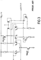
- comparators may also be implemented in integrated circuit form, and a typical example of a prior art integrated comparator is shown in Figure 1 of the accompanying drawings.
- the comparator of Figure 1 comprises a differential cell input stage which includes a first pair of bipolar transistors, of the npn type, connected in a common emitter configuration.
- the bases of these transistors are instead available to serve as circuit inputs, the one for the reference voltage Vr and the other for the input signal Vin, for example.
- a second pair of bipolar transistors, of the pnp type, are associated with the input stage of the comparator.
- the bases of the transistors in this second pair are connected together and receive a bias voltage Vb1.
- the collectors of the first pair of npn transistors are each connected to the corresponding emitter of the second pair of pnp transistors, respectively.
- the comparator output O is taken from the collector of one transistor in the second pair.
- the circuit of Figure 1 exhibits a fairly small dynamic range in the common mode input voltage of about 0.9 Volts.
- the common mode voltage is the highest voltage that can be input without causing anomalous operation of the comparator.
- FIG. 2 A development of the circuit in Figure 1 is shown in Figure 2, where an additional circuit portion is clearly discernible which is basically a follower arrangement and functions as a voltage level shifter.
- That circuit portion comprises a third pair of bipolar transistors, of the common base pnp type, which are connected between the supply Vcc and the signal inputs of the comparator. Each of these transistors is coupled to a resistor having one end connected to a corresponding base terminal of the first transistor pair in the input stage.
- the signal will not be applied to the differential stage directly, but supplied thereto through the follower.
- each resistor will hold the bases of the first transistor pair in the input stage at a suitable voltage for proper operation of these transistors.
- FIG. 3 The circuit depicted in Figure 3 is structurally similar to that shown in Figure 1, except that a second input stage is provided here which comprises a pair of common-emitter pnp bipolar transistors.
- the last-mentioned solution provides a dual differential cell for the input circuit portion, which cell comprises a pair of npn bipolars, on the one side, and a pair of pnp bipolars, on the other.
- the two pairs are connected in parallel through the bases of their respective transistors.
- the first cell is driven by signals at a value close to the supply value Vcc, whereas the second cell operation is referenced to a signal ground value. However, with both transistor pairs in the "off" state, an indefinite condition occurs at the output O.
- This invention pertains to the technical approach represented by the third of the solutions discussed hereinabove.
- the underlying technical problem of this invention is to provide a hysteresis comparator, working with a low voltage, which has such structural and functional features as to overcome the drawbacks of the solutions currently proposed in the prior art and affords expanded dynamic range of the common mode input voltage.
- the solutive idea of the present invention provides for at least one pair of variable current sources associated with each differential cell and tied operatively to the comparator output voltage value.
- a hysteresis comparator circuit embodying this invention.
- This comparator 1 comprises a first differential cell including a first pair of npn-type bipolar transistors T1 and T2 which have their respective emitters in common. Those emitters are also connected to a signal ground GND via a bias current source which comprises a transistor Tn on whose base a voltage Vb3 appears.
- the collectors C1, C2 of the transistors T1, T2 are connected, through respective resistors Rc1 and Rc2, to a power supply line 3 on which a relatively low voltage value Vcc of 1 Volt is present.
- the bases B1, B2 of the transistors T1, T2 are, in turn, connected to the line 3 through respective variable current sources A1, A2.
- current sources are controlled by and tied operatively to the value of the voltage at the output O of the comparator.
- the circuit 1 further comprises a second differential cell 5 including a second transistor pair, T3 and T4.
- This second pair is formed by pnp-type bipolars being, in turn, interconnected with their respective emitters.
- Those emitters are also connected to the supply line 3 via a bias current source which comprises a transistor Tp at whose base a bias voltage Vb1 appears.
- the collectors C3, C4 of the transistors T3, T4 are connected to ground at GND via respective resistors Rc3 and Rc4.
- the bases B3, B4 of the transistors T3, T4 are also connected to ground at GND, via respective variable current sources A3, A4. These current sources are also controlled by and tied operatively to the value of the voltage present at the comparator output O.
- the two differential cells 2 and 5 are coupled together through respective connections between the bases B1, B4 and the bases B2, B3 of the corresponding transistors.
- a voltage divider is connected between each of said base interconnections. Specifically, a first resistor pair R1, R4 are connected between the bases B1, B4, and a second resistor pair R2, R3 are connected between the bases B2 and B3.
- the resistors R1, R2, R3 and R4 have equal values, as equal values have the currents I1, I2 and I3, I4, respectively.
- the point of interconnection of the first resistor pair R1, R4 is the inverting (IN-) input A of the comparator 1.
- the point of interconnection of the second resistor pair R2, R3 is the non-inverting (IN+) input B of the comparator 1.
- the structure of the circuit 1 is completed by a third pair of pnp-type bipolar transistors T9, T11 having corresponding emitters connected directly to the respective collectors C1, C2 of the first transistor pair T1, T2 in the cell 2.
- the transistors T9 and T11 have common-base and are supplied by a base voltage Vb2.
- a fourth bipolar transistor pair T12, T13 of the npn type are provided in association with the second cell 5. Specifically, the transistors T12, T13 which form this fourth pair have corresponding emitters connected directly to the respective collectors C3, C4 of the second transistor pair T3, T4 in the cell 5.
- the transistors T12 and T13 have common-base, and the first, T12, of them has its base connected to the collector to thereby produce a diode configuration.
- the first transistor T9 in the third pair is connected to the first transistor T12 in the fourth pair through the connection between their respective collectors.
- the second transistor T11 in the third pair is connected to the second transistor T13 in the fourth pair through the connection between the respective collectors thereof, and the output O from the comparator circuit 1 is actually taken from the common collector of transistors T11 and T13.
- This output O provides a voltage output value Vo.
- the composite, npn and pnp, structure of the cells 2 and 5 is connected to the signal inputs A and B, through the resistors R1, R2, R3, R4 and the variable current sources A1, A2, A3, A4, and provides a shift in logic level whose value is controlled by the state of the output O.
- the value of the output O also controls, as with any hysteresis comparators, the switching phase between the two (upper and lower) circuit thresholds.
- the current source A1 is suitably sized to ensure proper operation of the first transistor pair in the input stage, and hence an appropriate state of the output O.
- Vin(+) at the non-inverting input B is lower than Vin(-) at the inverting input A.
- Vin(-) could be equal to the upper threshold Vth sup , and the shift level properly selected on the basis of that upper threshold.
- the transistor T1 would operate in the active region until the input voltage Vin(+) attains the upper threshold Vth sup .
- variable source A1 being tied operatively to the output O, is forced to change its outgoing current value by activating the second cell 5 formed by the pnp transistor pair T3 and T4.
- This method of operation affords great freedom of selection of the two discrete threshold levels, thereby expanding the dynamic range of the common mode input voltage.
- variable sources A1 and A2 are embodied by pnp bipolar transistors driven through their respective bases.
- variable sources A3 and A4 are likewise embodied by npn bipolar transistors.
- the output O of the circuit 1 corresponds to the base terminal of an npn transistor T14 having the emitter grounded and the collector connected to the supply Vcc via a current source I.
- the collector of this transistor T14 is connected to the base of an npn transistor T5 having the emitter grounded.
- the base of the transistor T5 also assumes the logic value of negated output O for the comparator 1.
- the collector of the transistor T5 is connected to the respective bases of a set of npn transistors T6, T7, T8 and T10 connected in parallel together, with their emitters grounded.
- the collectors of the transistors T6 and T7 are in common with those of the respective npn transistors incorporated to the current sources A3 and A4.
- the first, T6, in said transistor set has its collector connected to the collector of a further transistor T15, and through the latter, to the base terminals of the pnp transistors incorporated to the current sources A1 and A2.
- a diode D1 connects that collector to the supply Vcc as well.
- the last-mentioned transistor, T15 which is also an npn bipolar type, has its base in common with those of the transistors incorporated to the current sources A3 and A4 and connected between a current source I' associated with the supply Vcc, and a diode D2 connected to ground.
- a similar structure comprising the series of a current source I'' and a diode D3, is associated with the base of the transistor T10.
- the collector of the transistor T10 is connected to the non-inverting input B, whereto the upper voltage threshold value Vth sup is applied via a resistor R5.
- the corresponding negated output O Upon the output O attaining a "high” logic level, the corresponding negated output O will be at a logic "low". Under this condition, the current I'' is allowed to flow through the diode D3 and will be mirrored by the transistor T10 to generate hysteresis of the circuit.
- the shift in logic level is expanded as required for the lower threshold Vth inf .
Landscapes
- Manipulation Of Pulses (AREA)
- Measurement Of Current Or Voltage (AREA)
Priority Applications (4)
| Application Number | Priority Date | Filing Date | Title |
|---|---|---|---|
| DE69320326T DE69320326T2 (de) | 1993-05-07 | 1993-05-07 | Mit niedriger Versorgungsspannung arbeitender, eine Hysteresis aufweisender Komparator |
| EP93830193A EP0623997B1 (fr) | 1993-05-07 | 1993-05-07 | Comparateur à hystérésis avec alimentation à basse tension |
| JP6095287A JPH07142969A (ja) | 1993-05-07 | 1994-05-09 | 集積コンパレータ、ヒステリシス・コンパレータ回路及び電圧差変更方法 |
| US08/240,024 US5563534A (en) | 1993-05-07 | 1994-05-09 | Hysteresis comparator circuit for operation with a low voltage power supply |
Applications Claiming Priority (1)
| Application Number | Priority Date | Filing Date | Title |
|---|---|---|---|
| EP93830193A EP0623997B1 (fr) | 1993-05-07 | 1993-05-07 | Comparateur à hystérésis avec alimentation à basse tension |
Publications (2)
| Publication Number | Publication Date |
|---|---|
| EP0623997A1 true EP0623997A1 (fr) | 1994-11-09 |
| EP0623997B1 EP0623997B1 (fr) | 1998-08-12 |
Family
ID=8215161
Family Applications (1)
| Application Number | Title | Priority Date | Filing Date |
|---|---|---|---|
| EP93830193A Expired - Lifetime EP0623997B1 (fr) | 1993-05-07 | 1993-05-07 | Comparateur à hystérésis avec alimentation à basse tension |
Country Status (4)
| Country | Link |
|---|---|
| US (1) | US5563534A (fr) |
| EP (1) | EP0623997B1 (fr) |
| JP (1) | JPH07142969A (fr) |
| DE (1) | DE69320326T2 (fr) |
Cited By (3)
| Publication number | Priority date | Publication date | Assignee | Title |
|---|---|---|---|---|
| EP0774705A3 (fr) * | 1995-11-16 | 1998-01-28 | Sgs-Thomson Microelectronics Gmbh | Comparateur à hystérésis pour utilisation dans un circuit régulateur de tension |
| EP0862271A2 (fr) * | 1997-02-28 | 1998-09-02 | Siemens Aktiengesellschaft | Circuit comparateur |
| EP0889234A2 (fr) * | 1997-06-30 | 1999-01-07 | Delco Electronics Corporation | Circuit d'entrée de tampon comportant des seuils d'entrées différentiels opérant avec des tensions d'entrées à mode commun élevé |
Families Citing this family (15)
| Publication number | Priority date | Publication date | Assignee | Title |
|---|---|---|---|---|
| US5982639A (en) * | 1997-11-04 | 1999-11-09 | Power Integrations, Inc. | Two switch off-line switching converter |
| US6226190B1 (en) | 1998-02-27 | 2001-05-01 | Power Integrations, Inc. | Off-line converter with digital control |
| US6876181B1 (en) * | 1998-02-27 | 2005-04-05 | Power Integrations, Inc. | Off-line converter with digital control |
| US6107851A (en) | 1998-05-18 | 2000-08-22 | Power Integrations, Inc. | Offline converter with integrated softstart and frequency jitter |
| US6316978B1 (en) | 2000-05-03 | 2001-11-13 | National Semiconductor Corporation | Comparator with process and temperature insensitive hysteresis and threshold potentials |
| US6525514B1 (en) | 2000-08-08 | 2003-02-25 | Power Integrations, Inc. | Method and apparatus for reducing audio noise in a switching regulator |
| US20040183769A1 (en) * | 2000-09-08 | 2004-09-23 | Earl Schreyer | Graphics digitizer |
| JP3914463B2 (ja) * | 2002-05-29 | 2007-05-16 | 株式会社日立製作所 | コンパレータ |
| US7233504B2 (en) | 2005-08-26 | 2007-06-19 | Power Integration, Inc. | Method and apparatus for digital control of a switching regulator |
| US20080106917A1 (en) * | 2006-11-02 | 2008-05-08 | James Holt | Variable edge modulation in a switching regulator |
| US8018694B1 (en) | 2007-02-16 | 2011-09-13 | Fairchild Semiconductor Corporation | Over-current protection for a power converter |
| US7719243B1 (en) | 2007-11-21 | 2010-05-18 | Fairchild Semiconductor Corporation | Soft-start system and method for power converter |
| US7872883B1 (en) | 2008-01-29 | 2011-01-18 | Fairchild Semiconductor Corporation | Synchronous buck power converter with free-running oscillator |
| US7723972B1 (en) | 2008-03-19 | 2010-05-25 | Fairchild Semiconductor Corporation | Reducing soft start delay and providing soft recovery in power system controllers |
| US7902894B2 (en) * | 2009-06-26 | 2011-03-08 | Alpha and Omega Semiconductor Inc. | Accurate hysteretic comparator and method |
Citations (1)
| Publication number | Priority date | Publication date | Assignee | Title |
|---|---|---|---|---|
| US3987368A (en) * | 1974-08-30 | 1976-10-19 | Rca Corporation | Equalization of base current flow in two interconnected transistor amplifiers |
Family Cites Families (24)
| Publication number | Priority date | Publication date | Assignee | Title |
|---|---|---|---|---|
| US4032801A (en) * | 1975-10-10 | 1977-06-28 | Honeywell Inc. | Electromagnetic radiation intensity comparator apparatus |
| US4105901A (en) * | 1976-05-21 | 1978-08-08 | Rca Corporation | Monostable circuit |
| US4147944A (en) * | 1977-10-25 | 1979-04-03 | National Semiconductor Corporation | Comparator with signal related adaptive bias |
| US4401901A (en) * | 1981-06-01 | 1983-08-30 | Advanced Micro Devices, Inc. | Comparator |
| JPS5894225A (ja) * | 1981-11-30 | 1983-06-04 | Sharp Corp | 比較器回路 |
| US4506176A (en) * | 1982-05-26 | 1985-03-19 | Raytheon Company | Comparator circuit |
| AT377136B (de) * | 1982-10-04 | 1985-02-11 | Friedmann & Maier Ag | Elektronischer schalter |
| JPS6054513A (ja) * | 1983-09-06 | 1985-03-29 | Nec Corp | 差動入力コンパレ−タ |
| US4572975A (en) * | 1984-04-02 | 1986-02-25 | Precision Monolithics, Inc. | Analog multiplier with improved linearity |
| US4642484A (en) * | 1985-04-19 | 1987-02-10 | National Semiconductor Corporation | Latching comparator with hysteresis |
| ATE57579T1 (de) * | 1985-12-03 | 1990-11-15 | Siemens Ag | Verfahren und schaltungsanordnung zur pruefung von integrierten schaltungen. |
| DE58906599D1 (de) * | 1989-09-11 | 1994-02-10 | Siemens Ag | Kippschaltung mit Schalthysterese. |
| IT1236692B (it) * | 1989-11-10 | 1993-03-26 | St Microelectronics Srl | Dispositivo elettronico comparatore con isteresi. |
| JPH03173289A (ja) * | 1989-12-01 | 1991-07-26 | Toshiba Corp | 最大値/最小値回路 |
| US5182477A (en) * | 1990-03-22 | 1993-01-26 | Silicon Systems, Inc. | Bipolar tunable transconductance element |
| JP2607729B2 (ja) * | 1990-04-21 | 1997-05-07 | 株式会社東芝 | ヒステリシスコンパレータ |
| US5115151A (en) * | 1990-06-08 | 1992-05-19 | Western Digital Corporation | Triple comparator circuit |
| JP2628785B2 (ja) * | 1990-10-19 | 1997-07-09 | シャープ株式会社 | 出力回路 |
| IT1241394B (it) * | 1990-12-31 | 1994-01-10 | Sgs Thomson Microelectronics | Circuito comparatore con isteresi di precisione ed alta impedenza di ingresso |
| KR930008554A (ko) * | 1991-10-25 | 1993-05-21 | 김광호 | 콤페레이터 |
| JPH0637626A (ja) * | 1992-03-27 | 1994-02-10 | Toshiba Corp | バイアス電流供給回路 |
| KR950008453B1 (ko) * | 1992-03-31 | 1995-07-31 | 삼성전자주식회사 | 내부전원전압 발생회로 |
| US5184028A (en) * | 1992-06-15 | 1993-02-02 | Motorola, Inc. | Current compensating charge pump circuit |
| US5367211A (en) * | 1993-06-28 | 1994-11-22 | Harris Corporation | Differential amplifier with hysteresis |
-
1993
- 1993-05-07 EP EP93830193A patent/EP0623997B1/fr not_active Expired - Lifetime
- 1993-05-07 DE DE69320326T patent/DE69320326T2/de not_active Expired - Fee Related
-
1994
- 1994-05-09 US US08/240,024 patent/US5563534A/en not_active Expired - Lifetime
- 1994-05-09 JP JP6095287A patent/JPH07142969A/ja active Pending
Patent Citations (1)
| Publication number | Priority date | Publication date | Assignee | Title |
|---|---|---|---|---|
| US3987368A (en) * | 1974-08-30 | 1976-10-19 | Rca Corporation | Equalization of base current flow in two interconnected transistor amplifiers |
Non-Patent Citations (2)
| Title |
|---|
| MOTOROLA TECHNICAL DEVELOPMENTS vol. 12, April 1991, SCHAUMBURG, IL., US page 160 G. ALLEN ET AL 'Voltage comparator with hysteresis suitable for low, supply referenced thresholds' * |
| PATENT ABSTRACTS OF JAPAN vol. 7, no. 194 (E-195)(1339) 24 August 1983 & JP-A-58 094 225 ( SHARP K.K. ) 4 June 1983 * |
Cited By (5)
| Publication number | Priority date | Publication date | Assignee | Title |
|---|---|---|---|---|
| EP0774705A3 (fr) * | 1995-11-16 | 1998-01-28 | Sgs-Thomson Microelectronics Gmbh | Comparateur à hystérésis pour utilisation dans un circuit régulateur de tension |
| EP0862271A2 (fr) * | 1997-02-28 | 1998-09-02 | Siemens Aktiengesellschaft | Circuit comparateur |
| EP0862271A3 (fr) * | 1997-02-28 | 1999-11-03 | Siemens Aktiengesellschaft | Circuit comparateur |
| EP0889234A2 (fr) * | 1997-06-30 | 1999-01-07 | Delco Electronics Corporation | Circuit d'entrée de tampon comportant des seuils d'entrées différentiels opérant avec des tensions d'entrées à mode commun élevé |
| EP0889234A3 (fr) * | 1997-06-30 | 2002-05-15 | Delphi Technologies, Inc. | Circuit d'entrée de tampon comportant des seuils d'entrées différentiels opérant avec des tensions d'entrées à mode commun élevé |
Also Published As
| Publication number | Publication date |
|---|---|
| US5563534A (en) | 1996-10-08 |
| DE69320326T2 (de) | 1998-12-24 |
| JPH07142969A (ja) | 1995-06-02 |
| DE69320326D1 (de) | 1998-09-17 |
| EP0623997B1 (fr) | 1998-08-12 |
Similar Documents
| Publication | Publication Date | Title |
|---|---|---|
| EP0623997B1 (fr) | Comparateur à hystérésis avec alimentation à basse tension | |
| US6292031B1 (en) | Level shift circuit with common mode level control | |
| EP0379955A1 (fr) | Circuit ECL et son utilisation en connexion avec un oscillateur contrôlé par voltage | |
| JP2734963B2 (ja) | 低電圧コンパレータ回路 | |
| US5815019A (en) | Flip-flop circuit operating on low voltage | |
| JP2533201B2 (ja) | Am検波回路 | |
| JPH0479171B2 (fr) | ||
| US5349307A (en) | Constant current generation circuit of current mirror type having equal input and output currents | |
| JPH0230902Y2 (fr) | ||
| US6157268A (en) | Voltage controlled emitter coupled multivibrator circuit | |
| EP0096349A1 (fr) | Circuit comparateur | |
| US20020044002A1 (en) | Mixer circuitry | |
| US5262688A (en) | Operational amplifier circuit | |
| JP2646721B2 (ja) | レベル変換回路 | |
| JPH08293785A (ja) | 論理回路 | |
| JPH0749541Y2 (ja) | トランジスタスイッチ回路 | |
| JPH0413695Y2 (fr) | ||
| KR940002237Y1 (ko) | 히스테리시스를 갖는 커런트 모드 비교기 | |
| JP2687160B2 (ja) | スイッチ回路 | |
| EP0374490A2 (fr) | Circuit comparateur de tension pour circuits intégrés d'attaque de charges inductives | |
| JP2797621B2 (ja) | コンパレータ回路 | |
| JPH0434849B2 (fr) | ||
| JPS61140218A (ja) | 入力回路 | |
| GB2302626A (en) | A current source for high voltage operational amplifier output stage | |
| JPH04334120A (ja) | Ecl出力回路 |
Legal Events
| Date | Code | Title | Description |
|---|---|---|---|
| PUAI | Public reference made under article 153(3) epc to a published international application that has entered the european phase |
Free format text: ORIGINAL CODE: 0009012 |
|
| AK | Designated contracting states |
Kind code of ref document: A1 Designated state(s): DE FR GB IT |
|
| 17P | Request for examination filed |
Effective date: 19950421 |
|
| 17Q | First examination report despatched |
Effective date: 19960110 |
|
| GRAG | Despatch of communication of intention to grant |
Free format text: ORIGINAL CODE: EPIDOS AGRA |
|
| GRAG | Despatch of communication of intention to grant |
Free format text: ORIGINAL CODE: EPIDOS AGRA |
|
| GRAH | Despatch of communication of intention to grant a patent |
Free format text: ORIGINAL CODE: EPIDOS IGRA |
|
| ITF | It: translation for a ep patent filed |
Owner name: PORTA CHECCACCI E BOTTI S.R.L. |
|
| GRAH | Despatch of communication of intention to grant a patent |
Free format text: ORIGINAL CODE: EPIDOS IGRA |
|
| GRAA | (expected) grant |
Free format text: ORIGINAL CODE: 0009210 |
|
| AK | Designated contracting states |
Kind code of ref document: B1 Designated state(s): DE FR GB IT |
|
| RAP4 | Party data changed (patent owner data changed or rights of a patent transferred) |
Owner name: STMICROELECTRONICS S.R.L. |
|
| REF | Corresponds to: |
Ref document number: 69320326 Country of ref document: DE Date of ref document: 19980917 |
|
| ET | Fr: translation filed | ||
| PLBE | No opposition filed within time limit |
Free format text: ORIGINAL CODE: 0009261 |
|
| STAA | Information on the status of an ep patent application or granted ep patent |
Free format text: STATUS: NO OPPOSITION FILED WITHIN TIME LIMIT |
|
| 26N | No opposition filed | ||
| REG | Reference to a national code |
Ref country code: GB Ref legal event code: IF02 |
|
| PGFP | Annual fee paid to national office [announced via postgrant information from national office to epo] |
Ref country code: DE Payment date: 20020516 Year of fee payment: 10 |
|
| PG25 | Lapsed in a contracting state [announced via postgrant information from national office to epo] |
Ref country code: DE Free format text: LAPSE BECAUSE OF NON-PAYMENT OF DUE FEES Effective date: 20031202 |
|
| PGFP | Annual fee paid to national office [announced via postgrant information from national office to epo] |
Ref country code: GB Payment date: 20040505 Year of fee payment: 12 |
|
| PGFP | Annual fee paid to national office [announced via postgrant information from national office to epo] |
Ref country code: FR Payment date: 20040510 Year of fee payment: 12 |
|
| PG25 | Lapsed in a contracting state [announced via postgrant information from national office to epo] |
Ref country code: IT Free format text: LAPSE BECAUSE OF NON-PAYMENT OF DUE FEES;WARNING: LAPSES OF ITALIAN PATENTS WITH EFFECTIVE DATE BEFORE 2007 MAY HAVE OCCURRED AT ANY TIME BEFORE 2007. THE CORRECT EFFECTIVE DATE MAY BE DIFFERENT FROM THE ONE RECORDED. Effective date: 20050507 Ref country code: GB Free format text: LAPSE BECAUSE OF NON-PAYMENT OF DUE FEES Effective date: 20050507 |
|
| GBPC | Gb: european patent ceased through non-payment of renewal fee |
Effective date: 20050507 |
|
| PG25 | Lapsed in a contracting state [announced via postgrant information from national office to epo] |
Ref country code: FR Free format text: LAPSE BECAUSE OF NON-PAYMENT OF DUE FEES Effective date: 20060131 |
|
| REG | Reference to a national code |
Ref country code: FR Ref legal event code: ST Effective date: 20060131 |