EP0620651B1 - Method and apparatus for standby recovery in a phase locked loop - Google Patents
Method and apparatus for standby recovery in a phase locked loop Download PDFInfo
- Publication number
- EP0620651B1 EP0620651B1 EP94104687A EP94104687A EP0620651B1 EP 0620651 B1 EP0620651 B1 EP 0620651B1 EP 94104687 A EP94104687 A EP 94104687A EP 94104687 A EP94104687 A EP 94104687A EP 0620651 B1 EP0620651 B1 EP 0620651B1
- Authority
- EP
- European Patent Office
- Prior art keywords
- signal
- output
- counter
- input
- loop
- Prior art date
- Legal status (The legal status is an assumption and is not a legal conclusion. Google has not performed a legal analysis and makes no representation as to the accuracy of the status listed.)
- Expired - Lifetime
Links
- 238000000034 method Methods 0.000 title claims description 7
- 238000011084 recovery Methods 0.000 title claims description 3
- 230000004044 response Effects 0.000 claims description 15
- 230000004913 activation Effects 0.000 claims description 9
- 230000009849 deactivation Effects 0.000 claims description 3
- 230000003213 activating effect Effects 0.000 claims 1
- 230000002779 inactivation Effects 0.000 claims 1
- 230000008859 change Effects 0.000 description 3
- 238000005516 engineering process Methods 0.000 description 3
- 238000004891 communication Methods 0.000 description 2
- 230000000295 complement effect Effects 0.000 description 2
- 238000010586 diagram Methods 0.000 description 2
- 230000001360 synchronised effect Effects 0.000 description 2
- JBRZTFJDHDCESZ-UHFFFAOYSA-N AsGa Chemical compound [As]#[Ga] JBRZTFJDHDCESZ-UHFFFAOYSA-N 0.000 description 1
- 229910001218 Gallium arsenide Inorganic materials 0.000 description 1
- 239000013078 crystal Substances 0.000 description 1
- 238000001514 detection method Methods 0.000 description 1
- 230000004048 modification Effects 0.000 description 1
- 238000012986 modification Methods 0.000 description 1
- 239000004065 semiconductor Substances 0.000 description 1
- 230000007704 transition Effects 0.000 description 1
Images
Classifications
-
- H—ELECTRICITY
- H03—ELECTRONIC CIRCUITRY
- H03L—AUTOMATIC CONTROL, STARTING, SYNCHRONISATION OR STABILISATION OF GENERATORS OF ELECTRONIC OSCILLATIONS OR PULSES
- H03L7/00—Automatic control of frequency or phase; Synchronisation
-
- H—ELECTRICITY
- H03—ELECTRONIC CIRCUITRY
- H03L—AUTOMATIC CONTROL, STARTING, SYNCHRONISATION OR STABILISATION OF GENERATORS OF ELECTRONIC OSCILLATIONS OR PULSES
- H03L7/00—Automatic control of frequency or phase; Synchronisation
- H03L7/06—Automatic control of frequency or phase; Synchronisation using a reference signal applied to a frequency- or phase-locked loop
- H03L7/16—Indirect frequency synthesis, i.e. generating a desired one of a number of predetermined frequencies using a frequency- or phase-locked loop
- H03L7/18—Indirect frequency synthesis, i.e. generating a desired one of a number of predetermined frequencies using a frequency- or phase-locked loop using a frequency divider or counter in the loop
- H03L7/197—Indirect frequency synthesis, i.e. generating a desired one of a number of predetermined frequencies using a frequency- or phase-locked loop using a frequency divider or counter in the loop a time difference being used for locking the loop, the counter counting between numbers which are variable in time or the frequency divider dividing by a factor variable in time, e.g. for obtaining fractional frequency division
- H03L7/199—Indirect frequency synthesis, i.e. generating a desired one of a number of predetermined frequencies using a frequency- or phase-locked loop using a frequency divider or counter in the loop a time difference being used for locking the loop, the counter counting between numbers which are variable in time or the frequency divider dividing by a factor variable in time, e.g. for obtaining fractional frequency division with reset of the frequency divider or the counter, e.g. for assuring initial synchronisation
-
- H—ELECTRICITY
- H03—ELECTRONIC CIRCUITRY
- H03L—AUTOMATIC CONTROL, STARTING, SYNCHRONISATION OR STABILISATION OF GENERATORS OF ELECTRONIC OSCILLATIONS OR PULSES
- H03L7/00—Automatic control of frequency or phase; Synchronisation
- H03L7/06—Automatic control of frequency or phase; Synchronisation using a reference signal applied to a frequency- or phase-locked loop
- H03L7/08—Details of the phase-locked loop
- H03L7/0802—Details of the phase-locked loop the loop being adapted for reducing power consumption
-
- H—ELECTRICITY
- H03—ELECTRONIC CIRCUITRY
- H03L—AUTOMATIC CONTROL, STARTING, SYNCHRONISATION OR STABILISATION OF GENERATORS OF ELECTRONIC OSCILLATIONS OR PULSES
- H03L2207/00—Indexing scheme relating to automatic control of frequency or phase and to synchronisation
- H03L2207/18—Temporarily disabling, deactivating or stopping the frequency counter or divider
Definitions
- This invention relates generally to phase locked loops, and more particularly, to standby methods and circuits for phase locked loops.
- Phase locked loops have important uses in communications applications.
- a PLL frequency synthesizer generates an output signal having a programmable frequency to be used in tuning two or more communication channels.
- a reference oscillator generates a reference signal which is counted in a reference counter to provide a first input of a phase detector.
- An output of a loop counter provides a second input of the phase detector.
- the phase detector provides a voltage indicative of whether the inputs thereof are in lock, i.e. have the same phase and frequency.
- the phase detector output is filtered in a loop filter such as an integrator, the output of which provides an input to a voltage controller oscillator (VCO).
- VCO voltage controller oscillator
- the output of the VCO which is the output of the PLL frequency synthesizer, is then divided in the loop counter. If a different output frequency is desired, the user need only change the starting counter value of the reference counter or the loop counter, and the feedback loop of the PLL frequency synthesizer causes the output frequency to quickly lock.
- the output of the VCO has a relatively large frequency in relation to the reference frequency.
- the VCO may be programmed to output a signal having a frequency of 1.2 gigahertz (GHz). Because this frequency is too high for division in complementary metal-oxide-semiconductor (CMOS) circuitry, the loop counter is usually broken down into two components: a prescaler, and a subsequent counter also referred to as the loop counter. The prescaler can then be made with higher-speed bipolar circuitry, while the loop counter is implemented in CMOS circuitry.
- CMOS complementary metal-oxide-semiconductor
- Low power consumption is a key consideration in many products using PLL frequency synthesizers.
- these products often place the PLL frequency synthesizer in a standby mode to save power.
- the prescaler, counters, and phase detector are disabled to save power.
- the input to the VCO remains substantially constant, causing the VCO output to maintain approximately the same frequency as before the PLL frequency synthesizer entered standby. This creates a problem on exiting standby, however.
- the output of the VCO may have drifted in phase, but not in frequency.
- the counters are re-enabled, they are not synchronized and the phase detector will detect a large error, even though this error reflects a change in phase rather than in frequency. Because of the spurious detection of this large error, the VCO changes its output frequency even though the desired frequency may be correct.
- the PLL takes an undesirably long time to lock.
- U.S. Patent No. 4,841,255 discloses a phase locked loop frequency synthesizer which disconnects a loop filter from a phase comparison section when an intermittent operation signal changes to a low level state. When the intermittent operation signal returns to a high level state, the phase comparison section is reconnected to the loop filter only after three reference periods.
- JP A-1 147 921 discloses a PLL which reduces pull-in time after the end of standby by decoupling a reference frequency signal from the input of a reference divider after the first occurrence of a reference pulse, and recouples the reference frequency signal to the input of the reference divider after the first subsequent frequency division pulse.
- This publication discloses a standby control circuit for a phase locked loop including D flip-flops and various logic gates.
- phase locked loop as claimed in claim 3.
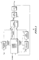
- FIG. 1 illustrates in block diagram form a phase locked loop (PLL) 20 in accordance with the present invention.
- PLL 20 includes a reference counter 21, a prescaler 22, a loop counter 23, a phase detector 24, a loop filter 25, a voltage controlled oscillator 26, and a standby control circuit 30.
- Reference counter 21 has an input for receiving a reference signal labelled "F REF " from a source such as a crystal oscillator (not shown), a control input for receiving a signal labelled "COUNTER ENABLE", and an output for providing an output signal labelled ⁇ R.
- Prescaler 22 has an input for receiving a signal labelled "F VCO '", a control input for receiving COUNTER ENABLE, and an output.
- Loop counter 23 has an input connected to the output of prescaler 22, a control input for receiving COUNTER ENABLE, and an output for providing a signal labelled ⁇ V.
- Phase detector 24 has first and second inputs respectively receiving signals ⁇ R and ⁇ V, a control input for receiving a signal labelled "PHASE DETECTOR ENABLE", and an output for providing a signal labelled "PD OUT ".
- Loop filter 25 has an input for receiving PD OUT , and an output.
- VCO 26 has an input connected to the output terminal of loop filter 25, and an output for providing an output of PLL 20 labelled "F VCO ".
- Standby control circuit 30 has a first input for receiving signal F VCO , a control input for receiving a signal labelled "STANDBY”, and output terminals for providing signals F VCO ', COUNTER ENABLE, and PHASE DETECTOR ENABLE.
- reference counter 21 receives F REF from a reference oscillator (not shown) and counts down from a preprogrammed number to zero. When it reaches a count of zero, reference counter 21 pulses output signal ⁇ R for one period of FREF, and then repeats its counting cycle.
- prescaler 22 counts down from a preprogrammed or predetermined number to zero in response to signal F VCO ' to provide its output for a given number of cycles of F VCO '. The length of time the output of prescaler 22 is active is unimportant because loop counter 23 counts on a low-to-high transition.
- Prescaler 22 is implemented in bipolar technology, and may either be discrete or implemented with CMOS reference counter 21, loop counter 23, and phase detector 24 on a single integrated circuit using bipolar-CMOS (BICMOS) technology. It should be apparent, however, that prescaler 22 may be implemented in any other circuit technology capable of switching at high radio frequencies (RF), typically in the range of 1.2 GHz or beyond, such as gallium arsenide.
- RF radio frequencies
- the output of prescaler 22 drives the input of loop counter 23, which subsequently provides signal ⁇ V.
- the output of VCO 26 is divided by a number determined by the programmed count values of both prescaler 22 and loop counter 23.
- Phase detector 24 is a three-state phase detector which either provides a positive current pulse if ⁇ R leads ⁇ V, provides a negative current pulse if ⁇ V leads ⁇ R or remains in a high impedance state if ⁇ R is in phase with ⁇ V.
- Loop filter 25 is a conventional lowpass loop filter such as an integrator which maintains a history of PD OUT and provides a corresponding voltage to the input of VCO 26 in response.
- VCO 26 provides its output, F VCO , at a frequency proportional to the voltage at the output of loop filter 25.
- Standby control circuit 30 operates to enable and disable the various components of PLL 20 in response to the activation and deactivation of signal STANDBY.
- signal STANDBY is activated (indicating the beginning of standby mode)
- standby control circuit 30 deactivates COUNTER ENABLE and thus reference counter 21, prescaler 22, and loop counter 23 are all disabled.
- Standby mode thus significantly reduces power consumption of CMOS reference counter 21 and CMOS loop counter 23, since power consumption of CMOS circuitry is proportional to switching speed.
- Prescaler 22 may also be designed to operate with reduced power during standby mode by techniques such as placing switches activated by signal STANDBY in series with current sources, interrupting the power supply during standby mode, and the like.
- Standby control circuit 30 also deactivates signal PHASE DETECTOR ENABLE, placing PD OUT in the high impedance state, and maintaining F VCO at the frequency it had at the beginning of standby mode. Standby control circuit 30 passes signal F VCO to its output to provide signal F VCO '.
- standby control circuit 30 When signal STANDBY is deactivated, standby control circuit 30 first activates COUNTER ENABLE. After the first occurrence of ⁇ V, standby control circuit 30 does not pass F VCO to F VCO ', instead driving F VCO ' to a constant logic low value so that prescaler 22 and loop counter 23 do not decrement. Then, after the first occurrence of ⁇ R, standby control circuit 30 activates PHASE DETECTOR ENABLE and gates on F VCO '. At this point, thus, both reference counter 21 and prescaler 22 and loop counter 23 are locked, and assuming there was no frequency drift during standby, PLL 20 is locked.
- PLL 20 operates with low power consumption during standby mode. PLL 20 also recovers from standby mode without spuriously disrupting the output frequency.
- standby control circuit 30 is well-adapted for interface to an off-the-shelf bipolar integrated circuit prescaler that does not have a reset input.
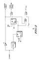
- FIG. 2 illustrates the standby control circuit 30 of FIG. 1.
- Standby control circuit 30 includes an inverter 31, a delay element 32, D-type flip flops 33 and 34, an AND gate 35, an OR gate 36, and an AND gate 37.
- Inverter 31 has an input terminal for receiving signal STANDBY, and an output terminal for providing signal COUNTER ENABLE.
- Delay element 32 has an input terminal for receiving signal STANDBY, and an output terminal.
- Flip flop 33 has a data input terminal labelled "D” connected to a power supply voltage terminal labelled "V SS ", a clock input terminal labelled "CLK” for receiving signal FV, a set input terminal labelled "SET” connected to the output terminal of delay element 32, and a true output terminal labelled "Q".
- V SS is a more-negative power supply voltage terminal which is associated with a logic low voltage level.
- Flip flop 34 has a D input terminal connected to a power supply voltage terminal labelled "V DD ", a CLK input terminal for receiving signal FR, a RST input terminal connected to the Q output terminal of flip flop 33, and a Q output terminal.
- V DD is a more-positive power supply voltage terminal which is associated with a logic high voltage level.
- AND gate 35 has a first input terminal connected to the output terminal of inverter 31, a second input terminal connected to the Q output terminal of flip flop 34, and an output terminal for providing signal PHASE DETECTOR ENABLE.
- OR gate 36 has a first input terminal connected to the Q output terminal of flip flop 34, a second input terminal connected to the Q output terminal of flip flop 33, and an output terminal.
- AND gate 37 has a first input terminal connected to the output terminal of OR gate 36, a second input terminal for receiving signal F VCO , and an output terminal for providing signal F VCO '.
- Standby control circuit 30 activates and deactivates signal COUNTER ENABLE in response to a complement of signal STANDBY through the operation of inverter 31.
- signal STANDBY is activated (indicating a standby state)
- the Q output of flip flop 33 is activated at a logic high voltage, which activates the RST input of flip flop 34.
- Flip flop 34 deactivates its Q output at a logic low, which makes PHASE DETECTOR ENABLE inactive at a logic low regardless of the state of COUNTER ENABLE. Since the Q output of flip flop 33 is at a logic high, the output of OR gate 36 is a logic high.
- the output of AND gate 37 is determined by the state of F VCO , and signal F VCO ' is "gated on”.
- the RST input of flip flop 34 also becomes inactive at a logic low, and the logic high voltage at the D input of flip flop 34 appears on the Q output thereof after the first ⁇ R pulse at the output of reference counter 21.
- AND gate 35 activates signal PHASE DETECTOR ENABLE, and the output of OR gate 36 is driven to a logic high, causing the output of AND gate 37 to change in response to F VCO , and signal F VCO ' is again gated on.
- both reference counter 21 and prescaler 22/loop counter 23 are synchronized at the beginning of their decrement cycles. If VCO 26 has shifted in phase only but not in frequency, thus, PLL 20 has exited standby without causing a frequency error.
- PLL 20 operates with a non-resettable prescaler.
- Delay element 32 eliminates timing problems in standby control circuit 30 and must have a delay of at least one cycle of F REF . This requirement may be accomplished by a series of ratioed inverters sized to guarantee the minimum delay, a one-bit counter connected to F REF , or the like.
- AND gate 37 must be able to switch at the speed of F VCO and may be implemented with a variety of circuits.
- One such circuit is a switched buffer.
- Another such circuit implements the logic function of AND gate 37 as part of a front-end gain stage to prescaler 22.
- This circuit includes a resistor bias network at an input of the gain stage. Two series resistors are connected between the output of OR gate 36 and V SS . The interconnection point of the resistors, which also receives F VCO , is connected to the base of an NPN bipolar transistor, the collector of which provides F VCO .
Landscapes
- Stabilization Of Oscillater, Synchronisation, Frequency Synthesizers (AREA)
Applications Claiming Priority (2)
| Application Number | Priority Date | Filing Date | Title |
|---|---|---|---|
| US08/044,790 US5339278A (en) | 1993-04-12 | 1993-04-12 | Method and apparatus for standby recovery in a phase locked loop |
| US44790 | 1998-03-20 |
Publications (3)
| Publication Number | Publication Date |
|---|---|
| EP0620651A2 EP0620651A2 (en) | 1994-10-19 |
| EP0620651A3 EP0620651A3 (en) | 1995-12-13 |
| EP0620651B1 true EP0620651B1 (en) | 2004-12-22 |
Family
ID=21934353
Family Applications (1)
| Application Number | Title | Priority Date | Filing Date |
|---|---|---|---|
| EP94104687A Expired - Lifetime EP0620651B1 (en) | 1993-04-12 | 1994-03-24 | Method and apparatus for standby recovery in a phase locked loop |
Country Status (7)
| Country | Link |
|---|---|
| US (1) | US5339278A (Direct) |
| EP (1) | EP0620651B1 (Direct) |
| JP (1) | JP2871457B2 (Direct) |
| KR (1) | KR100281156B1 (Direct) |
| CN (1) | CN1033548C (Direct) |
| DE (1) | DE69434193T2 (Direct) |
| TW (1) | TW233393B (Direct) |
Families Citing this family (10)
| Publication number | Priority date | Publication date | Assignee | Title |
|---|---|---|---|---|
| US5497126A (en) * | 1993-11-09 | 1996-03-05 | Motorola, Inc. | Phase synchronization circuit and method therefor for a phase locked loop |
| JPH0879074A (ja) * | 1994-09-05 | 1996-03-22 | Mitsubishi Electric Corp | フェーズ・ロックド・ループ回路 |
| US5548250A (en) * | 1995-01-05 | 1996-08-20 | Cirrus Logic, Inc. | Low power phase lock loop clocking circuit for battery powered systems |
| US5732147A (en) * | 1995-06-07 | 1998-03-24 | Agri-Tech, Inc. | Defective object inspection and separation system using image analysis and curvature transformation |
| US6121845A (en) * | 1998-05-15 | 2000-09-19 | Motorola, Inc. | Phase-locked loop system and method for modifying an output transition time |
| US6150889A (en) | 1998-08-03 | 2000-11-21 | Motorola, Inc. | Circuit and method for minimizing recovery time |
| JP4268726B2 (ja) * | 1999-05-31 | 2009-05-27 | 株式会社ルネサステクノロジ | 半導体装置 |
| SE517967C2 (sv) * | 2000-03-23 | 2002-08-06 | Ericsson Telefon Ab L M | System och förfarande för klocksignalgenerering |
| US9571109B2 (en) * | 2015-03-27 | 2017-02-14 | International Business Machines Corporation | Voltage controlled oscillator runaway prevention |
| CN114499501B (zh) * | 2022-04-19 | 2022-08-26 | 成都市克莱微波科技有限公司 | 一种频率源动态控制方法、控制装置及系统 |
Family Cites Families (19)
| Publication number | Priority date | Publication date | Assignee | Title |
|---|---|---|---|---|
| US3921095A (en) * | 1974-11-14 | 1975-11-18 | Hewlett Packard Co | Startable phase-locked loop oscillator |
| US4005479A (en) * | 1976-01-16 | 1977-01-25 | Control Data Corporation | Phase locked circuits |
| GB1581525A (en) * | 1976-08-04 | 1980-12-17 | Plessey Co Ltd | Frequency synthesis control system |
| US4103250A (en) * | 1977-09-23 | 1978-07-25 | The Bendix Corporation | Fast frequency hopping synthesizer |
| US4330758A (en) * | 1980-02-20 | 1982-05-18 | Motorola, Inc. | Synchronized frequency synthesizer with high speed lock |
| US4521858A (en) * | 1980-05-20 | 1985-06-04 | Technology Marketing, Inc. | Flexible addressing and sequencing system for operand memory and control store using dedicated micro-address registers loaded solely from alu |
| US4378509A (en) * | 1980-07-10 | 1983-03-29 | Motorola, Inc. | Linearized digital phase and frequency detector |
| US4410860A (en) * | 1980-12-31 | 1983-10-18 | Rca Corporation | Frequency synthesizer with learning circuit |
| JPS61258529A (ja) * | 1985-05-13 | 1986-11-15 | Nec Corp | 周波数シンセサイザ |
| JPS6216617A (ja) * | 1985-07-15 | 1987-01-24 | Nec Corp | Pll周波数シンセサイザ |
| CA1282464C (en) * | 1985-10-23 | 1991-04-02 | Masanori Ienaka | Phase-locked oscillator |
| US4714899A (en) * | 1986-09-30 | 1987-12-22 | Motorola, Inc. | Frequency synthesizer |
| CA1290407C (en) * | 1986-12-23 | 1991-10-08 | Shigeki Saito | Frequency synthesizer |
| US4841255A (en) * | 1987-06-24 | 1989-06-20 | Matsushita Electric Industrial Co., Ltd. | Frequency synthesizer |
| US4817199A (en) * | 1987-07-17 | 1989-03-28 | Rockwell International Corporation | Phase locked loop having reduced response time |
| US4918403A (en) * | 1988-06-03 | 1990-04-17 | Motorola, Inc. | Frequency synthesizer with spur compensation |
| US4951005A (en) * | 1989-12-27 | 1990-08-21 | Motorola, Inc. | Phase locked loop with reduced frequency/phase lock time |
| US5075638A (en) * | 1990-12-26 | 1991-12-24 | Motorola, Inc. | Standby system for a frequency synthesizer |
| JP3806230B2 (ja) * | 1997-07-25 | 2006-08-09 | 株式会社多賀製作所 | 半田付方法および装置 |
-
1993
- 1993-04-12 US US08/044,790 patent/US5339278A/en not_active Expired - Lifetime
-
1994
- 1994-03-07 TW TW083101953A patent/TW233393B/zh not_active IP Right Cessation
- 1994-03-24 DE DE69434193T patent/DE69434193T2/de not_active Expired - Lifetime
- 1994-03-24 EP EP94104687A patent/EP0620651B1/en not_active Expired - Lifetime
- 1994-03-30 CN CN94103801A patent/CN1033548C/zh not_active Expired - Lifetime
- 1994-04-01 JP JP6085263A patent/JP2871457B2/ja not_active Expired - Fee Related
- 1994-04-07 KR KR1019940007229A patent/KR100281156B1/ko not_active Expired - Lifetime
Also Published As
| Publication number | Publication date |
|---|---|
| DE69434193T2 (de) | 2005-05-19 |
| JPH0730419A (ja) | 1995-01-31 |
| EP0620651A3 (en) | 1995-12-13 |
| TW233393B (Direct) | 1994-11-01 |
| KR100281156B1 (ko) | 2001-02-01 |
| US5339278A (en) | 1994-08-16 |
| EP0620651A2 (en) | 1994-10-19 |
| CN1033548C (zh) | 1996-12-11 |
| JP2871457B2 (ja) | 1999-03-17 |
| CN1100849A (zh) | 1995-03-29 |
| DE69434193D1 (de) | 2005-01-27 |
| KR940025194A (ko) | 1994-11-19 |
Similar Documents
| Publication | Publication Date | Title |
|---|---|---|
| EP0402736B1 (en) | Phase-difference detecting circuit | |
| US5892380A (en) | Method for shaping a pulse width and circuit therefor | |
| EP0024878B1 (en) | Phase-locked loop circuit | |
| US5180992A (en) | Pll frequency synthesizer having a power saving circuit | |
| CN101931399B (zh) | 一种锁相环频率综合器 | |
| US6150889A (en) | Circuit and method for minimizing recovery time | |
| US20020180540A1 (en) | Lock detection circuit | |
| EP0620651B1 (en) | Method and apparatus for standby recovery in a phase locked loop | |
| KR20130132305A (ko) | 분수 분주형 주파수 합성기의 광범위 멀티-모듈러스 분할기 | |
| CN100376082C (zh) | Pll电路的模式转换方法和pll电路的模式控制电路 | |
| US4771249A (en) | Phase locked loop having a filter with controlled variable bandwidth | |
| US5457428A (en) | Method and apparatus for the reduction of time interval error in a phase locked loop circuit | |
| JP2729196B2 (ja) | 高速5分周回路 | |
| US5132642A (en) | PLL using asynchronously resettable divider to reduce lock time | |
| JP3434794B2 (ja) | Pll回路 | |
| KR100299195B1 (ko) | 가변분주기및위상동기루프회로 | |
| WO2007127574A2 (en) | Phase offset control phase-frequency detector | |
| EP0480597B1 (en) | Phase lock loop | |
| KR100806585B1 (ko) | 위상고정 주파수 합성회로 및 방법 | |
| US7479815B1 (en) | PLL with dual edge sensitivity | |
| CN109150170B (zh) | 锁相环电路 | |
| JPH04297128A (ja) | Pll回路 | |
| JPH07221633A (ja) | 2モジュラスプリスケーラ | |
| JP2002111493A (ja) | Pll回路 | |
| JPH06258465A (ja) | 可変分周回路及びそれを用いた2モジュラス・プリスケーラ |
Legal Events
| Date | Code | Title | Description |
|---|---|---|---|
| PUAI | Public reference made under article 153(3) epc to a published international application that has entered the european phase |
Free format text: ORIGINAL CODE: 0009012 |
|
| AK | Designated contracting states |
Kind code of ref document: A2 Designated state(s): DE FR GB IT |
|
| PUAL | Search report despatched |
Free format text: ORIGINAL CODE: 0009013 |
|
| AK | Designated contracting states |
Kind code of ref document: A3 Designated state(s): DE FR GB IT |
|
| 17P | Request for examination filed |
Effective date: 19960613 |
|
| 17Q | First examination report despatched |
Effective date: 19961227 |
|
| GRAP | Despatch of communication of intention to grant a patent |
Free format text: ORIGINAL CODE: EPIDOSNIGR1 |
|
| GRAS | Grant fee paid |
Free format text: ORIGINAL CODE: EPIDOSNIGR3 |
|
| GRAA | (expected) grant |
Free format text: ORIGINAL CODE: 0009210 |
|
| RAP1 | Party data changed (applicant data changed or rights of an application transferred) |
Owner name: FREESCALE SEMICONDUCTOR, INC. |
|
| AK | Designated contracting states |
Kind code of ref document: B1 Designated state(s): DE FR GB IT |
|
| REG | Reference to a national code |
Ref country code: GB Ref legal event code: FG4D |
|
| REF | Corresponds to: |
Ref document number: 69434193 Country of ref document: DE Date of ref document: 20050127 Kind code of ref document: P |
|
| PLBE | No opposition filed within time limit |
Free format text: ORIGINAL CODE: 0009261 |
|
| STAA | Information on the status of an ep patent application or granted ep patent |
Free format text: STATUS: NO OPPOSITION FILED WITHIN TIME LIMIT |
|
| 26N | No opposition filed |
Effective date: 20050923 |
|
| ET | Fr: translation filed | ||
| PGFP | Annual fee paid to national office [announced via postgrant information from national office to epo] |
Ref country code: GB Payment date: 20130411 Year of fee payment: 20 Ref country code: DE Payment date: 20130408 Year of fee payment: 20 |
|
| PGFP | Annual fee paid to national office [announced via postgrant information from national office to epo] |
Ref country code: IT Payment date: 20130410 Year of fee payment: 20 Ref country code: FR Payment date: 20130417 Year of fee payment: 20 |
|
| REG | Reference to a national code |
Ref country code: DE Ref legal event code: R071 Ref document number: 69434193 Country of ref document: DE |
|
| REG | Reference to a national code |
Ref country code: GB Ref legal event code: PE20 Expiry date: 20140323 |
|
| PG25 | Lapsed in a contracting state [announced via postgrant information from national office to epo] |
Ref country code: GB Free format text: LAPSE BECAUSE OF EXPIRATION OF PROTECTION Effective date: 20140323 Ref country code: DE Free format text: LAPSE BECAUSE OF EXPIRATION OF PROTECTION Effective date: 20140325 |