US4410860A - Frequency synthesizer with learning circuit - Google Patents
Frequency synthesizer with learning circuit Download PDFInfo
- Publication number
- US4410860A US4410860A US06/221,576 US22157680A US4410860A US 4410860 A US4410860 A US 4410860A US 22157680 A US22157680 A US 22157680A US 4410860 A US4410860 A US 4410860A
- Authority
- US
- United States
- Prior art keywords
- frequency
- signal
- vco
- control voltage
- capacitor
- Prior art date
- Legal status (The legal status is an assumption and is not a legal conclusion. Google has not performed a legal analysis and makes no representation as to the accuracy of the status listed.)
- Expired - Fee Related
Links
Images

Classifications
-
- H—ELECTRICITY
- H03—ELECTRONIC CIRCUITRY
- H03L—AUTOMATIC CONTROL, STARTING, SYNCHRONISATION, OR STABILISATION OF GENERATORS OF ELECTRONIC OSCILLATIONS OR PULSES
- H03L7/00—Automatic control of frequency or phase; Synchronisation
- H03L7/06—Automatic control of frequency or phase; Synchronisation using a reference signal applied to a frequency- or phase-locked loop
- H03L7/16—Indirect frequency synthesis, i.e. generating a desired one of a number of predetermined frequencies using a frequency- or phase-locked loop
- H03L7/18—Indirect frequency synthesis, i.e. generating a desired one of a number of predetermined frequencies using a frequency- or phase-locked loop using a frequency divider or counter in the loop
- H03L7/183—Indirect frequency synthesis, i.e. generating a desired one of a number of predetermined frequencies using a frequency- or phase-locked loop using a frequency divider or counter in the loop a time difference being used for locking the loop, the counter counting between fixed numbers or the frequency divider dividing by a fixed number
- H03L7/187—Indirect frequency synthesis, i.e. generating a desired one of a number of predetermined frequencies using a frequency- or phase-locked loop using a frequency divider or counter in the loop a time difference being used for locking the loop, the counter counting between fixed numbers or the frequency divider dividing by a fixed number using means for coarse tuning the voltage controlled oscillator of the loop
- H03L7/189—Indirect frequency synthesis, i.e. generating a desired one of a number of predetermined frequencies using a frequency- or phase-locked loop using a frequency divider or counter in the loop a time difference being used for locking the loop, the counter counting between fixed numbers or the frequency divider dividing by a fixed number using means for coarse tuning the voltage controlled oscillator of the loop comprising a D/A converter for generating a coarse tuning voltage
Definitions
- This invention is concerned with frequency synthesizers, and more particularly, with frequency synthesizers of the type which are preset by a predetermined signal to produce approximately the desired frequency.
- Microwave frequency synthesizers for accurate generation of desired output frequencies are in wide use in the commercial and military communications and radar fields.
- Each of two basic methods for affecting frequency signal synthesis use one or more crystal-controlled oscillators as the basic reference frequencies, and each is digitally programmable in small frequency increments.
- a first direct method uses algebraic manipulation of the one or more reference frequencies to produce the output frequency. This method results in a frequency synthesizer having limited bandwidth, using complex filtering, and being relatively expensive.
- a second indirect method which uses a programmable phase-locked loop for controlling and maintaining a desired output frequency from a voltage controlled oscillator (VCO), is relatively low in cost, covers a wide bandwith, but is relatively slow to respond to a command to change the output frequency of the synthesizer to a desired different frequency value.
- VCO voltage controlled oscillator
- a frequency synthesizer of the phase-locked loop type including means for applying an initial predetermined frequency-control voltage to the VCO. See U.S. Pat. No. 4,105,948, issued Aug. 8, 1978 to H. J. Wolkstein.
- the predetermined control voltage is by necessity only an approximation of that voltage which causes the VCO to produce precisely the desired frequency. Thus time is still consumed by the frequency synthesizer in changing from the approximate frequency due to the predetermined voltage to the precise desired frequency.
- a frequency synthesizer of the phase-locked loop type includes a storage means for storing for each desired frequency that the system can produce a signal value which causes the output frequency producing means to produce exactly the desired frequency.
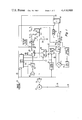
- FIG. 1 is a block diagram of a frequency synthesizer constructed according to the teachings of the invention.
- FIG. 2 is a set of waveforms of various elements in the synthesizer of FIG. 1 and useful in understanding its operation.
- a stable frequency source such as a crystal oscillator 12 is coupled to a frequency multiplier circuit 14 and to a phase comparator circuit 16, each of conventional design.
- the frequency multiplier 14 is coupled to a subtractive mixer 18.
- Mixer 18 also receives an input signal from a coupler 20 which is coupled thereto.
- Coupler 20 is coupled to receive an alternating frequency signal from a voltage controlled oscillator (VCO) 22 or other adjustable frequency source.
- VCO 22 is also coupled to a radiating antenna 24 to transmit into the atmosphere the alternating signal produced by VCO 22.
- Mixer 18 is coupled to a frequency divider circuit 26.
- Divider circuit 26 receives digitally-generated signals on a multi-conductor cable 28 (All multi-conductor cables are designated by a cross hatch symbol such as 30) which are indicative of the frequency of signal desired to be produced by VCO 22.
- Divider circuit 26 is coupled to a second input of phase comparator 16.
- Comparator 16 is coupled via resistor 32 (also designated R 1 ) and pole A and arm C of switch 34 to a capacitor 36 (also designated C) and to an amplifier 38.
- Amplifier 38 which may or may not have gain and may or may not provide direct current offset depending on the parameters of the system components, is coupled to the control terminal of VCO 22 to control the frequency of signals produced thereby.
- Resistor 32 and capacitor 36 together form an RC time constant circuit.
- VCO 22 is expected to produce a frequency in the range from 10,005 to 10,500 MHz in increments of 5 MHz.
- crystal oscillator 12 produces a signal of the incremental frequency, i.e., 5 MHz.
- Frequency multiplier 14 multiplies the crystal oscillator frequency to produce a frequency value which is near but outside the range of frequencies produced by VCO 22. With an examplary multiplication factor of 2,000, the resulting frequency multiplied signal of 10,000 MHz is subtractively mixed in mixer 18 with the signal produced by VCO 22 having a value between the range of 10,005 MHz to 10,500 MHz.
- the resultant signal produced by mixer 18 having a value in the range of 5 to 500 MHz is divided by divider 26 by a value corresponding to the desired frequency output of VCO 22 as indicated by signals applied on line 28 to circuit 26.
- the output of circuit 26 is such that when the VCO is producing a desired frequency, circuit 26 produces a 5 MHz signal equal to that produced by oscillator 12.
- circuit 26 divides by 100.
- VCO 22 is to produce 10,005 MHz
- circuit 26 divides by 1, again to ideally produce an output of 5 MHz.
- phase comparator 16 produces on line 16a thereof typically either no signal or a signal alternating between a high value and a low value at a 50 percent duty cycle.
- phase comparator 16 produces on line 16a a relatively negative signal or a signal in which the low value portion of the alternating high and low signal is emphasized over the high value portion, assuming that VCO 22 has a positive transfer function (i.e., an increase of control voltage produces an increase of output frequency).
- phase comparator 16 produces on line 16a a relatively positive signal or a signal in which the high value portion of the alternating high and low signal is emphasized over the low value portion.
- the signal produced on line 16a charges or discharges capacitor 36 according to the rate determined by the time constant value of C and R 1 .
- a relatively large time constant of R 1 and C results in a relatively long time for VCO 22 to stabilize at a new frequency, but the VCO output will become very stable.
- a relatively small time constant of R 1 and C results in a relatively short time for VCO 22 to lock at a new frequency, but the VCO output is rather unstable, tending to hunt about the desired frequency.
- arm C of switch 34 is coupled to a sample-and-hold circuit (S/H) 40.
- S/H 40 is coupled to an analog-to-digital circuit (A/D) 42 which is coupled to a random access memory (RAM) 44 to provide information thereto.
- RAM 44 is coupled to a temporary holding register 46 and to the common (C) arm of a single-pole-double throw switch 48.
- switch 48 like switch 34, is in reality, a solid state device but is shown as a mechanical switch for schematic simplification.
- Temporary holding register 46 is coupled to a digital-to-analog converter (D/A) 50 for the conversion of digital information stored in temporary holding register 46 to an analog voltage level.
- D/A 50 is coupled via resistor 52 (also designated R 2 ), to terminal B of single-pole double-throw switch 34.
- resistor 52 is much less than the value of resistor 32. In fact, resistor 52 may be just the resistance of the interconnection between D/A 50 and capacitor 36 added to the resistance of the output circuit of D/A 50.
- terminal 60 receives a "change frequency" pulse from a source (not shown) whenever it is desired to change the frequency produced by VCO 22.
- Terminal 60 is coupled to the control terminal of each of a control logic means 62, a source of signal indicative of desired frequencies 64, a temporary storage means 66 for storing the current frequency, via a delay 68 to one terminal of an OR gate 70, to the reset (R) terminal of a J-K flip-flop 74 and to temporary holding register 46.
- Comparator 16 produces a signal on line 16b when it is locked, that is, when the signal produced by oscillator 12 and circuit 26 are of the same frequency and phase.
- Line 16b is connected to OR gate 70.
- OR gate 70 is coupled to the set (S) terminal of flip-flop 74.
- the Q terminal of flip-flop 74 is coupled to control logic block 62.
- Control logic block 62 is basically a timing means which is responsive to input signals from terminal 60, flip-flop 74 and A/D 42 to produce at pre-selected times thereafter, signals which are applied to control terminals of S/H 40, A/D 42, switches 34 and 48 and to the read/write (R/W) terminal of RAM 44.
- the timing of signals applied to control logic block 62 and produced by control logic block 62 is as indicated in FIG. 2, which will be referred to in connection with a description of the operation of the system of FIG. 1.
- Control logic block 62 may consist of a series of pre-selected delays or a master clock source and counters reset by th various inputs and designed to produce outputs at pre-selected counts.
- Desired frequency block 64 is any suitable source of digital indication of frequency to be produced by VCO 22, such as, for example, a computer or preset switches. Each time desired frequency block 64 receives a change frequency pulse from terminal 60 it changes to the next frequency which may be the same as or different from the preceding frequency. Block 64 is coupled to the A pole of switch 48 and to the input terminal of temporary storage means 66 for storing the previous frequency indication produced by block 64 and which, as will be described is the current frequency being produced by VCO 22. For example, if block 64 is producing an indication of a frequency F 1 and a change frequency pulse occurs, the indication of frequency F 1 will be stored in temporary storage means 66 while an indication of a new frequency F 2 will be stored in block 64, both under control of the change frequency pulse.
- waveform A FIG. 2
- P which, for example, may be, 50 microseconds.
- desired frequency block 64 is producing a signal indicative of a frequency F 1 which is the frequency which VCO 22 is to produce after waveform 2A, pulse 80, is generated.
- switches 32 and 48 are positioned as shown, that is, with common arm C connected to pole A and that for each frequency that VCO 22 can assume an associated RAM 44 storage location stores a digital number which when converted to an analog value is of such a value as to cause VCO 22 to produce approximagtely or exactly the desired frequency.
- pulse 80 When pulse 80, waveform 2A, occurs, it causes an indication of frequency F 1 to be stored in temporary storage 66 from block 64, causes the digital value stored in RAM 44 at the address determined by the digital value corresponding to F 1 as stored in block 64, to be transmitted to holding register 46, where the value stored in RAM 44 is the digital equivalent of a voltage which will cause VCO 22 to produce frequency F 1 , and causes the next desired frequency F 2 to be produced in block 64.
- the value in block 64 causes RAM 44 to be addressed to produce the digital value, the analog equivalent of which will cause VCO to produce frequency F 2 .
- the digital equivalent of F 1 is stored in temporary holding register 46 where it remains until the next change frequency pulse 82, waveform 2A, occurs. Further, pulse 80 resets flip-flop 74 and starts timing activities in control logic 62.
- control logic 62 Immediately upon receipt of pulse 80, control logic 62 produces a pulse, waveform 2D, which causes switch 34, arm C, to contact pole B at which time D/A 50 is producing an analog voltage which will cause VCO 22 to produce frequency F 1 . Because resistor 52 is very small and therefore the R 2 C time constant is very small, following pulse 80, waveform 2A, VCO 22 quickly produces a frequency near and perhaps equal to frequency F 1 . As known to those skilled in the art, the voltage applied to VCO 22 will be within 99 percent of the voltage produced by D/A 50 within 5 R 2 C time constants. Then under control of control logic 62, switch 34 is reset to the position illustrated in FIG. 1; that is, with arm C in contact with pole A, and the normal phase-locked loop operation previously discussed resumes with VCO 22 attaining and maintaining frequency F 1 .
- phase comparator 16 determines that VCO 22 is producing frequency F 1 , a pulse indicative of that fact is produced on line 16b and causes flip-flop 74 to set. See waveform 2G, pulse 90. Pulses such as 90 indicate comparator 16 is locked.
- control logic 62 causes S/H 40 to hold the voltage it is sampling and causes A/D 42 to digitize that voltage.
- A/D 42 is producing a stable output an indication pulse is sent to control logic 62 (see waveform 2H, pulse 96).
- control logic 62 causes switch 48 to change state such that arm C is in contact with pole B.
- RAM 44 is addressed at its location which corresponds to the current frequency F 1 set in temporary store 66.
- RAM 44 is stable the value stored in S/H 40 is stored in RAM 44 under control of a write signal applied on line 44a to RAM 44. See waveform 2K.
- switch 48 is reset to the position illustrated in FIG. 1, that is, with arm C in contact with pole A and RAM 44 is again addressed in the read mode to produce a value equal to F 2 .
- RAM 44 contains at a storage location corresponding to frequency F 1 a digital value equal to the precise voltage which causes VCO 22 to produce F 1 .
- RAM 44 will be storing a value which will cause VC0 22 to produce exactly frequency F 1 from the beginning.
- the phase of the signals supplied to comparator 16 must still be made to coincide.
- the change frequency pulse via delay 68 will set flip-flop 74 and the above-described procedure will repeat.
- Such action which is illustrated in FIG. 2 between pulses 82 and 84 of waveform A, is likely to occur when the synthesizer is first activated before RAM 44 contains proper data.
- the amount of delay in delay 68 may be set to any desired value such that there is ample time to write data into RAM 44 and to have it set to the readout value of the next frequency before the next change frequency pulse, such as pulse 84, waveform 2A, occurs. As illustrated in the waveforms of FIG.
- RAM 44 does not contain the exact indication of the associated frequency but contains a value which approximates the desired frequency more closely than would be true in the absence of the invention.
- a learning process occurs in that several iterations of each frequency must occur before RAM 44 contains the correct value for each of the desired frequencies.
Abstract
Description
Claims (10)
Priority Applications (1)
| Application Number | Priority Date | Filing Date | Title |
|---|---|---|---|
| US06/221,576 US4410860A (en) | 1980-12-31 | 1980-12-31 | Frequency synthesizer with learning circuit |
Applications Claiming Priority (1)
| Application Number | Priority Date | Filing Date | Title |
|---|---|---|---|
| US06/221,576 US4410860A (en) | 1980-12-31 | 1980-12-31 | Frequency synthesizer with learning circuit |
Publications (1)
| Publication Number | Publication Date |
|---|---|
| US4410860A true US4410860A (en) | 1983-10-18 |
Family
ID=22828370
Family Applications (1)
| Application Number | Title | Priority Date | Filing Date |
|---|---|---|---|
| US06/221,576 Expired - Fee Related US4410860A (en) | 1980-12-31 | 1980-12-31 | Frequency synthesizer with learning circuit |
Country Status (1)
| Country | Link |
|---|---|
| US (1) | US4410860A (en) |
Cited By (22)
| Publication number | Priority date | Publication date | Assignee | Title |
|---|---|---|---|---|
| US4538149A (en) * | 1982-01-18 | 1985-08-27 | The United States Of America As Represented By The Secretary Of The Navy | Frequency agile magnetron imaging radar |
| US4547775A (en) * | 1982-01-18 | 1985-10-15 | The United States Of America As Represented By The Secretary Of The Navy | Frequency agile imaging radar with error frequency correction |
| FR2563666A1 (en) * | 1984-05-01 | 1985-10-31 | Tadiran Ltd | FREQUENCY SYNTHESIZER FOR MILLIMETER WAVES |
| US4562411A (en) * | 1983-12-29 | 1985-12-31 | Rca Corporation | Prepositioning circuit for phase lock loop |
| US4562410A (en) * | 1983-12-29 | 1985-12-31 | Rca Corporation | Phase lock loop prepositioning apparatus with feedback control |
| US4568888A (en) * | 1983-11-08 | 1986-02-04 | Trw Inc. | PLL Fast frequency synthesizer with memories for coarse tuning and loop gain correction |
| EP0182549A1 (en) * | 1984-11-07 | 1986-05-28 | Shaye Communications Limited | Radio frequency synthesis |
| GB2197143A (en) * | 1986-11-01 | 1988-05-11 | Gen Electric Plc | Phase-lock loop test-signal generator |
| EP0360442A1 (en) * | 1988-09-02 | 1990-03-28 | Nippon Telegraph and Telephone Corporation | Frequency sythesizer |
| EP0406469A1 (en) * | 1989-07-06 | 1991-01-09 | Deutsche ITT Industries GmbH | Digital control circuit for tuning systems |
| EP0412491A2 (en) * | 1989-08-10 | 1991-02-13 | Mitsubishi Denki Kabushiki Kaisha | Frequency Synthesizer |
| US5027087A (en) * | 1990-02-02 | 1991-06-25 | Motorola, Inc. | Fast-switching frequency synthesizer |
| EP0471502A1 (en) * | 1990-08-13 | 1992-02-19 | Fujitsu Limited | Phase locked loop circuit and semiconductor integrated circuit using the phase locked loop circuit |
| US5207491A (en) * | 1991-01-31 | 1993-05-04 | Motorola Inc. | Fast-switching frequency synthesizer |
| US5304956A (en) * | 1992-07-17 | 1994-04-19 | Trw Inc. | Low noise high speed frequency synthesizer employing a learning sequence |
| US5339278A (en) * | 1993-04-12 | 1994-08-16 | Motorola, Inc. | Method and apparatus for standby recovery in a phase locked loop |
| US5367269A (en) * | 1990-11-08 | 1994-11-22 | Pioneer Electronic Corporation | System for producing an oscillating jamming signal utilizing a phase-locked loop |
| US5414741A (en) * | 1993-10-14 | 1995-05-09 | Litton Systems, Inc. | Low phase noise oscillator frequency control apparatus and method |
| US6380809B1 (en) * | 2000-02-18 | 2002-04-30 | Ericsson Inc. | Method and apparatus for tuning oscillator to a selected frequency |
| US6714085B1 (en) | 2002-10-24 | 2004-03-30 | General Dynamics Decision Systems, Inc | Prepositioned frequency synthesizer and method therefor |
| US20060158262A1 (en) * | 2005-01-20 | 2006-07-20 | Robinson Michael A | Offset correction in a feedback system for a voltage controlled oscillator |
| US20060208808A1 (en) * | 2005-03-07 | 2006-09-21 | Samsung Electronics Co., Ltd. | Method and system for calibrating input voltage of voltage controlled oscillator and digital interface used for calibrating input voltage |
Citations (4)
| Publication number | Priority date | Publication date | Assignee | Title |
|---|---|---|---|---|
| US3675146A (en) * | 1971-03-08 | 1972-07-04 | J Michael Langham | Digital variable frequency oscillator |
| US3753142A (en) * | 1972-06-12 | 1973-08-14 | Logimetrics Inc | Signal generators employing digital phase locked loops and compensating circuits |
| US3927384A (en) * | 1974-08-20 | 1975-12-16 | Itt | Frequency synthesizer |
| US4272729A (en) * | 1979-05-10 | 1981-06-09 | Harris Corporation | Automatic pretuning of a voltage controlled oscillator in a frequency synthesizer using successive approximation |
-
1980
- 1980-12-31 US US06/221,576 patent/US4410860A/en not_active Expired - Fee Related
Patent Citations (4)
| Publication number | Priority date | Publication date | Assignee | Title |
|---|---|---|---|---|
| US3675146A (en) * | 1971-03-08 | 1972-07-04 | J Michael Langham | Digital variable frequency oscillator |
| US3753142A (en) * | 1972-06-12 | 1973-08-14 | Logimetrics Inc | Signal generators employing digital phase locked loops and compensating circuits |
| US3927384A (en) * | 1974-08-20 | 1975-12-16 | Itt | Frequency synthesizer |
| US4272729A (en) * | 1979-05-10 | 1981-06-09 | Harris Corporation | Automatic pretuning of a voltage controlled oscillator in a frequency synthesizer using successive approximation |
Cited By (30)
| Publication number | Priority date | Publication date | Assignee | Title |
|---|---|---|---|---|
| US4547775A (en) * | 1982-01-18 | 1985-10-15 | The United States Of America As Represented By The Secretary Of The Navy | Frequency agile imaging radar with error frequency correction |
| US4538149A (en) * | 1982-01-18 | 1985-08-27 | The United States Of America As Represented By The Secretary Of The Navy | Frequency agile magnetron imaging radar |
| US4568888A (en) * | 1983-11-08 | 1986-02-04 | Trw Inc. | PLL Fast frequency synthesizer with memories for coarse tuning and loop gain correction |
| US4562411A (en) * | 1983-12-29 | 1985-12-31 | Rca Corporation | Prepositioning circuit for phase lock loop |
| US4562410A (en) * | 1983-12-29 | 1985-12-31 | Rca Corporation | Phase lock loop prepositioning apparatus with feedback control |
| US4614917A (en) * | 1984-05-01 | 1986-09-30 | Tadiran Ltd. | Millimeter wave frequency synthesizer with automatic loop gain correction and sophisticated lock search systems |
| FR2563666A1 (en) * | 1984-05-01 | 1985-10-31 | Tadiran Ltd | FREQUENCY SYNTHESIZER FOR MILLIMETER WAVES |
| EP0182549A1 (en) * | 1984-11-07 | 1986-05-28 | Shaye Communications Limited | Radio frequency synthesis |
| GB2197143A (en) * | 1986-11-01 | 1988-05-11 | Gen Electric Plc | Phase-lock loop test-signal generator |
| EP0360442A1 (en) * | 1988-09-02 | 1990-03-28 | Nippon Telegraph and Telephone Corporation | Frequency sythesizer |
| US4980652A (en) * | 1988-09-02 | 1990-12-25 | Nippon Telegraph And Telephone Corporation | Frequency synthesizer having compensation for nonlinearities |
| EP0406469A1 (en) * | 1989-07-06 | 1991-01-09 | Deutsche ITT Industries GmbH | Digital control circuit for tuning systems |
| US5059979A (en) * | 1989-07-06 | 1991-10-22 | Deutsche Itt Industries Gmbh | Digital control circuit for tuning systems with a pulse density modulation digital to analog converter |
| EP0412491A2 (en) * | 1989-08-10 | 1991-02-13 | Mitsubishi Denki Kabushiki Kaisha | Frequency Synthesizer |
| EP0412491A3 (en) * | 1989-08-10 | 1991-10-02 | Mitsubishi Denki Kabushiki Kaisha | Frequency synthesizer |
| WO1991011852A1 (en) * | 1990-02-02 | 1991-08-08 | Motorola, Inc. | Fast-switching frequency synthesizer |
| AU633228B2 (en) * | 1990-02-02 | 1993-01-21 | Motorola, Inc. | Fast-switching frequency synthesizer |
| US5027087A (en) * | 1990-02-02 | 1991-06-25 | Motorola, Inc. | Fast-switching frequency synthesizer |
| EP0471502A1 (en) * | 1990-08-13 | 1992-02-19 | Fujitsu Limited | Phase locked loop circuit and semiconductor integrated circuit using the phase locked loop circuit |
| US5367269A (en) * | 1990-11-08 | 1994-11-22 | Pioneer Electronic Corporation | System for producing an oscillating jamming signal utilizing a phase-locked loop |
| US5207491A (en) * | 1991-01-31 | 1993-05-04 | Motorola Inc. | Fast-switching frequency synthesizer |
| US5304956A (en) * | 1992-07-17 | 1994-04-19 | Trw Inc. | Low noise high speed frequency synthesizer employing a learning sequence |
| US5339278A (en) * | 1993-04-12 | 1994-08-16 | Motorola, Inc. | Method and apparatus for standby recovery in a phase locked loop |
| US5414741A (en) * | 1993-10-14 | 1995-05-09 | Litton Systems, Inc. | Low phase noise oscillator frequency control apparatus and method |
| US6380809B1 (en) * | 2000-02-18 | 2002-04-30 | Ericsson Inc. | Method and apparatus for tuning oscillator to a selected frequency |
| US6714085B1 (en) | 2002-10-24 | 2004-03-30 | General Dynamics Decision Systems, Inc | Prepositioned frequency synthesizer and method therefor |
| US20060158262A1 (en) * | 2005-01-20 | 2006-07-20 | Robinson Michael A | Offset correction in a feedback system for a voltage controlled oscillator |
| US7173494B2 (en) * | 2005-01-20 | 2007-02-06 | Avago Technologies General Ip (Singapore) Pte. Ltd. | Method and system for operating a feedback system for a voltage controlled oscillator that involves correcting for offset related to the feedback system |
| US20060208808A1 (en) * | 2005-03-07 | 2006-09-21 | Samsung Electronics Co., Ltd. | Method and system for calibrating input voltage of voltage controlled oscillator and digital interface used for calibrating input voltage |
| US7301406B2 (en) * | 2005-03-07 | 2007-11-27 | Samsung Electronics Co., Ltd. | Method and system for calibrating input voltage of voltage controlled oscillator and digital interface used for calibrating input voltage |
Similar Documents
| Publication | Publication Date | Title |
|---|---|---|
| US4410860A (en) | Frequency synthesizer with learning circuit | |
| US4099137A (en) | High speed phase lock control for frequency switching | |
| US4103250A (en) | Fast frequency hopping synthesizer | |
| US4105948A (en) | Frequency synthesizer with rapidly changeable frequency | |
| CA1054232A (en) | Phase detector having a 360.degree. linear range for periodic and aperiodic input pulse streams | |
| US3621403A (en) | Digital frequency modulated sweep generator | |
| US3364437A (en) | Precision swept oscillator | |
| US4442412A (en) | Phase locked-loop generator with closed-loop forcing function shaper | |
| US4684897A (en) | Frequency correction apparatus | |
| US4849714A (en) | Signal generating apparatus | |
| US4160958A (en) | Sampling linearizer utilizing a phase shifter | |
| GB2041682A (en) | Digital frequency lock tuning system | |
| US4560960A (en) | Digital frequency synthesizer for generating a frequency-modulated signal and radio frequency apparatus including such a device | |
| US4244027A (en) | Digital open loop programmable frequency multiplier | |
| US3760280A (en) | Method and apparatus for delaying an electrical signal | |
| EP0459446A1 (en) | Numerical controlled oscillator | |
| JPS6111003B2 (en) | ||
| US3997764A (en) | Method for the conversion of a frequency into a number | |
| US4079371A (en) | Rate converter for digital signals having a negative feedback phase lock loop | |
| US4502105A (en) | Inverter firing control with pulse averaging error compensation | |
| US3723907A (en) | Sync oscillator | |
| US4546328A (en) | PLL Swept frequency generator with programmable sweep rate | |
| US4724421A (en) | Time interval to digital converter with smoothing | |
| US3546618A (en) | Low power,high stability digital frequency synthesizer | |
| USRE34831E (en) | Communication system |
Legal Events
| Date | Code | Title | Description |
|---|---|---|---|
| MAFP | Maintenance fee payment |
Free format text: PAYMENT OF MAINTENANCE FEE, 4TH YEAR, PL 96-517 (ORIGINAL EVENT CODE: M170); ENTITY STATUS OF PATENT OWNER: LARGE ENTITY Year of fee payment: 4 |
|
| MAFP | Maintenance fee payment |
Free format text: PAYMENT OF MAINTENANCE FEE, 8TH YEAR, PL 96-517 (ORIGINAL EVENT CODE: M171); ENTITY STATUS OF PATENT OWNER: LARGE ENTITY Year of fee payment: 8 |
|
| FEPP | Fee payment procedure |
Free format text: PAYOR NUMBER ASSIGNED (ORIGINAL EVENT CODE: ASPN); ENTITY STATUS OF PATENT OWNER: LARGE ENTITY |
|
| AS | Assignment |
Owner name: MARTIN MARIETTA CORPORATION, MARYLAND Free format text: ASSIGNMENT OF ASSIGNORS INTEREST;ASSIGNOR:GENERAL ELECTRIC COMPANY;REEL/FRAME:007046/0736 Effective date: 19940322 |
|
| FEPP | Fee payment procedure |
Free format text: MAINTENANCE FEE REMINDER MAILED (ORIGINAL EVENT CODE: REM.); ENTITY STATUS OF PATENT OWNER: LARGE ENTITY |
|
| LAPS | Lapse for failure to pay maintenance fees | ||
| FP | Lapsed due to failure to pay maintenance fee |
Effective date: 19951018 |
|
| AS | Assignment |
Owner name: LOCKHEED MARTIN CORPORATION, MARYLAND Free format text: ASSIGNMENT OF ASSIGNORS INTEREST;ASSIGNOR:MARTIN MARIETTA CORPORATION;REEL/FRAME:008628/0518 Effective date: 19960128 |
|
| STCH | Information on status: patent discontinuation |
Free format text: PATENT EXPIRED DUE TO NONPAYMENT OF MAINTENANCE FEES UNDER 37 CFR 1.362 |