EP0618657B1 - Automatische Triggerschaltung - Google Patents
Automatische Triggerschaltung Download PDFInfo
- Publication number
- EP0618657B1 EP0618657B1 EP94400736A EP94400736A EP0618657B1 EP 0618657 B1 EP0618657 B1 EP 0618657B1 EP 94400736 A EP94400736 A EP 94400736A EP 94400736 A EP94400736 A EP 94400736A EP 0618657 B1 EP0618657 B1 EP 0618657B1
- Authority
- EP
- European Patent Office
- Prior art keywords
- transistor
- transistors
- floating
- voltage
- grid
- Prior art date
- Legal status (The legal status is an assumption and is not a legal conclusion. Google has not performed a legal analysis and makes no representation as to the accuracy of the status listed.)
- Expired - Lifetime
Links
- 238000001514 detection method Methods 0.000 claims description 17
- 230000001105 regulatory effect Effects 0.000 claims 3
- 238000004519 manufacturing process Methods 0.000 description 14
- 238000007667 floating Methods 0.000 description 10
- 230000008901 benefit Effects 0.000 description 4
- 230000008859 change Effects 0.000 description 4
- 239000003990 capacitor Substances 0.000 description 2
- 230000008878 coupling Effects 0.000 description 2
- 238000010168 coupling process Methods 0.000 description 2
- 238000005859 coupling reaction Methods 0.000 description 2
- 238000002347 injection Methods 0.000 description 2
- 239000007924 injection Substances 0.000 description 2
- 230000007257 malfunction Effects 0.000 description 2
- 238000005259 measurement Methods 0.000 description 2
- 230000007423 decrease Effects 0.000 description 1
- 238000009795 derivation Methods 0.000 description 1
- 238000010586 diagram Methods 0.000 description 1
- 239000006185 dispersion Substances 0.000 description 1
- 230000005684 electric field Effects 0.000 description 1
- 238000005516 engineering process Methods 0.000 description 1
- 238000002513 implantation Methods 0.000 description 1
- 239000012535 impurity Substances 0.000 description 1
- 230000014759 maintenance of location Effects 0.000 description 1
- 238000000034 method Methods 0.000 description 1
- 239000000243 solution Substances 0.000 description 1
- 230000001960 triggered effect Effects 0.000 description 1
Images


Classifications
-
- H—ELECTRICITY
- H02—GENERATION; CONVERSION OR DISTRIBUTION OF ELECTRIC POWER
- H02H—EMERGENCY PROTECTIVE CIRCUIT ARRANGEMENTS
- H02H3/00—Emergency protective circuit arrangements for automatic disconnection directly responsive to an undesired change from normal electric working condition with or without subsequent reconnection ; integrated protection
- H02H3/20—Emergency protective circuit arrangements for automatic disconnection directly responsive to an undesired change from normal electric working condition with or without subsequent reconnection ; integrated protection responsive to excess voltage
- H02H3/207—Emergency protective circuit arrangements for automatic disconnection directly responsive to an undesired change from normal electric working condition with or without subsequent reconnection ; integrated protection responsive to excess voltage also responsive to under-voltage
-
- G—PHYSICS
- G01—MEASURING; TESTING
- G01R—MEASURING ELECTRIC VARIABLES; MEASURING MAGNETIC VARIABLES
- G01R19/00—Arrangements for measuring currents or voltages or for indicating presence or sign thereof
- G01R19/165—Indicating that current or voltage is either above or below a predetermined value or within or outside a predetermined range of values
- G01R19/16566—Circuits and arrangements for comparing voltage or current with one or several thresholds and for indicating the result not covered by subgroups G01R19/16504, G01R19/16528, G01R19/16533
- G01R19/1659—Circuits and arrangements for comparing voltage or current with one or several thresholds and for indicating the result not covered by subgroups G01R19/16504, G01R19/16528, G01R19/16533 to indicate that the value is within or outside a predetermined range of values (window)
-
- G—PHYSICS
- G11—INFORMATION STORAGE
- G11C—STATIC STORES
- G11C16/00—Erasable programmable read-only memories
- G11C16/02—Erasable programmable read-only memories electrically programmable
- G11C16/06—Auxiliary circuits, e.g. for writing into memory
- G11C16/22—Safety or protection circuits preventing unauthorised or accidental access to memory cells
- G11C16/225—Preventing erasure, programming or reading when power supply voltages are outside the required ranges
-
- H—ELECTRICITY
- H02—GENERATION; CONVERSION OR DISTRIBUTION OF ELECTRIC POWER
- H02H—EMERGENCY PROTECTIVE CIRCUIT ARRANGEMENTS
- H02H3/00—Emergency protective circuit arrangements for automatic disconnection directly responsive to an undesired change from normal electric working condition with or without subsequent reconnection ; integrated protection
- H02H3/006—Calibration or setting of parameters
Definitions
- the present invention relates to an automatic tripping circuit, in particular a reset circuit, usable in any electronic circuit.
- the invention is intended to be used more particularly in the field of smart cards. However, it can be used in all fields where power supply standards are intended to evolve due to technological improvements in electronic circuits.
- a notion of security must be considered. Indeed, a smart card must work correctly not only within a specified supply voltage range, but also outside this range for prevent, for example, a potential fraudster from taking advantage of a malfunction outside this range to discover the secrets of the card and / or to modify its stored content, for example adding monetary units. To protect against these attempts, most integrated circuits are equipped with trigger circuits which block the operation of the card outside a certain voltage range.
- trigger thresholds equal to approximately 2 Volts and 7 Volts. But with temperature and changes in manufacturing parameters, these thresholds can vary by themselves between 1.5 and 2.5 Volts and between 6 and 8 Volts.
- the object of the invention is therefore to arrive at constructing a trigger circuit stable in threshold voltage, and adjustable, for example at the start of the life of the electronic component, in particular during a test of this component. This would eliminate on the one hand the dependence of the trigger voltage on the parameters of the manufacturing batch, on the temperature, on the supply voltage, and on the other hand to have an adjustable trigger voltage value.
- the invention overcomes the aforementioned drawbacks by proposing the use of a differential amplifier, at least one of the branches of which is connected in cascade with a cell comprising a programmable electrically erasable floating gate transistor, of the EEPROM type.
- the idea consists in storing in the floating gate of the transistor of such an EEPROM cell electrical charges corresponding to a reference voltage which will be used to determine the triggering threshold of the circuit.
- a reference voltage which will be used to determine the triggering threshold of the circuit.
- this voltage can easily be between 0 and 5 volts with great precision.
- As the trigger threshold is adjusted during a test of the manufacturing circuit, it is entirely freed from a dependence on manufacturing process parameters. The independence of the threshold vis-à-vis the manufacturing batches, temperature, and supply voltage is obtained by the differential circuit.
- another cell of the same type is mounted. In practice we compare the difference of the trigger thresholds to a voltage at monitor.
- FIG. 1 shows an automatic trigger circuit according to the invention.
- This circuit includes a differential amplifier comparator constituted here in the form of a current mirror with two branches.
- This mirror comprises in each of the branches a transistor, T3 and T4 respectively.
- These transistors T3 and T4, of type P in the example, have their source connected to a Vcc supply and their drain connected, further downstream, to ground.
- These transistors T3 and T4 are current adjustment transistors in each branch. They are mounted in a mirror.
- the gate of transistor T3 is connected to the drain of transistor T3 and to the gate of transistor T4.
- detection transistors respectively C1 and C2, have been connected.
- the transistor C1 is a floating gate transistor.
- the transistors C1 and C2 are of type N, have their drains connected to the drains of the transistors T3 and T4, at nodes A and B respectively, and their sources connected, together, to a node C, to the drain of a transistor T1 of type N of coupling to ground.
- the gate of the detection transistor C1 is connected to a voltage level to be monitored: for example the voltage Vcc.
- the gate of transistor C2 is connected to another reference voltage: for example ground.
- the monitored voltage is the voltage difference between these two voltages.
- the transistors C1 and C2 are of the EEPROM type, electrically programmable and erasable. They have different conduction thresholds.
- the conduction threshold of transistor C1 is for example a voltage Vs-Vt.
- the conduction threshold of transistor C2 is -Vt.
- the detector thus designed switches over each time the voltage difference to be monitored (here Vcc with respect to ground) crosses a reference voltage level equal to the difference of the detection thresholds of the two transistors C1 and C2: ie Vs.
- Vt is a conduction threshold of an enriched normal transistor; Vt is from 0.5 to 1 Volt depending on the implantation technology chosen.
- the drain of transistor T4 is also connected to the gate of a P-type transistor T5 which is also connected between Vcc and ground, in cascade with a N-type transistor T2.
- the transistor T1 and the N-type transistor T2 receive on their grid has a potential called VIRef, which in practice is worth approximately 1 Volt, the value of which is not sensitive for the operation of the circuit, and which moreover makes it possible to fix a low reference current in the circuit to limit its consumption.
- VIRef a potential
- node D between the drains of the transistors T5 and T2, an output signal S is taken which switches when the voltage to be monitored crosses the threshold Vs.
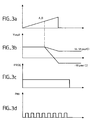
- the circuit detection operation is as follows. As long as the voltage to be monitored, here the supply voltage Vcc which supplies the mirror T3-T4, is less than Vs, the transistors T3 and T4 are blocked. In fact, FIGS. 2a to 2e, when the voltage Vcc, close to 0 Volt, begins to rise, the transistor C2 is conducting, at the limit of the conduction. Indeed it has a negative conduction threshold -Vt. The P-type transistors T3 and T4 are blocked because the voltage Vcc at the start is still less than their conduction threshold on the order of Vt also. Under these conditions the transistor C2 draws the potential of the node B to zero. The potential at node B at zero makes the transistor T5 conductive as soon as Vcc becomes greater than Vt. This means that the signal S at node D then follows the variation of Vcc, Figure 2e.
- Vcc As the voltage, Vcc, applied to the control grid of C1 rises to Vs - Vt, C1 will start to drive. It starts driving as soon as this applied voltage becomes greater than that of its threshold which is equal to Vs - Vt. As soon as C1 drives, T3 and T4 start driving. However, the current supplied by T3 just at this moment is weak because, on the one hand, this current is limited by T1 (at the conduction limit), and on the other hand the current passing through T1 is shared between the passing current by C1 and the current passing through C2.
- Vgs - Vseuil (Vgs is the source gate voltage) of C1 is smaller than the voltage Vgs - Vseuil of C2. This implies that C2 drives more than C1. With the continuation of the increase in Vcc, this situation is reversed: C2 no longer leads and C1 leads more than C2. During the start of conduction of C1, the voltage Vgs - Vseuil of C1 will remain low, which implies that the voltage at node C will then start to rise with Vcc, that at node B also, Figures 2c and 2d.
- the output voltage S goes to zero as soon as the voltage of Vcc exceeds Vs.
- the transistor C1 is subjected to a potential source gate greater than the source gate potential of transistor C2. This is due to the fact that the source grid potential of C2 becomes weaker than -Vt with the increase of the potential of node C.
- This circuit is independent of temperature and manufacturing parameters. This is due to the fact that the threshold voltages change in the same way for the transistors C1 as for the transistor C2.
- a detection voltage equal to (Vs - Vt + ⁇ ) - (-Vt + ⁇ ) ⁇ representing an identical dispersion due to manufacturing, temperature, or voltage.
- the voltage Vs is stored in the circuit during operations to test the operation of this circuit. It is memorized during a programming operation.
- the procedure is preferably as follows. Nodes A and B are connected to pumps of charge P1 and P2 respectively.
- the pump P1 is detailed in the figure.
- This pump P1 has a supply input for a programming potential Vpp and a clock input receiving a phase signal PHI.
- the pump P1 comprises two transistors T10 and T11 of type N in cascade, the drain of the transistor T10 being connected to a programming voltage source Vpp, the source of this transistor T10 being connected to the drain of the transistor T11, the source of the transistor T11 constituting the output of the pump P1 and also being connected to the gate of the transistor T10.
- the gate of transistor T11 is connected to the midpoint between transistors T10 and T11.
- the phase input is connected to this midpoint via a capacitor K1.
- the transistors T3 and T4 respectively decoupling transistors T7 and T8 of type N.
- These transistors T7 and T8 receive on their control grid the supply voltage Vcc. As long as the transistors T7 and T8 have to transmit a positive potential received from the transistors T3 or T4, they conduct. On the other hand, if the potentials at nodes A and B become larger than Vcc, these transistors are blocked since in this case their gates are at the same potential as their source.
- a signal PROG is applied to the control gates of selection transistors respectively T12 of type N and T13 of type P.
- a threshold voltage Vs is imposed on a terminal of the circuit.
- the transistor T12 is connected to this terminal.
- the transistor T13 receives the voltage to be monitored (Vcc) and transmits it on the gate of C1.
- the transistor T12 transmits, when it receives a positive PROG signal on its gate, the threshold voltage value Vs on the control gate of the floating gate transistor C1. Under the same programming conditions, the transistor T13 is blocked.
- the transistor T13 is in short circuit: the transistor C1 monitors the voltage which is applied to it and transmitted by the transistor T13: here in this case the voltage Vcc.
- N type transistors T6 and T9 When programming is put into service, by means of N type transistors T6 and T9 connected in cascade, a derivation to ground of node C.
- the transistor T6 behaves like a diode: preferably its gate is connected to its drain.
- the transistor T9 receives the signal PROG on its control gate.
- the charge pumps P1 and P2 make it possible to apply the voltage Vpp to the nodes A and B during the programming of the device. As soon as PHI starts to oscillate, an output voltage of these charge pumps rises to Vpp plus Vt.
- the advantage of these pumps comes from the fact that, even if one of the nodes A or B were to see its potential collapse, there would not be too much current consumption since only the energy of the PHI signal is consumed.
- each of the transistors C1 or C2 is normally in an erased state, for example with a threshold voltage equal to 6 Volts. They then begin to program themselves, for example first the transistor C2.
- the threshold voltage, FIG. 3b, of this transistor C2 begins to change due to the injection of charges, in practice holes, in its floating gate.
- the threshold voltage of the transistor concerned the transistor C2
- the required threshold that is to say that these holes, by the electric field which they impose, cause the conduction channel to go into conduction
- this transistor begins to drive and programming stops.
- the required threshold is -Vt.
- This required threshold is obtained by connecting the C2 control grid to ground. At the time of conduction the threshold voltage of the transistor then becomes lower than its source gate voltage Vseuil ⁇ Vgs. In the case of C2, this source gate voltage is worth -Vt because T6 mounted as a diode imposes that the potential of the node C is worth Vt, therefore Vgs at the start is worth -Vt.
- the pump P2 does not support any leakage current due to the small amounts of energy transmitted by each pulse of the PHI signal, the voltage on the node concerned, node B, decreases due to conduction and programming stops. It is the same for node A and programming at Vs-Vt of the threshold of transistor C1.
- the device can be replaced by another, a little less precise.
- the transistor C2 can be replaced by a native transistor: a normal transistor, not with gate floating, and whose conduction threshold of the order of 0 Volts is adjusted at the time of the manufacturing steps, by suppressing injection of impurities in its conduction channel.
- this device is less precise because the threshold voltages of the two transistors C1 and C2 then do not change in the same way as a function of the temperature.
- a variation of the order of 0.2 to 0.3 volts can be observed in tolerance of the value of the triggering voltage as a function of the temperature.
- the device described above makes it possible to solve the problems relating to the choice of tripping voltages internal to a circuit.
- this circuit is independent of the parameters of the manufacturing process and of the temperature.
- the proposed solution meets the need for all types of circuits, especially for smart cards. It also has the advantage of having a very low consumption, less than 1 microampere, and therefore also applies to all low consumption circuits.
- the stability of the device depends on the capacity of charge retention on the floating gates of transistors C1 and or C2. In fact, the charges stored on a floating grid of an EEPROM cell can leak slightly. Measurements were made on existing cells. It follows from these measurements that the change in threshold voltage of an EEPROM cell is of the order of 0.2 Volts in 10 years. It is therefore the margin that must be taken in relation to the trigger voltage desired at the time of programming the device.
- the signal S is then used in the circuit for example to neutralize its operation.
Landscapes
- Physics & Mathematics (AREA)
- General Physics & Mathematics (AREA)
- Engineering & Computer Science (AREA)
- Computer Security & Cryptography (AREA)
- Read Only Memory (AREA)
- Electronic Switches (AREA)
- Apparatus Associated With Microorganisms And Enzymes (AREA)
- Control Of Electrical Variables (AREA)
Claims (6)
- Automatische Triggerschaltung, insbesondere eine Nullungsschaltung, mit einem Spannungs-Komparator, der einen ersten Spannungspegel (Vcc) und einen zweiten Spannungspegel empfängt und für eine Änderung eines Ausgangssignals (D) sorgt, wenn eine zu überwachende Spannungsdifferenz einen Schwellenwert (VS) überschreitet, dadurch gekennzeichnet, daß sie umfaßt:- einen Stromspiegel (T3, T4) mit zwei Zweigen, wobei dieser Spiegel zwischen einer Gleichstromzuführung und einer Masse geschaltet ist und jeder Zweig einen Transistor (T3, T4) zur Stromregelung umfaßt und diese beiden Transistoren zusammen als Spiegel montiert sind,- in jedem Zweig, den Regeltransistoren nachgeschaltet, einen Erfassungstransistor (C1, C2), wobei mindestens einer dieser Erfassungstransistoren ein Transistor mit offenem Gitter ist,- wobei die beiden Zweige, den beiden Erfassungstransistoren nachgeschaltet, mit einem Massekopplungstransistor (T1) verbunden sind.
- Schaltung nach Anspruch 1, dadurch gekennzeichnet, daß man bei einem Zweig zwischen dem Regeltransistor und dem Erfassungstransistor mit offenem Gitter einen Entkopplungstransistor (T7, T8) zwischenschaltet, um die Programmierung des Erfassungstransistors mit offenem Gitter zu ermöglichen.
- Schaltung nach Anspruch 1 oder 2, dadurch gekennzeichnet, daß in jedem Zweig ein Erfassungstransistor mit offenem Gitter vorgesehen ist, wobei die Differenz der Leitungsschwellenwerte zwischen den beiden Transistoren mit offenem Gitter (C1, C2) gleich dem Schwellenwert der zu überwachenden Spannungsdifferenz ist, um eine von der Temperatur oder dem Wert einer Speisespannung unabhängige Triggerschaltung zu bilden.
- Schaltung nach einem der Ansprüche 1 bis 3, dadurch gekennzeichnet, daß sie eine Ladungspumpe (P1, P2) mit begrenztem Stromfluß zur Programmierung jedes Erfassungstransistors mit offenem Gitter (C1, C2) aufweist.
- Schaltung nach einem der Ansprüche 1 bis 4, dadurch gekennzeichnet, daß der oder die Transistor/en mit offenem Gitter (C1, C2) vom Typ EEPROM sind.
- Schaltung nach einem der Ansprüche 1 bis 5, dadurch gekennzeichnet, daß sie eine Schaltung (T12, T13, P1, P2) zur Programmierung des Transistors bzw. der Transistoren mit offenem Gitter (C1, C2) aufweist, die umfaßt:- eine Ladungspumpe (P1, P2) zum Anlegen einer Programmierungsspannung,- eine erste Schaltung (T6) zum Anlegen eines ersten Bezugspotentials (Vt) an einen der Transistoren mit offenem Gitter,- eine zweite Schaltung (T13) zum Anlegen eines zweiten Bezugspotentials an einen anderen Transistor mit offenem Gitter, und- eine dritte Schaltung (T9, T12) zur gleichzeitigen Programmierung der beiden Transistoren mit offenem Gitter.
Applications Claiming Priority (2)
| Application Number | Priority Date | Filing Date | Title |
|---|---|---|---|
| FR9303934 | 1993-04-02 | ||
| FR9303934A FR2703526B1 (fr) | 1993-04-02 | 1993-04-02 | Circuit de déclenchement automatique. |
Publications (2)
| Publication Number | Publication Date |
|---|---|
| EP0618657A1 EP0618657A1 (de) | 1994-10-05 |
| EP0618657B1 true EP0618657B1 (de) | 1995-09-27 |
Family
ID=9445708
Family Applications (1)
| Application Number | Title | Priority Date | Filing Date |
|---|---|---|---|
| EP94400736A Expired - Lifetime EP0618657B1 (de) | 1993-04-02 | 1994-04-05 | Automatische Triggerschaltung |
Country Status (6)
| Country | Link |
|---|---|
| US (1) | US5512852A (de) |
| EP (1) | EP0618657B1 (de) |
| JP (1) | JPH0750563A (de) |
| DE (1) | DE69400020T2 (de) |
| ES (1) | ES2078131T3 (de) |
| FR (1) | FR2703526B1 (de) |
Cited By (1)
| Publication number | Priority date | Publication date | Assignee | Title |
|---|---|---|---|---|
| CN111175545A (zh) * | 2019-12-31 | 2020-05-19 | 河北华通燃气设备有限公司 | Ic卡耐久测试工装 |
Families Citing this family (9)
| Publication number | Priority date | Publication date | Assignee | Title |
|---|---|---|---|---|
| FR2739737B1 (fr) * | 1995-10-09 | 1997-11-21 | Inside Technologies | Perfectionnements aux cartes a memoire |
| FR2739706B1 (fr) * | 1995-10-09 | 1997-11-21 | Inside Technologies | Perfectionnements aux cartes a memoire |
| DE69626975T2 (de) * | 1996-09-02 | 2003-11-06 | Siemens Ag | Leseverstärker in Strombetriebsart |
| US5949265A (en) * | 1997-10-31 | 1999-09-07 | International Business Machines Corporation | Soft latch circuit having sharp-cornered hysteresis characteristics |
| JP3139542B2 (ja) | 1998-01-28 | 2001-03-05 | 日本電気株式会社 | 参照電圧発生回路 |
| US6040719A (en) * | 1998-03-17 | 2000-03-21 | Vanguard International Semiconductor Corporation | Input receiver for limiting current during reliability screening |
| JP3416063B2 (ja) * | 1998-10-29 | 2003-06-16 | インターナショナル・ビジネス・マシーンズ・コーポレーション | センスアンプ回路 |
| US6281731B1 (en) | 1999-10-27 | 2001-08-28 | International Business Machines Corporation | Control of hysteresis characteristic within a CMOS differential receiver |
| JP4411199B2 (ja) * | 2002-04-26 | 2010-02-10 | 株式会社ルネサステクノロジ | 半導体装置及びicカード |
Family Cites Families (31)
| Publication number | Priority date | Publication date | Assignee | Title |
|---|---|---|---|---|
| US3984703A (en) * | 1975-06-02 | 1976-10-05 | National Semiconductor Corporation | CMOS Schmitt trigger |
| GB1480984A (en) * | 1975-09-25 | 1977-07-27 | Standard Telephones Cables Ltd | Schmitt trigger circuit |
| JPS56168168A (en) * | 1980-05-29 | 1981-12-24 | Toshiba Corp | Window comparator circuit |
| US4464587A (en) * | 1980-10-14 | 1984-08-07 | Tokyo Shibaura Denki Kabushiki Kaisha | Complementary IGFET Schmitt trigger logic circuit having a variable bias voltage logic gate section |
| US4431927A (en) * | 1981-04-22 | 1984-02-14 | Inmos Corporation | MOS Capacitive bootstrapping trigger circuit for a clock generator |
| JPS5974721A (ja) * | 1982-10-21 | 1984-04-27 | Toshiba Corp | シユミツト・トリガ回路 |
| US4563595A (en) * | 1983-10-27 | 1986-01-07 | National Semiconductor Corporation | CMOS Schmitt trigger circuit for TTL logic levels |
| GB8420651D0 (en) * | 1984-08-14 | 1984-09-19 | British Telecomm | Interface circuit |
| JPS61107594A (ja) * | 1984-10-31 | 1986-05-26 | Toshiba Corp | センス増幅回路 |
| FR2609831B1 (fr) * | 1987-01-16 | 1989-03-31 | Thomson Semiconducteurs | Circuit de lecture pour memoire |
| FR2610134B1 (fr) * | 1987-01-27 | 1989-03-31 | Thomson Semiconducteurs | Circuit de lecture pour memoire |
| FR2613491B1 (fr) * | 1987-04-03 | 1989-07-21 | Thomson Csf | Dispositif de detection du niveau haut d'une tension en technologie mos |
| GB2206010A (en) * | 1987-06-08 | 1988-12-21 | Philips Electronic Associated | Differential amplifier and current sensing circuit including such an amplifier |
| FR2617979B1 (fr) * | 1987-07-10 | 1989-11-10 | Thomson Semiconducteurs | Dispositif de detection de la depassivation d'un circuit integre |
| FR2617976B1 (fr) * | 1987-07-10 | 1989-11-10 | Thomson Semiconducteurs | Detecteur electrique de niveau logique binaire |
| US4859873A (en) * | 1987-07-17 | 1989-08-22 | Western Digital Corporation | CMOS Schmitt trigger with independently biased high/low threshold circuits |
| FR2618579B1 (fr) * | 1987-07-21 | 1989-11-10 | Thomson Semiconducteurs | Circuit integre a memoire comportant un dispositif anti-fraude |
| FR2622019B1 (fr) * | 1987-10-19 | 1990-02-09 | Thomson Semiconducteurs | Dispositif de test structurel d'un circuit integre |
| FR2622038B1 (fr) * | 1987-10-19 | 1990-01-19 | Thomson Semiconducteurs | Procede de programmation des cellules memoire d'une memoire et circuit pour la mise en oeuvre de ce procede |
| FR2623018B1 (fr) * | 1987-11-06 | 1990-02-09 | Thomson Semiconducteurs | Circuit integre protege contre les decharges electrostatiques avec seuil de protection variable |
| FR2623016B1 (fr) * | 1987-11-06 | 1991-06-14 | Thomson Semiconducteurs | Dispositif de fusion d'un fusible dans un circuit integre de type cmos |
| US4904884A (en) * | 1988-04-21 | 1990-02-27 | Western Digital Corporation | Schmitt trigger adapted to interface between different transistor architectures |
| FR2642543B1 (fr) * | 1989-01-27 | 1991-04-05 | Gemplus Card Int | Dispositif de securite pour circuit integre |
| US5148395A (en) * | 1989-04-26 | 1992-09-15 | Exar Corporation | Dual eeprom cell with current mirror differential read |
| FR2649817B1 (fr) * | 1989-07-13 | 1993-12-24 | Gemplus Card International | Carte a microcircuit protegee contre l'intrusion |
| JP3142542B2 (ja) * | 1990-06-13 | 2001-03-07 | 沖電気工業株式会社 | 電圧測定回路 |
| FR2667714A1 (fr) * | 1990-10-09 | 1992-04-10 | Gemplus Card Int | Procede pour repartir la memoire d'un circuit integre entre plusieurs applications. |
| FR2673016B1 (fr) * | 1991-02-19 | 1993-04-30 | Gemplus Card Int | Procede de protection d'un circuit integre contre les utilisations frauduleuses. |
| FR2673316B1 (fr) * | 1991-02-22 | 1994-12-23 | Gemplus Card Int | Dispositif d'adressage sequentiel d'une memoire, notamment pour carte a memoire. |
| FR2681180B1 (fr) * | 1991-09-05 | 1996-10-25 | Gemplus Card Int | Circuit de regulation de tension de programmation, pour memoires programmables. |
| FR2686997B1 (fr) * | 1992-01-30 | 1994-04-01 | Gemplus Card International | Carte a puce a deux contacts et procede de communication avec un lecteur de carte. |
-
1993
- 1993-04-02 FR FR9303934A patent/FR2703526B1/fr not_active Expired - Fee Related
-
1994
- 1994-04-01 US US08/222,260 patent/US5512852A/en not_active Expired - Lifetime
- 1994-04-04 JP JP6089157A patent/JPH0750563A/ja not_active Ceased
- 1994-04-05 ES ES94400736T patent/ES2078131T3/es not_active Expired - Lifetime
- 1994-04-05 DE DE69400020T patent/DE69400020T2/de not_active Expired - Fee Related
- 1994-04-05 EP EP94400736A patent/EP0618657B1/de not_active Expired - Lifetime
Cited By (2)
| Publication number | Priority date | Publication date | Assignee | Title |
|---|---|---|---|---|
| CN111175545A (zh) * | 2019-12-31 | 2020-05-19 | 河北华通燃气设备有限公司 | Ic卡耐久测试工装 |
| CN111175545B (zh) * | 2019-12-31 | 2022-02-11 | 河北华通燃气设备有限公司 | Ic卡耐久测试工装 |
Also Published As
| Publication number | Publication date |
|---|---|
| EP0618657A1 (de) | 1994-10-05 |
| US5512852A (en) | 1996-04-30 |
| ES2078131T3 (es) | 1995-12-01 |
| FR2703526A1 (fr) | 1994-10-07 |
| DE69400020T2 (de) | 1996-03-07 |
| DE69400020D1 (de) | 1995-11-02 |
| FR2703526B1 (fr) | 1995-05-19 |
| JPH0750563A (ja) | 1995-02-21 |
Similar Documents
| Publication | Publication Date | Title |
|---|---|---|
| EP0568439B1 (de) | Detektionsverfahren und -schaltung für Stromverluste in einer Bitleitung | |
| EP1079525B1 (de) | System zur Steuerung eines Zweirichtungs-Schalters mit zwei Transistoren | |
| EP0300885B1 (de) | Integrierte Speicherschaltung, die eine Antibetrugseinrichtung einschliesst | |
| EP0618657B1 (de) | Automatische Triggerschaltung | |
| US6815685B2 (en) | Photodetector and method for detecting radiation | |
| FR2660457A1 (fr) | Circuit de protection contre l'effacement et la programmation d'une memoire remanente. | |
| EP2302341A2 (de) | Detektionsschaltung mit verbessertem Blendschutz | |
| FR2601832A1 (fr) | Circuit de retablissement du fonctionnement stable d'un circuit logique, notamment d'un microprocesseur | |
| FR2688952A1 (fr) | Dispositif de generation de tension de reference. | |
| US7683653B2 (en) | Process and circuit for improving the life duration of field-effect transistors | |
| FR2978244A1 (fr) | Capteur de mesure de rayonnement ultraviolet | |
| CA2692300A1 (fr) | Procede et systeme de gestion de coupures d'alimentation electrique a bord d'un aeronef | |
| EP1672795A1 (de) | Vorrichtung zur Reinitialisierung eines integrierten Schaltkreises anhand der Detektion eines Spannungsabfalls der Stromversorgung und elektrische Schaltung hierfür | |
| FR3050307A1 (fr) | Circuit amplificateur de lecture perfectionne pour un dispositif de memoire, en particulier un dispositif de memoire non volatile | |
| EP0700141A1 (de) | Temperaturdetektor auf einer integrierten Schaltung | |
| EP0750244B1 (de) | Ladungspumpe-Generator-Schaltkreis für negative Spannung | |
| EP0902437B1 (de) | Hochspannungsgeneratorschaltung zum Programmieren oder Löschen eines Speichers | |
| EP3147909B1 (de) | Verfahren zur kontrolle eines schreibzyklus eines speichers vom typ eeprom, und entsprechende vorrichtung | |
| FR2680596A1 (fr) | Appareil pour tester automatiquement un mode surcharge d'un dispositif de memoire a semiconducteurs. | |
| EP0581639B1 (de) | Schutzschaltung gegen Stromunterbrechungen für eine integrierte Schaltung | |
| FR2822309A1 (fr) | Circuit de translation de signaux de commutation | |
| EP0323367B1 (de) | Einschalt-Rücksetzschaltung für eine integrierte Schaltung in MOS-Technik | |
| FR2757712A1 (fr) | Dispositif de controle de mise sous tension ou hors tension d'un circuit integre | |
| FR3050308A1 (fr) | Procede et dispositif de commande d'au moins un circuit de pompe de charge | |
| FR3104751A1 (fr) | Procédé de lissage d’un courant consommé par un circuit intégré et dispositif correspondant |
Legal Events
| Date | Code | Title | Description |
|---|---|---|---|
| PUAI | Public reference made under article 153(3) epc to a published international application that has entered the european phase |
Free format text: ORIGINAL CODE: 0009012 |
|
| AK | Designated contracting states |
Kind code of ref document: A1 Designated state(s): DE ES GB IT NL |
|
| 17P | Request for examination filed |
Effective date: 19940816 |
|
| 17Q | First examination report despatched |
Effective date: 19950201 |
|
| GRAA | (expected) grant |
Free format text: ORIGINAL CODE: 0009210 |
|
| AK | Designated contracting states |
Kind code of ref document: B1 Designated state(s): DE ES GB IT NL |
|
| REF | Corresponds to: |
Ref document number: 69400020 Country of ref document: DE Date of ref document: 19951102 |
|
| GBT | Gb: translation of ep patent filed (gb section 77(6)(a)/1977) |
Effective date: 19951014 |
|
| ITF | It: translation for a ep patent filed | ||
| REG | Reference to a national code |
Ref country code: ES Ref legal event code: FG2A Ref document number: 2078131 Country of ref document: ES Kind code of ref document: T3 |
|
| PLBE | No opposition filed within time limit |
Free format text: ORIGINAL CODE: 0009261 |
|
| STAA | Information on the status of an ep patent application or granted ep patent |
Free format text: STATUS: NO OPPOSITION FILED WITHIN TIME LIMIT |
|
| 26N | No opposition filed | ||
| REG | Reference to a national code |
Ref country code: GB Ref legal event code: IF02 |
|
| PGFP | Annual fee paid to national office [announced via postgrant information from national office to epo] |
Ref country code: GB Payment date: 20080326 Year of fee payment: 15 |
|
| PGFP | Annual fee paid to national office [announced via postgrant information from national office to epo] |
Ref country code: ES Payment date: 20080404 Year of fee payment: 15 Ref country code: DE Payment date: 20080408 Year of fee payment: 15 |
|
| PGFP | Annual fee paid to national office [announced via postgrant information from national office to epo] |
Ref country code: IT Payment date: 20080409 Year of fee payment: 15 |
|
| PGFP | Annual fee paid to national office [announced via postgrant information from national office to epo] |
Ref country code: NL Payment date: 20080326 Year of fee payment: 15 |
|
| GBPC | Gb: european patent ceased through non-payment of renewal fee |
Effective date: 20090405 |
|
| NLV4 | Nl: lapsed or anulled due to non-payment of the annual fee |
Effective date: 20091101 |
|
| PG25 | Lapsed in a contracting state [announced via postgrant information from national office to epo] |
Ref country code: DE Free format text: LAPSE BECAUSE OF NON-PAYMENT OF DUE FEES Effective date: 20091103 |
|
| PG25 | Lapsed in a contracting state [announced via postgrant information from national office to epo] |
Ref country code: NL Free format text: LAPSE BECAUSE OF NON-PAYMENT OF DUE FEES Effective date: 20091101 |
|
| PG25 | Lapsed in a contracting state [announced via postgrant information from national office to epo] |
Ref country code: GB Free format text: LAPSE BECAUSE OF NON-PAYMENT OF DUE FEES Effective date: 20090405 |
|
| REG | Reference to a national code |
Ref country code: ES Ref legal event code: FD2A Effective date: 20090406 |
|
| PG25 | Lapsed in a contracting state [announced via postgrant information from national office to epo] |
Ref country code: ES Free format text: LAPSE BECAUSE OF NON-PAYMENT OF DUE FEES Effective date: 20090406 |
|
| PG25 | Lapsed in a contracting state [announced via postgrant information from national office to epo] |
Ref country code: IT Free format text: LAPSE BECAUSE OF NON-PAYMENT OF DUE FEES Effective date: 20090405 |