EP1079525B1 - System zur Steuerung eines Zweirichtungs-Schalters mit zwei Transistoren - Google Patents
System zur Steuerung eines Zweirichtungs-Schalters mit zwei Transistoren Download PDFInfo
- Publication number
- EP1079525B1 EP1079525B1 EP99117676A EP99117676A EP1079525B1 EP 1079525 B1 EP1079525 B1 EP 1079525B1 EP 99117676 A EP99117676 A EP 99117676A EP 99117676 A EP99117676 A EP 99117676A EP 1079525 B1 EP1079525 B1 EP 1079525B1
- Authority
- EP
- European Patent Office
- Prior art keywords
- transistors
- switch
- transistor
- state
- power
- Prior art date
- Legal status (The legal status is an assumption and is not a legal conclusion. Google has not performed a legal analysis and makes no representation as to the accuracy of the status listed.)
- Expired - Lifetime
Links
Images


Classifications
-
- H—ELECTRICITY
- H03—ELECTRONIC CIRCUITRY
- H03K—PULSE TECHNIQUE
- H03K17/00—Electronic switching or gating, i.e. not by contact-making and –breaking
- H03K17/04—Modifications for accelerating switching
- H03K17/041—Modifications for accelerating switching without feedback from the output circuit to the control circuit
- H03K17/0412—Modifications for accelerating switching without feedback from the output circuit to the control circuit by measures taken in the control circuit
- H03K17/04123—Modifications for accelerating switching without feedback from the output circuit to the control circuit by measures taken in the control circuit in field-effect transistor switches
-
- H—ELECTRICITY
- H03—ELECTRONIC CIRCUITRY
- H03K—PULSE TECHNIQUE
- H03K17/00—Electronic switching or gating, i.e. not by contact-making and –breaking
- H03K17/51—Electronic switching or gating, i.e. not by contact-making and –breaking characterised by the components used
- H03K17/56—Electronic switching or gating, i.e. not by contact-making and –breaking characterised by the components used by the use, as active elements, of semiconductor devices
- H03K17/687—Electronic switching or gating, i.e. not by contact-making and –breaking characterised by the components used by the use, as active elements, of semiconductor devices the devices being field-effect transistors
- H03K17/6871—Electronic switching or gating, i.e. not by contact-making and –breaking characterised by the components used by the use, as active elements, of semiconductor devices the devices being field-effect transistors the output circuit comprising more than one controlled field-effect transistor
- H03K17/6874—Electronic switching or gating, i.e. not by contact-making and –breaking characterised by the components used by the use, as active elements, of semiconductor devices the devices being field-effect transistors the output circuit comprising more than one controlled field-effect transistor in a symmetrical configuration
Definitions
- the present invention relates to a control system of a bidirectional switch for current control circuits, including current control circuits adapted to control the charging and discharging of rechargeable batteries. More particularly, the present invention relates to a control system of a bidirectional switch formed of a pair of power MOSFET transistors connected in anti-series, that is to say source source or drain drain.
- Circuits for controlling the bi-directional flow of a current are used in many applications. Such circuits are used in particular to control the charging and discharging of rechargeable batteries (lithium batteries, lithium-ion batteries, etc.) supplying power to portable devices of various types (telephones, laptops, timepieces , etc.).
- rechargeable batteries lithium batteries, lithium-ion batteries, etc.
- Rechargeable batteries of this type are known to require protection against improper operating conditions (overcharging or overcharging of the battery, excessive charging or discharging currents, too high operating temperature, etc.) that may occur when charger or a charger is connected to the battery or during a short circuit of the battery terminals. This protection is necessary to ensure that the performance of the battery is not degraded.
- These current control circuits thus typically comprise current interruption means placed in series in the path of the battery current and responding to signals indicative of improper operating conditions, so as to interrupt the continuation of the charge or the discharge of the battery or, in general, to interrupt the flow of a current in the battery that could have a detrimental effect on the performance of the latter.
- These current interruption means are commonly formed of switches made by means of power MOSFET transistors and controlled by circuits monitoring the charge or discharge level of the battery, the value of the current flowing through it or the temperature drums.
- these means of interruption are formed of a switch comprising a pair of power MOSFET transistors connected anti-series, that is to say source source or alternatively drain to drain.
- the Figures 1a to 1c illustrate three examples of such a bidirectional switch with two transistors.
- the figure 1a illustrates a pair of source-source connected N-MOSFET transistors
- the figure 1b illustrates a pair of N-MOSFETs connected drain-to-drain
- the figure 1c illustrates a pair of P-MOSFET transistors connected source to source.
- a fourth solution not illustrated here, is to connect a pair of P-MOSFET drain-drain transistors.
- This type of switch is commonly referred to as a "bidirectional switch" because it allows the blocking and the flow of a current in two directions.
- both transistors are in the "ON" state and current can flow in both directions between terminals X and Y through the switch.
- either one of the transistors is set to "OFF” to block the flow of current in the battery.
- the current can however flow in the opposite direction through a parasitic diode (“body diode”) formed between the drain and the source of each power MOSFET transistor, this parasitic diode being due to the fact that the substrate ( “body”) and the source of the power transistor are set to the same potential.
- body diode parasitic diode
- Each transistor thus makes it possible to ensure the unidirectional blocking of the current while allowing the passage of a current of opposite direction through its parasitic diode.
- one of the transistors used in a circuit for controlling the charge and discharge of rechargeable batteries, one of the transistors makes it possible to ensure the interruption of the charge current of the battery, while the other transistor ensures the interruption of the current discharge in the opposite direction.
- An object of the present invention is thus to provide a control system of a bidirectional switch with two transistors in particular to meet the two opposite objectives mentioned above.
- the subject of the present invention is a control system for a bidirectional switch with two transistors, the characteristics of which are set forth in claim 1.
- the present invention further relates to a method of controlling a bidirectional switch with two transistors, the characteristics of which are set forth in claim 5.
- the bidirectional switch is composed of two power transistors mounted anti-series and that only one of the transistors is set to the "OFF" state when it is desired interrupt the flow of current through the battery, the other transistor always remains in the "ON" state.
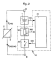
- FIG. 1 schematically illustrated a protection circuit 10 of a rechargeable battery 1.
- the battery 1 and the protection circuit 10 form an assembly comprising two terminals a and b between which a load 2 or a charger 3 can be connected.
- the protection circuit which may more generally be referred to as the current control circuit 10, comprises means for interrupting the current, formed by a bidirectional switch 20, and possibly current measuring means 30 arranged in series with the battery 1 between the terminals a and b of the set.
- a discharge current I DISCHG flows from the positive terminal of the battery 1 via the load 2 and the bidirectional switch 20 to the terminal negative battery 1.
- a charger 3 is connected between the terminals a and b of the set, a charging current I CHG then flows in the opposite direction to the discharge current I DISCHG .
- the measuring means 30 can be made in the form of a measurement resistor providing a potential drop representative of the current flowing through it.
- the bidirectional switch 20 can however also form the measuring means 30. In this case, the voltage across the bidirectional switch 20 is used to evaluate the value of the charging current I CHG or discharge I DISCHG through the battery 1 .
- the current control circuit 10 further comprises detection and control means 40 coupled to the battery 1 and, if appropriate, to the measuring means 30.
- the detection and control means 40 receive from the battery 1 and the measuring means 30 of the detection signals 100 and 300 respectively representative of the level of charge of the battery 1 and the value of the current flowing through the battery 1.
- the detection and control means 40 supply one or more control signals 400 to the bidirectional switch 20. will not describe in detail here how these detection and control means 40 are made.
- these means typically comprise, on the one hand, detection and comparison means making it possible in particular to compare the voltage across the terminals of the battery at different levels of reference voltage and to provide, in response, logic level activation signals, and, secondly, control means responsive to these activation signals and forming strictly speaking the control system. bidirectional switch control 20.
- FIG. 3 illustrates the block diagram of the control system of a bidirectional switch with two power MOSFET transistors according to the present invention.
- the bidirectional switch 20 illustrated in this figure is formed in this example of a pair of N-MOSFET power transistors 210 and 220 connected source to source.
- Each of the power transistors 210 and 220 includes a parasitic diode ("body diode") 215, 225 formed between the drain and the source of the transistors in parallel with the channel.
- the drains of the power transistors 210 and 220 are connected in accordance with what has been previously described so that the bidirectional switch is arranged in the path of the current whose circulation must, if necessary, be interrupted.
- a first current namely a charge current I CHG
- a second current in the opposite direction to the first current namely a discharge current I DISCHG
- the gates 211 and 221 of the power transistors 210 and 220 are respectively connected to control means 50 delivering first and second gate voltage V GATE_CHG and V GATE_DISCHG to the gates 211 and 221, respectively, of the power transistors 210 and 220.
- V GATE_CHG and V GATE_DISCHG When either of these gate voltages V GATE_CHG and V GATE_DISCHG is substantially equal to the voltage present at the node formed by the sources of transistors 210 and 220, here the ground, the corresponding power transistor is made non-conductive , that is, set to the "OFF" state.
- the gate voltage is brought to a level such that the voltage between the gate and the source of the transistor is greater than the threshold voltage (typically from 0.7 to 2.5 volts) of this transistor.
- the gate voltages V GATE_CHG and V GATE_DISCHG are preferably brought to levels such that the gate-source voltage of each of the transistors is substantially greater than the threshold voltage (typically 5 to 15 volts above the threshold voltage).
- the control means 50 preferably comprise two charge pumps 510 and 520 respectively connected to the gates 211 and 221 of the power MOSFET transistors 210 and 220. These charge pumps are widely used and make it possible to produce a higher output voltage. high as their input voltage. Typically, these charge pumps are adapted to double or triple their input voltage. It should be noted that this type of device is also known under the name voltage doubler or voltage tripler. In the application example used here, it will be mentioned that the charge pumps are thus typically adapted to triple an input voltage V dd defined as the voltage of the rechargeable battery.
- two blocking switches SW CHG and SW DISCHG respectively arranged in first and second branches 500a and 500b make it possible to connect each of the grids 211 and 221 to ground in order to put, if necessary, the power transistor corresponding to the state "OFF".
- the charge pumps 510 and 520 are deactivated when the corresponding transistor must be in the "OFF" state.
- the SW CHG and SW DISCHG blocking switches can thus be integrated directly into the charge pumps 510 and 520.
- control means 50 furthermore comprise a coupling means connected between the grids 211 and 221 of the power MOSFET transistors 210 and 220.
- This coupling means can easily be implemented in the form of a coupling switch SW CPL adapted to connect the gates 211 and 221 of the power transistors as shown in FIG. figure 3 .
- this coupling switch SW CPL is adapted to at least temporarily couple the gates 211 and 221 of the power transistors 210 and 220 when one or the other of these transistors, which had previously been set to state "OFF" to interrupt the flow of a current, must be reset to "ON".
- the coupling switch SW CPL forming the coupling means can be controlled by a control signal formed by a logic combination of the activation signals. controlling respectively the switches SW CHG and SW DISCHG .
- CONTCHG and CONTDISCHG activation signals are used to respectively control the switches SW CHG and SW DISCHG , these activation signals being in the "high" logic state when the power transistors have to be set in the "ON" state
- the control signal of the coupling switch SW CPL can be defined as the logical AND combination of these activation signals CONTCHG and CONTDISCHG.
- the switches SW CHG , SW DISCHG and SW CPL must be adapted to switch between relatively high voltages (of the order of the gate voltage applied to the power transistors 210 and 220, ie more than ten volts ). It is conceivable to make these switches by means of MOSFET transistors adapted to withstand such switching voltages.
- the response time of the coupling switch SW CPL is decisive for the switching duration at the "ON" state of the bidirectional switch 20. It is therefore preferable to minimize the switching time at the switch. "ON" state of the coupling switch SW CPL , that is to say use low voltage MOSFET transistors with a low gate capacitance.
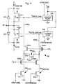
- the figure 4 illustrates an embodiment of a control system of a bidirectional switch with two transistors made in low voltage CMOS technology. Identical reference numerals have been used in this figure to designate the elements common to this embodiment and to the schematic diagram of the figure 3 .
- the bidirectional switch 20 formed of the pair of power N-MOSFET transistors 210 and 220 is thus controlled by the control means 50 including the charge pumps 510 and 520 supply respectively V gate voltages GATE_CHG and V GATE_DISCHG equivalent in this embodiment, three times the input voltage V dd provided by the battery.
- the first branch 500a comprising the blocking switch SW CHG makes it possible to pull the gate 211 of the power MOSFET transistor 210 to ground in order to put it in the "OFF" state.
- the second branch 500b including the blocking switch SW DISCHG makes it possible to pull the gate 221 of the power MOSFET transistor 220 to ground in order to put the latter in the "OFF” state.
- the SW CHG and SW DISCHG blocking switches are formed of MOSFETs 511 and 512, respectively, one of whose terminals is connected to ground. The gates of these MOSFETs 511 and 512 are respectively controlled by the inverted CONTCHG and CONTDISCHG activation signals.
- the branches 500a and 500b furthermore comprise each of the first and second protection transistors 501a and 502a, respectively 501b and 502b, connected in series between the gate of the corresponding power MOSFET transistor and the corresponding blocking switch, namely respectively between the gate 211 of the power transistor 210 and the switch SW CHG on the one hand, and between the gate 221 of the power transistor 220 and the switch SW DISCHG on the other hand.
- the gates of the first protection transistors 501a and 501b are connected together and controlled by a first control voltage V 1 .
- the gates of the second protection transistors 502a and 502b are connected together and controlled by a second control voltage V 2 .
- the coupling switch SW CPL formed in this example of a coupling MOSFET transistor 510, is connected between the connection node of the first and second protection transistors 501a and 502a of the first branch 500a, and the connection node of the first and second protection transistors 501b and 502b of the second branch 500b.
- the gate of the coupling transistor 510 forming the coupling switch is controlled by a control voltage V CPL representative of the activation signals CONTCHG and CONTDISCHG of the blocking switches SW CHG and SW DISCHG .
- this control voltage V CPL is substantially 0 so as to decouple the gates 211 and 221 from the power transistors 210 and 220 when one of the activation signals CONTCHG and CONTDISCHG signals that one of these Power transistors must be set to the "OFF" state.
- the control voltage V CPL of the gate of the coupling transistor 510 is brought to a substantially equal value. at the gate voltage of the power transistors 210 and 220.
- the first gates of protection transistors 501a and 501b and the gates of the second protection transistors 502a and 502b are controlled in the following manner.
- the first control voltage V 1 of the first protection transistors 501a and 501b is brought to a value substantially equal to the gate voltage of the power transistors 210 and 220, that is to say about three times the input voltage V dd .
- the second control voltage V 2 of the second protection transistors 502a and 502b is brought to a value substantially equal to twice the input voltage V dd .
- the first control voltage V 1 is reduced to a voltage substantially equal to twice the input voltage V dd
- the second control voltage V 2 is in turn reduced to a voltage substantially equal to the input voltage V dd .
- This method of controlling the gates of the protection switches 501a, 502a, 501b and 502b thus ensures that none of the transistors sees too high a voltage at its terminals, which could lead to a breakdown of the latter.
- FIGs 5a to 5d illustrate four diagrams of evolution of the various control voltages of the control system of the figure 4 in response to the CONTCHG and CONTDISCHG activation signals, to demonstrate the beneficial effects of the present invention.
- the figure 5a thus presents a first diagram in which the CONTCHG and CONTDISCHG activation signals are illustrated.
- the figure 5b presents a second diagram in which are illustrated a first curve representative of the evolution of twice the voltage V dd supplied by the battery and a second curve b representative of the evolution of the second control voltage V 2 of the second transistors of protection 502a and 502b of the figure 4 .
- the figure 5c presents a third diagram in which is illustrated a third curve c representative of the evolution of the first control voltage V 1 of the first protection transistors 501a and 501b of the figure 4 , and a fourth curve d representative of the evolution of the control voltage V CPL of the coupling transistor 510.
- figure 5d for its part presents a fourth diagram in which are illustrated fifth and sixth curves e and f respectively representative of the evolution of the gate voltages V GATE_CHG and V GATE_DISCHG of the power MOSFET transistors 210 and 220.
- the gate voltage V GATE_DISCHG of the power MOSFET transistor 220 is substantially equal to 0 so that this transistor is set to the "OFF" state in order to interrupt any further discharge of the battery.
- the power MOSFET 210 is maintained in the "ON” state by applying the gate voltage V GATE_CHG equivalent to about three times the voltage V dd .
- the first and second control voltages V 1 and V 2 are worth in this case, as already mentioned, about two and respectively once the voltage V dd .
- the control voltage V CPL of the coupling transistor 510 is in turn maintained substantially at 0 so that the gates of the power MOSFET transistors 210 and 220 of the figure 4 are kept uncoupled.
- the control voltage V CPL of the coupling transistor 510 changes to about three times the voltage V dd so that the gates of the power MOSFET transistors 210 and 220 are coupled.
- the first and second control voltages V 1 and V 2 of the protection transistors are respectively three and twice the voltage V dd .
- the charges present on the gate of the power MOSFET transistor 210 remained in the "ON" state are shared with the power MOSFET transistor 220.
- the gate of the power MOSFET transistor 220 is thus very quickly charged to a level sufficient to make it conductive by the transfer of a portion of the transistor charges Power MOSFET 210 remained in the "ON" state. Since the conduction threshold of the power MOSFET transistors is approximately 1 volt, it can thus be seen that the power MOSFET transistor 220 is turned on “ON” virtually instantaneously.
- the load of the gates of the power MOSFET transistors represented by the curves e and f of the figure 5d follows a normal evolution.
- control system according to the present invention can be subject to many modifications and / or improvements without departing from the scope of the claims.
- those skilled in the art are perfectly able to modify the control system according to the present invention to adapt it to lower or higher control voltages depending on the application.
- the control system of a bidirectional switch according to the present invention is also applicable to circuits other than battery protection circuits which have been used here as examples.
Landscapes
- Electronic Switches (AREA)
- Charge And Discharge Circuits For Batteries Or The Like (AREA)
- Use Of Switch Circuits For Exchanges And Methods Of Control Of Multiplex Exchanges (AREA)
Claims (6)
- System zum Steuern eines bidirektionalen Unterbrechers (20), der aus einem Paar von Leistungs-MOSFET-Transistoren (210, 220), die in Antireihe, Source mit Source oder Drain mit Drain, geschaltet sind, gebildet ist, wobei dieses Steuersystem Steuermittel (50) umfasst, die dazu vorgesehen sind, den Durchschaltzustand der Leistungstransistoren (210, 220), die mit den Steuermitteln verbunden sind, zu steuern, wobei der eine oder der andere dieser Leistungstransistoren durch die Steuermittel in den "AUS"-Zustand versetzt werden kann, um die Unterbrechung eines Stroms (ICHG, IDISCHG) durch den Unterbrecher (20) sicherzustellen, wobei die Steuermittel außerdem ein Kopplungsmittel (SWCPL, 510) umfassen, das dazu vorgesehen ist, wenigstens vorübergehend das Gate (211; 221) eines Unterbrechertransistors im "EIN"-Zustand mit dem Gate (221, 211) eines Unterbrechertransistors im "AUS"-Zustand zu verbinden, wenn der Unterbrecher (20) ausgelöst wird, oder dazu vorgesehen ist, die Gates der Unterbrechertransistoren ständig zu verbinden, wenn sie in den "EIN"-Zustand gesteuert sind, wobei die Steuermittel (50) außerdem einen ersten und einen zweiten Zweig (500a, 500b) umfassen, die dazu vorgesehen sind, jeweils mit den Gates (211, 221) der Leistungstransistoren (210, 220) des Unterbrechers verbunden zu werden, und jeweils einen Sperrunterbrecher (SWCHG, SWDISCHG; 511, 512) umfassen, der ermöglicht, den entsprechenden Leistungstransistor (210, 220) in den "AUS"-Zustand zu versetzen, dadurch gekennzeichnet, dass jeder der Zweige (500a, 500b) außerdem einen ersten Schutztransistor (501a, 501b) und einen zweiten Schutztransistor (502a, 502b) umfasst, die zwischen dem Gate (211, 221) des entsprechenden Leistungstransistors (210, 220) und dem Sperrunterbrecher (SWCHG, SWDISCHG; 511, 512) in Reihe geschaltet sind, wobei das Kopplungsmittel (SWCPL, 510) zwischen dem Verbindungsknoten des ersten und des zweiten Schutztransistors (501a, 502a) des ersten Zweigs (500a) und dem Verbindungsknoten des ersten und des zweiten Schutztransistors (501 b, 502b) des zweiten Zweigs (500b) geschaltet ist.
- Steuersystem nach Anspruch 1, dadurch gekennzeichnet, dass die Steuermittel (50) zwei Ladungspumpen (510, 520) umfassen, die jeweils dazu vorgesehen sind, mit dem Gate (211, 221) des entsprechenden Leistungstransistors (210, 220) verbunden zu werden.
- Steuersystem nach Anspruch 1, dadurch gekennzeichnet, dass die Sperrunterbrecher (SWCHG, SWDISCHG; 511, 512) MOSFET-Transistoren sind.
- Steuersystem nach einem der vorhergehenden Ansprüche, dadurch gekennzeichnet, dass das Kopplungsmittel ein MOSFET-Transistor ist.
- Verfahren zum Steuern eines bidirektionalen Unterbrechers (20), der aus einem Paar von Leistungs-MOSFET-Transistoren (210, 220), die in Antireihe, Source mit Source oder Drain mit Drain, geschaltet sind und durch Steuermittel (50) eines Steuersystems nach einem der vorhergehenden Ansprüche gesteuert werden, gebildet ist, wobei der eine oder der andere der Leistungstransistoren (210, 220) in den "AUS"-Zustand versetzt werden kann, um die Unterbrechung eines Stroms (ICHG, IDISCHG) durch den Unterbrecher (20) sicherzustellen, wobei in dem Verfahren bei der Auslösung des Unterbrechers (20) das Gate (211; 221) des Transistors im "EIN"-Zustand wenigstens vorübergehend mit dem Gate (221; 211) des Transistors im "AUS"-Zustand verbunden wird.
- Steuerverfahren nach Anspruch 5, bei dem die Gates (211, 221) der Leistungstransistoren (210, 220) ständig verbunden sind, wenn jene im "EIN"-Zustand sind.
Applications Claiming Priority (2)
| Application Number | Priority Date | Filing Date | Title |
|---|---|---|---|
| CH153099 | 1999-08-20 | ||
| CH153099 | 1999-08-20 |
Publications (2)
| Publication Number | Publication Date |
|---|---|
| EP1079525A1 EP1079525A1 (de) | 2001-02-28 |
| EP1079525B1 true EP1079525B1 (de) | 2008-09-10 |
Family
ID=4212606
Family Applications (1)
| Application Number | Title | Priority Date | Filing Date |
|---|---|---|---|
| EP99117676A Expired - Lifetime EP1079525B1 (de) | 1999-08-20 | 1999-09-08 | System zur Steuerung eines Zweirichtungs-Schalters mit zwei Transistoren |
Country Status (8)
| Country | Link |
|---|---|
| US (1) | US6259306B1 (de) |
| EP (1) | EP1079525B1 (de) |
| JP (1) | JP2001111403A (de) |
| CN (1) | CN1285657A (de) |
| AT (1) | ATE408272T1 (de) |
| DE (1) | DE69939535D1 (de) |
| SG (1) | SG83808A1 (de) |
| TW (1) | TW465184B (de) |
Families Citing this family (45)
| Publication number | Priority date | Publication date | Assignee | Title |
|---|---|---|---|---|
| US6501193B1 (en) * | 2001-09-07 | 2002-12-31 | Power-One, Inc. | Power converter having regulated dual outputs |
| US7102253B2 (en) * | 2001-12-31 | 2006-09-05 | Lewis James M | MOSFET based, high voltage, electronic relays for AC power switching and inductive loads |
| US7439636B2 (en) * | 2001-12-31 | 2008-10-21 | Lewis James M | Driver system for MOSFET based, high voltage electronic relays for AC power switching and inductive loads |
| US7230354B2 (en) * | 2001-12-31 | 2007-06-12 | Lewis James M | Driver system for MOSFET based, high voltage, electronic relays for AC power switching and inductive loads |
| US6683393B2 (en) | 2001-12-31 | 2004-01-27 | James M. Lewis | MOSFET based, high voltage, electronic relays for AC power switching and inductive loads |
| US7183672B2 (en) * | 2001-12-31 | 2007-02-27 | Lewis James M | MOSFET based, high voltage, electronic relays for AC power switching and inductive loads |
| US7199640B2 (en) | 2002-10-29 | 2007-04-03 | Dxp B.V. | Bi-directional double NMOS switch |
| US7372685B2 (en) * | 2003-05-20 | 2008-05-13 | On Semiconductor | Multi-fault protected high side switch with current sense |
| EP1498998A1 (de) * | 2003-07-16 | 2005-01-19 | Dialog Semiconductor GmbH | Schutzschalter mit Sperrspannungsschutz |
| US20050162870A1 (en) * | 2004-01-23 | 2005-07-28 | Hirst B. M. | Power converter |
| US20050162139A1 (en) * | 2004-01-23 | 2005-07-28 | Mark Hirst | Alternating current switching circuit |
| US8253394B2 (en) | 2004-02-17 | 2012-08-28 | Hewlett-Packard Development Company, L.P. | Snubber circuit |
| HUP0400419A2 (hu) * | 2004-02-16 | 2005-12-28 | András Fazakas | Kis veszteségű, elektronikusan vezérelhető váltakozóáramú félvezetős kapcsolóeszköz |
| JP2006033723A (ja) * | 2004-07-21 | 2006-02-02 | Sharp Corp | 電力制御用光結合素子およびこの電力制御用光結合素子を用いた電子機器 |
| JP2006147700A (ja) * | 2004-11-17 | 2006-06-08 | Sanyo Electric Co Ltd | 半導体装置 |
| JP2006311507A (ja) * | 2005-03-28 | 2006-11-09 | Matsushita Electric Ind Co Ltd | 電源スイッチ回路 |
| US7457092B2 (en) * | 2005-12-07 | 2008-11-25 | Alpha & Omega Semiconductor, Lld. | Current limited bilateral MOSFET switch with reduced switch resistance and lower manufacturing cost |
| US8937504B2 (en) * | 2010-04-12 | 2015-01-20 | Sapiens Steering Brain Stimulation B.V. | Control circuitry and method for controlling a bi-directional switch system, a bi-directional switch, a switching matrix and a medical stimulator |
| CN102005734B (zh) * | 2010-10-20 | 2013-09-18 | 无锡中星微电子有限公司 | 电池保护集成电路及系统 |
| FR2967837A1 (fr) * | 2010-11-23 | 2012-05-25 | Peugeot Citroen Automobiles Sa | Systeme d'alimentation en energie electrique d'organes consommateurs equipant un vehicule automobile |
| US8941264B2 (en) * | 2011-06-20 | 2015-01-27 | Bae Systems Information And Electronic Systems Integration Inc. | Apparatus for bi-directional power switching in low voltage vehicle power distribution systems |
| WO2013066867A2 (en) | 2011-10-31 | 2013-05-10 | Cobasys, Llc | Parallel configuration of series cells with semiconductor switching |
| US9166419B2 (en) | 2011-10-31 | 2015-10-20 | Robert Bosch Gmbh | Intelligent charging and discharging system for parallel configuration of series cells with semiconductor switching |
| JP5529178B2 (ja) * | 2012-01-19 | 2014-06-25 | 旭化成エレクトロニクス株式会社 | 電源接続装置 |
| JP5710516B2 (ja) * | 2012-02-08 | 2015-04-30 | オムロンオートモーティブエレクトロニクス株式会社 | 電源装置 |
| US8933533B2 (en) * | 2012-07-05 | 2015-01-13 | Infineon Technologies Austria Ag | Solid-state bidirectional switch having a first and a second power-FET |
| US9498601B2 (en) | 2013-03-14 | 2016-11-22 | Hansen Medical, Inc. | Catheter tension sensing |
| KR102141822B1 (ko) * | 2013-06-26 | 2020-08-06 | 삼성전자주식회사 | 충전시간을 단축하기 위한 제어회로 및 그 구동방법 |
| US9680300B2 (en) * | 2013-12-13 | 2017-06-13 | Keithley Instruments, Llc | Hot switch protection circuit |
| JP6309855B2 (ja) * | 2014-07-31 | 2018-04-11 | 株式会社東芝 | レギュレータ回路 |
| KR101599733B1 (ko) * | 2014-11-12 | 2016-03-04 | 한국기초과학지원연구원 | 플라즈마를 이용한 액체 처리 장치 |
| US9627962B2 (en) * | 2015-03-09 | 2017-04-18 | Texas Instruments Incorporated | Fast blocking switch |
| JP6601026B2 (ja) * | 2015-07-09 | 2019-11-06 | 株式会社Ihi | 半導体スイッチ回路及び半導体リレー回路 |
| CN105356421A (zh) * | 2015-11-27 | 2016-02-24 | 上海中兴派能能源科技有限公司 | 一种锂电池组充放电保护电路 |
| CN105429222A (zh) * | 2015-12-15 | 2016-03-23 | 成都默一科技有限公司 | 一种采用单端口的充电及放电装置 |
| CN106059549A (zh) * | 2016-05-31 | 2016-10-26 | 天津市三源电力设备制造有限公司 | 一种基于pmos的新型双向模拟开关电路 |
| JP6745478B2 (ja) * | 2016-06-30 | 2020-08-26 | パナソニックIpマネジメント株式会社 | 保護回路及び配線器具 |
| CN106602667A (zh) * | 2017-01-20 | 2017-04-26 | 浙江大学昆山创新中心 | 一种移动机器人自动充电保护系统及保护方法 |
| CN106992569A (zh) * | 2017-05-05 | 2017-07-28 | 江苏金帆电源科技有限公司 | 一种充放电控制电路 |
| DE102017012069A1 (de) | 2017-12-29 | 2019-07-04 | Thomas Kliem | Elektronische Schaltungsanordnung |
| EP3509131A1 (de) * | 2018-01-08 | 2019-07-10 | Samsung SDI Co., Ltd. | Schaltbares batteriemodul |
| US10432184B1 (en) * | 2018-08-09 | 2019-10-01 | Texas Instruments Incorporated | Channel switchover power multiplexer circuits, and methods of operating the same |
| CN109617184A (zh) * | 2018-12-29 | 2019-04-12 | 维沃移动通信有限公司 | 一种升压电路和终端 |
| JP7265468B2 (ja) * | 2019-12-17 | 2023-04-26 | 株式会社東芝 | 半導体集積回路、及び半導体集積回路の制御方法 |
| CN114982133A (zh) * | 2020-12-28 | 2022-08-30 | 深圳市速腾聚创科技有限公司 | 激光接收电路和激光雷达 |
Family Cites Families (12)
| Publication number | Priority date | Publication date | Assignee | Title |
|---|---|---|---|---|
| FR2635930B1 (fr) * | 1988-08-31 | 1990-11-23 | Sgs Thomson Microelectronics | Commutateur bidirectionnel monolithique a transistors mos de puissance |
| US5138186A (en) * | 1990-07-13 | 1992-08-11 | Illinois Tool Works Inc. | Solid state switch with last state memory |
| JP3136677B2 (ja) * | 1991-07-31 | 2001-02-19 | ソニー株式会社 | 2次電池の過充電及び過放電防止回路 |
| DE69433808T2 (de) | 1993-11-30 | 2005-06-09 | Siliconix Inc., Santa Clara | Vielfach-Spannungsversorgung und Verfahren zur Auswahl einer Spannungsquelle aus einer Vielzahl von Spannungsquellen |
| US5574633A (en) * | 1994-02-23 | 1996-11-12 | At&T Global Information Solubions Company | Multi-phase charge sharing method and apparatus |
| US5610495A (en) | 1994-06-20 | 1997-03-11 | Motorola, Inc. | Circuit and method of monitoring battery cells |
| US5808502A (en) * | 1995-06-05 | 1998-09-15 | Hewlett-Packard Co. | Parallel micro-relay bus switch for computer network communication with reduced crosstalk and low on-resistance using charge pumps |
| DE19548612B4 (de) * | 1995-12-23 | 2005-10-06 | Robert Bosch Gmbh | Mehrkreisiges Fahrzeugbordnetz mit einem elektronischen Analogschalter |
| US5789902A (en) | 1996-02-22 | 1998-08-04 | Hitachi Metals, Ltd. | Bi-direction current control circuit for monitoring charge/discharge of a battery |
| US5764032A (en) * | 1997-03-06 | 1998-06-09 | Maxim Integrated Products, Inc. | Multiple battery switchover circuits |
| US5909103A (en) | 1997-07-24 | 1999-06-01 | Siliconix Incorporated | Safety switch for lithium ion battery |
| US6163199A (en) * | 1999-01-29 | 2000-12-19 | Fairchild Semiconductor Corp. | Overvoltage/undervoltage tolerant transfer gate |
-
1999
- 1999-09-08 AT AT99117676T patent/ATE408272T1/de active
- 1999-09-08 DE DE69939535T patent/DE69939535D1/de not_active Expired - Lifetime
- 1999-09-08 EP EP99117676A patent/EP1079525B1/de not_active Expired - Lifetime
-
2000
- 2000-08-12 SG SG200004422A patent/SG83808A1/en unknown
- 2000-08-14 TW TW089116368A patent/TW465184B/zh not_active IP Right Cessation
- 2000-08-14 US US09/638,558 patent/US6259306B1/en not_active Expired - Lifetime
- 2000-08-21 CN CN00124095A patent/CN1285657A/zh active Pending
- 2000-08-21 JP JP2000250132A patent/JP2001111403A/ja active Pending
Also Published As
| Publication number | Publication date |
|---|---|
| JP2001111403A (ja) | 2001-04-20 |
| ATE408272T1 (de) | 2008-09-15 |
| US6259306B1 (en) | 2001-07-10 |
| DE69939535D1 (de) | 2008-10-23 |
| TW465184B (en) | 2001-11-21 |
| SG83808A1 (en) | 2001-10-16 |
| CN1285657A (zh) | 2001-02-28 |
| EP1079525A1 (de) | 2001-02-28 |
Similar Documents
| Publication | Publication Date | Title |
|---|---|---|
| EP1079525B1 (de) | System zur Steuerung eines Zweirichtungs-Schalters mit zwei Transistoren | |
| EP1936541B1 (de) | Ein/aus Batterieladegerät mit Versorgungsschutzschaltung für eine monolithische integrierte Schaltung die verwendet die Energie von der Antenne | |
| EP1081572B1 (de) | Versorgungsschaltung mit Spannungswähler | |
| FR2722031A1 (fr) | Dispositif regulateur pour batterie d'accumulateurs electriques | |
| FR2731110A1 (fr) | Dispositif de protection de piles rechargeables et transistor mosfet equipant ce dispositif | |
| EP1977514B1 (de) | Steuerung eines mos-transistors | |
| EP1825557B1 (de) | Verfahren zur steuerung einer wiederaufladbaren batterie und wiederaufladbare batterie zur ausführung des verfahrens | |
| FR2970123A1 (fr) | Circuit de protection d'une batterie en couches minces | |
| EP2184855B1 (de) | Integrierte Schaltung mit leckstromabhängiger Basisvorspannung eines Leistungstransistors | |
| EP0323367B1 (de) | Einschalt-Rücksetzschaltung für eine integrierte Schaltung in MOS-Technik | |
| FR2724501A1 (fr) | Appareil egaliseur de charge pour des batteries connectees en serie | |
| FR2874467A1 (fr) | Circuit pour un generateur d'eeprom haute tension | |
| EP3401647A1 (de) | Messsystem für den leistungspegel einer umweltenergiequelle | |
| FR2879321A1 (fr) | Circuit de pilotage de bus | |
| EP1942577A1 (de) | Integrierter Schaltkreis mit im Ruhemodus reduziertem Stromverbrauch | |
| EP0180487A1 (de) | Leistungsschaltung und diese enthaltende Auslösevorrichtung | |
| FR2549999A1 (fr) | Cellule de memoire du type ram comprenant un element de memoire non volatil electriquement programmable | |
| EP1047174B1 (de) | Batterieschutzschaltung | |
| EP3185389B1 (de) | Vorrichtung und elektrisches gerät zur erzeugung einer elektrischen spannung für eine informationsbearbeitungseinheit, und entsprechendes elektronisches system zur informationsbearbeitung | |
| FR3055752B1 (fr) | Circuit de transmission d'energie electrique | |
| EP0164770B1 (de) | Statisches Relais für niedrige Gleichstromspannung | |
| EP2174200A1 (de) | Schnell reagierender stromversorgungsschalter und mit einem derartigen schalter ausgerüstetes stromversorgungsnetz | |
| FR3106447A1 (fr) | Element de stockage d’energie electrique et alimentation sauvegardee associee | |
| FR2731851A1 (fr) | Pont redresseur a chute de tension reduite | |
| FR2843245A1 (fr) | Dispositif et procede de protection d'un composant electronique contre des surcharges dommageables |
Legal Events
| Date | Code | Title | Description |
|---|---|---|---|
| PUAI | Public reference made under article 153(3) epc to a published international application that has entered the european phase |
Free format text: ORIGINAL CODE: 0009012 |
|
| AK | Designated contracting states |
Kind code of ref document: A1 Designated state(s): AT BE CH CY DE DK ES FI FR GB GR IE IT LI LU MC NL PT SE |
|
| AX | Request for extension of the european patent |
Free format text: AL;LT;LV;MK;RO;SI |
|
| 17P | Request for examination filed |
Effective date: 20010828 |
|
| AKX | Designation fees paid |
Free format text: AT BE CH CY DE DK ES FI FR GB GR IE IT LI LU MC NL PT SE |
|
| 17Q | First examination report despatched |
Effective date: 20061205 |
|
| GRAP | Despatch of communication of intention to grant a patent |
Free format text: ORIGINAL CODE: EPIDOSNIGR1 |
|
| GRAS | Grant fee paid |
Free format text: ORIGINAL CODE: EPIDOSNIGR3 |
|
| GRAA | (expected) grant |
Free format text: ORIGINAL CODE: 0009210 |
|
| AK | Designated contracting states |
Kind code of ref document: B1 Designated state(s): AT BE CH CY DE DK ES FI FR GB GR IE IT LI LU MC NL PT SE |
|
| REG | Reference to a national code |
Ref country code: GB Ref legal event code: FG4D Free format text: NOT ENGLISH |
|
| REG | Reference to a national code |
Ref country code: CH Ref legal event code: EP |
|
| REG | Reference to a national code |
Ref country code: IE Ref legal event code: FG4D Free format text: LANGUAGE OF EP DOCUMENT: FRENCH |
|
| REF | Corresponds to: |
Ref document number: 69939535 Country of ref document: DE Date of ref document: 20081023 Kind code of ref document: P |
|
| REG | Reference to a national code |
Ref country code: CH Ref legal event code: NV Representative=s name: ICB INGENIEURS CONSEILS EN BREVETS SA |
|
| PG25 | Lapsed in a contracting state [announced via postgrant information from national office to epo] |
Ref country code: FI Free format text: LAPSE BECAUSE OF FAILURE TO SUBMIT A TRANSLATION OF THE DESCRIPTION OR TO PAY THE FEE WITHIN THE PRESCRIBED TIME-LIMIT Effective date: 20080910 |
|
| NLV1 | Nl: lapsed or annulled due to failure to fulfill the requirements of art. 29p and 29m of the patents act | ||
| REG | Reference to a national code |
Ref country code: IE Ref legal event code: FD4D |
|
| PG25 | Lapsed in a contracting state [announced via postgrant information from national office to epo] |
Ref country code: IE Free format text: LAPSE BECAUSE OF FAILURE TO SUBMIT A TRANSLATION OF THE DESCRIPTION OR TO PAY THE FEE WITHIN THE PRESCRIBED TIME-LIMIT Effective date: 20080910 Ref country code: ES Free format text: LAPSE BECAUSE OF FAILURE TO SUBMIT A TRANSLATION OF THE DESCRIPTION OR TO PAY THE FEE WITHIN THE PRESCRIBED TIME-LIMIT Effective date: 20081221 |
|
| PG25 | Lapsed in a contracting state [announced via postgrant information from national office to epo] |
Ref country code: PT Free format text: LAPSE BECAUSE OF FAILURE TO SUBMIT A TRANSLATION OF THE DESCRIPTION OR TO PAY THE FEE WITHIN THE PRESCRIBED TIME-LIMIT Effective date: 20090210 Ref country code: NL Free format text: LAPSE BECAUSE OF FAILURE TO SUBMIT A TRANSLATION OF THE DESCRIPTION OR TO PAY THE FEE WITHIN THE PRESCRIBED TIME-LIMIT Effective date: 20080910 |
|
| PLBE | No opposition filed within time limit |
Free format text: ORIGINAL CODE: 0009261 |
|
| STAA | Information on the status of an ep patent application or granted ep patent |
Free format text: STATUS: NO OPPOSITION FILED WITHIN TIME LIMIT |
|
| PG25 | Lapsed in a contracting state [announced via postgrant information from national office to epo] |
Ref country code: DK Free format text: LAPSE BECAUSE OF FAILURE TO SUBMIT A TRANSLATION OF THE DESCRIPTION OR TO PAY THE FEE WITHIN THE PRESCRIBED TIME-LIMIT Effective date: 20080910 |
|
| 26N | No opposition filed |
Effective date: 20090611 |
|
| PG25 | Lapsed in a contracting state [announced via postgrant information from national office to epo] |
Ref country code: IT Free format text: LAPSE BECAUSE OF FAILURE TO SUBMIT A TRANSLATION OF THE DESCRIPTION OR TO PAY THE FEE WITHIN THE PRESCRIBED TIME-LIMIT Effective date: 20080910 |
|
| PG25 | Lapsed in a contracting state [announced via postgrant information from national office to epo] |
Ref country code: SE Free format text: LAPSE BECAUSE OF FAILURE TO SUBMIT A TRANSLATION OF THE DESCRIPTION OR TO PAY THE FEE WITHIN THE PRESCRIBED TIME-LIMIT Effective date: 20081210 |
|
| BERE | Be: lapsed |
Owner name: EM MICROELECTRONIC-MARIN SA Effective date: 20090930 |
|
| PG25 | Lapsed in a contracting state [announced via postgrant information from national office to epo] |
Ref country code: MC Free format text: LAPSE BECAUSE OF NON-PAYMENT OF DUE FEES Effective date: 20090930 |
|
| GBPC | Gb: european patent ceased through non-payment of renewal fee |
Effective date: 20090908 |
|
| PG25 | Lapsed in a contracting state [announced via postgrant information from national office to epo] |
Ref country code: BE Free format text: LAPSE BECAUSE OF NON-PAYMENT OF DUE FEES Effective date: 20090930 |
|
| PG25 | Lapsed in a contracting state [announced via postgrant information from national office to epo] |
Ref country code: GR Free format text: LAPSE BECAUSE OF FAILURE TO SUBMIT A TRANSLATION OF THE DESCRIPTION OR TO PAY THE FEE WITHIN THE PRESCRIBED TIME-LIMIT Effective date: 20081211 |
|
| PG25 | Lapsed in a contracting state [announced via postgrant information from national office to epo] |
Ref country code: GB Free format text: LAPSE BECAUSE OF NON-PAYMENT OF DUE FEES Effective date: 20090908 |
|
| PG25 | Lapsed in a contracting state [announced via postgrant information from national office to epo] |
Ref country code: LU Free format text: LAPSE BECAUSE OF NON-PAYMENT OF DUE FEES Effective date: 20090908 |
|
| PG25 | Lapsed in a contracting state [announced via postgrant information from national office to epo] |
Ref country code: CY Free format text: LAPSE BECAUSE OF FAILURE TO SUBMIT A TRANSLATION OF THE DESCRIPTION OR TO PAY THE FEE WITHIN THE PRESCRIBED TIME-LIMIT Effective date: 20080910 |
|
| PGFP | Annual fee paid to national office [announced via postgrant information from national office to epo] |
Ref country code: AT Payment date: 20130821 Year of fee payment: 15 |
|
| REG | Reference to a national code |
Ref country code: AT Ref legal event code: MM01 Ref document number: 408272 Country of ref document: AT Kind code of ref document: T Effective date: 20140908 |
|
| REG | Reference to a national code |
Ref country code: FR Ref legal event code: PLFP Year of fee payment: 17 |
|
| PG25 | Lapsed in a contracting state [announced via postgrant information from national office to epo] |
Ref country code: AT Free format text: LAPSE BECAUSE OF NON-PAYMENT OF DUE FEES Effective date: 20140908 |
|
| REG | Reference to a national code |
Ref country code: FR Ref legal event code: PLFP Year of fee payment: 18 |
|
| REG | Reference to a national code |
Ref country code: FR Ref legal event code: PLFP Year of fee payment: 19 |
|
| REG | Reference to a national code |
Ref country code: FR Ref legal event code: PLFP Year of fee payment: 20 |
|
| PGFP | Annual fee paid to national office [announced via postgrant information from national office to epo] |
Ref country code: FR Payment date: 20180822 Year of fee payment: 20 Ref country code: DE Payment date: 20180821 Year of fee payment: 20 |
|
| PGFP | Annual fee paid to national office [announced via postgrant information from national office to epo] |
Ref country code: CH Payment date: 20180828 Year of fee payment: 20 |
|
| REG | Reference to a national code |
Ref country code: DE Ref legal event code: R071 Ref document number: 69939535 Country of ref document: DE |
|
| REG | Reference to a national code |
Ref country code: CH Ref legal event code: PL |