EP0617439A2 - Dünnschichtkondensator und Herstellungsverfahren - Google Patents
Dünnschichtkondensator und Herstellungsverfahren Download PDFInfo
- Publication number
- EP0617439A2 EP0617439A2 EP94104693A EP94104693A EP0617439A2 EP 0617439 A2 EP0617439 A2 EP 0617439A2 EP 94104693 A EP94104693 A EP 94104693A EP 94104693 A EP94104693 A EP 94104693A EP 0617439 A2 EP0617439 A2 EP 0617439A2
- Authority
- EP
- European Patent Office
- Prior art keywords
- thin layer
- layer
- face
- oxide thin
- oriented
- Prior art date
- Legal status (The legal status is an assumption and is not a legal conclusion. Google has not performed a legal analysis and makes no representation as to the accuracy of the status listed.)
- Granted
Links
- 239000003990 capacitor Substances 0.000 title claims abstract description 107
- 239000010409 thin film Substances 0.000 title claims abstract description 69
- 238000004519 manufacturing process Methods 0.000 title claims description 9
- 239000000758 substrate Substances 0.000 claims abstract description 96
- FAPWRFPIFSIZLT-UHFFFAOYSA-M Sodium chloride Chemical compound [Na+].[Cl-] FAPWRFPIFSIZLT-UHFFFAOYSA-M 0.000 claims abstract description 94
- 238000000034 method Methods 0.000 claims abstract description 62
- 239000011780 sodium chloride Substances 0.000 claims abstract description 47
- 229910052596 spinel Inorganic materials 0.000 claims abstract description 39
- 239000011029 spinel Substances 0.000 claims abstract description 39
- 229910052751 metal Inorganic materials 0.000 claims abstract description 35
- 239000002184 metal Substances 0.000 claims abstract description 35
- 238000004544 sputter deposition Methods 0.000 claims abstract description 32
- 238000000623 plasma-assisted chemical vapour deposition Methods 0.000 claims abstract description 29
- 238000005229 chemical vapour deposition Methods 0.000 claims abstract description 18
- 238000001771 vacuum deposition Methods 0.000 claims abstract description 10
- 229910010252 TiO3 Inorganic materials 0.000 claims description 78
- XEEYBQQBJWHFJM-UHFFFAOYSA-N Iron Chemical compound [Fe] XEEYBQQBJWHFJM-UHFFFAOYSA-N 0.000 claims description 35
- 239000011777 magnesium Substances 0.000 claims description 19
- CPLXHLVBOLITMK-UHFFFAOYSA-N magnesium oxide Inorganic materials [Mg]=O CPLXHLVBOLITMK-UHFFFAOYSA-N 0.000 claims description 6
- 239000000395 magnesium oxide Substances 0.000 claims description 5
- 229910052782 aluminium Inorganic materials 0.000 claims description 4
- XAGFODPZIPBFFR-UHFFFAOYSA-N aluminium Chemical compound [Al] XAGFODPZIPBFFR-UHFFFAOYSA-N 0.000 claims description 4
- 229910017052 cobalt Inorganic materials 0.000 claims description 4
- 239000010941 cobalt Substances 0.000 claims description 4
- GUTLYIVDDKVIGB-UHFFFAOYSA-N cobalt atom Chemical compound [Co] GUTLYIVDDKVIGB-UHFFFAOYSA-N 0.000 claims description 4
- 229910000428 cobalt oxide Inorganic materials 0.000 claims description 4
- IVMYJDGYRUAWML-UHFFFAOYSA-N cobalt(ii) oxide Chemical compound [Co]=O IVMYJDGYRUAWML-UHFFFAOYSA-N 0.000 claims description 4
- 229910052742 iron Inorganic materials 0.000 claims description 4
- AXZKOIWUVFPNLO-UHFFFAOYSA-N magnesium;oxygen(2-) Chemical compound [O-2].[Mg+2] AXZKOIWUVFPNLO-UHFFFAOYSA-N 0.000 claims description 4
- 229910000480 nickel oxide Inorganic materials 0.000 claims description 4
- GNRSAWUEBMWBQH-UHFFFAOYSA-N oxonickel Chemical compound [Ni]=O GNRSAWUEBMWBQH-UHFFFAOYSA-N 0.000 claims description 4
- BASFCYQUMIYNBI-UHFFFAOYSA-N platinum Chemical compound [Pt] BASFCYQUMIYNBI-UHFFFAOYSA-N 0.000 abstract description 107
- 229910052697 platinum Inorganic materials 0.000 abstract description 32
- 230000015572 biosynthetic process Effects 0.000 abstract description 5
- 238000010030 laminating Methods 0.000 abstract 1
- PXHVJJICTQNCMI-UHFFFAOYSA-N Nickel Chemical compound [Ni] PXHVJJICTQNCMI-UHFFFAOYSA-N 0.000 description 44
- 239000010408 film Substances 0.000 description 43
- XKRFYHLGVUSROY-UHFFFAOYSA-N Argon Chemical compound [Ar] XKRFYHLGVUSROY-UHFFFAOYSA-N 0.000 description 22
- 239000000203 mixture Substances 0.000 description 20
- VXUYXOFXAQZZMF-UHFFFAOYSA-N titanium(IV) isopropoxide Chemical compound CC(C)O[Ti](OC(C)C)(OC(C)C)OC(C)C VXUYXOFXAQZZMF-UHFFFAOYSA-N 0.000 description 20
- 239000010936 titanium Substances 0.000 description 14
- 239000013078 crystal Substances 0.000 description 13
- 238000010438 heat treatment Methods 0.000 description 13
- BMGNSKKZFQMGDH-FDGPNNRMSA-L nickel(2+);(z)-4-oxopent-2-en-2-olate Chemical class [Ni+2].C\C([O-])=C\C(C)=O.C\C([O-])=C\C(C)=O BMGNSKKZFQMGDH-FDGPNNRMSA-L 0.000 description 13
- 239000012159 carrier gas Substances 0.000 description 12
- 239000007789 gas Substances 0.000 description 12
- 229910052786 argon Inorganic materials 0.000 description 11
- QVGXLLKOCUKJST-UHFFFAOYSA-N atomic oxygen Chemical compound [O] QVGXLLKOCUKJST-UHFFFAOYSA-N 0.000 description 11
- 239000000463 material Substances 0.000 description 11
- 239000001301 oxygen Substances 0.000 description 11
- 229910052760 oxygen Inorganic materials 0.000 description 11
- 229910002714 Ba0.5Sr0.5 Inorganic materials 0.000 description 10
- KDLHZDBZIXYQEI-UHFFFAOYSA-N Palladium Chemical compound [Pd] KDLHZDBZIXYQEI-UHFFFAOYSA-N 0.000 description 10
- XBNIACLTQUNWQC-UHFFFAOYSA-N barium;2,2,6,6-tetramethylheptane-3,5-dione Chemical compound [Ba].CC(C)(C)C(=O)CC(=O)C(C)(C)C XBNIACLTQUNWQC-UHFFFAOYSA-N 0.000 description 10
- DPWYUDXLMNQOOU-UHFFFAOYSA-N strontium;2,2,6,6-tetramethylheptane-3,5-dione Chemical compound [Sr].CC(C)(C)C(=O)CC(=O)C(C)(C)C DPWYUDXLMNQOOU-UHFFFAOYSA-N 0.000 description 10
- CUJRVFIICFDLGR-UHFFFAOYSA-N acetylacetonate Chemical compound CC(=O)[CH-]C(C)=O CUJRVFIICFDLGR-UHFFFAOYSA-N 0.000 description 9
- 239000000919 ceramic Substances 0.000 description 8
- 229910052759 nickel Inorganic materials 0.000 description 8
- 229910002113 barium titanate Inorganic materials 0.000 description 7
- LZKLAOYSENRNKR-LNTINUHCSA-N iron;(z)-4-oxoniumylidenepent-2-en-2-olate Chemical compound [Fe].C\C(O)=C\C(C)=O.C\C(O)=C\C(C)=O.C\C(O)=C\C(C)=O LZKLAOYSENRNKR-LNTINUHCSA-N 0.000 description 7
- 229910001316 Ag alloy Inorganic materials 0.000 description 5
- RYGMFSIKBFXOCR-UHFFFAOYSA-N Copper Chemical compound [Cu] RYGMFSIKBFXOCR-UHFFFAOYSA-N 0.000 description 5
- 229910001252 Pd alloy Inorganic materials 0.000 description 5
- BQCADISMDOOEFD-UHFFFAOYSA-N Silver Chemical compound [Ag] BQCADISMDOOEFD-UHFFFAOYSA-N 0.000 description 5
- 238000002441 X-ray diffraction Methods 0.000 description 5
- JRPBQTZRNDNNOP-UHFFFAOYSA-N barium titanate Chemical compound [Ba+2].[Ba+2].[O-][Ti]([O-])([O-])[O-] JRPBQTZRNDNNOP-UHFFFAOYSA-N 0.000 description 5
- 230000015556 catabolic process Effects 0.000 description 5
- 229910052802 copper Inorganic materials 0.000 description 5
- 239000010949 copper Substances 0.000 description 5
- 238000009413 insulation Methods 0.000 description 5
- 229910052763 palladium Inorganic materials 0.000 description 5
- 239000002245 particle Substances 0.000 description 5
- 125000002572 propoxy group Chemical group [*]OC([H])([H])C(C([H])([H])[H])([H])[H] 0.000 description 5
- 238000002128 reflection high energy electron diffraction Methods 0.000 description 5
- 239000004332 silver Substances 0.000 description 5
- 238000004458 analytical method Methods 0.000 description 4
- 239000003989 dielectric material Substances 0.000 description 4
- 238000001755 magnetron sputter deposition Methods 0.000 description 4
- 150000002739 metals Chemical class 0.000 description 4
- VEALVRVVWBQVSL-UHFFFAOYSA-N strontium titanate Chemical compound [Sr+2].[O-][Ti]([O-])=O VEALVRVVWBQVSL-UHFFFAOYSA-N 0.000 description 4
- QTBSBXVTEAMEQO-UHFFFAOYSA-M Acetate Chemical compound CC([O-])=O QTBSBXVTEAMEQO-UHFFFAOYSA-M 0.000 description 3
- 238000004453 electron probe microanalysis Methods 0.000 description 3
- 239000000523 sample Substances 0.000 description 3
- 238000001816 cooling Methods 0.000 description 2
- -1 Pb(Mg1/3 Chemical class 0.000 description 1
- 239000000654 additive Substances 0.000 description 1
- 230000000996 additive effect Effects 0.000 description 1
- 229910052788 barium Inorganic materials 0.000 description 1
- DSAJWYNOEDNPEQ-UHFFFAOYSA-N barium atom Chemical compound [Ba] DSAJWYNOEDNPEQ-UHFFFAOYSA-N 0.000 description 1
- 150000001875 compounds Chemical class 0.000 description 1
- 230000000694 effects Effects 0.000 description 1
- 230000002708 enhancing effect Effects 0.000 description 1
- 239000003822 epoxy resin Substances 0.000 description 1
- 238000002474 experimental method Methods 0.000 description 1
- 229920000647 polyepoxide Polymers 0.000 description 1
- 239000004065 semiconductor Substances 0.000 description 1
- 238000003980 solgel method Methods 0.000 description 1
Images


Classifications
-
- H—ELECTRICITY
- H01—ELECTRIC ELEMENTS
- H01G—CAPACITORS; CAPACITORS, RECTIFIERS, DETECTORS, SWITCHING DEVICES, LIGHT-SENSITIVE OR TEMPERATURE-SENSITIVE DEVICES OF THE ELECTROLYTIC TYPE
- H01G4/00—Fixed capacitors; Processes of their manufacture
- H01G4/002—Details
- H01G4/018—Dielectrics
- H01G4/20—Dielectrics using combinations of dielectrics from more than one of groups H01G4/02 - H01G4/06
-
- H—ELECTRICITY
- H01—ELECTRIC ELEMENTS
- H01L—SEMICONDUCTOR DEVICES NOT COVERED BY CLASS H10
- H01L2224/00—Indexing scheme for arrangements for connecting or disconnecting semiconductor or solid-state bodies and methods related thereto as covered by H01L24/00
- H01L2224/01—Means for bonding being attached to, or being formed on, the surface to be connected, e.g. chip-to-package, die-attach, "first-level" interconnects; Manufacturing methods related thereto
- H01L2224/42—Wire connectors; Manufacturing methods related thereto
- H01L2224/47—Structure, shape, material or disposition of the wire connectors after the connecting process
- H01L2224/49—Structure, shape, material or disposition of the wire connectors after the connecting process of a plurality of wire connectors
- H01L2224/491—Disposition
- H01L2224/4918—Disposition being disposed on at least two different sides of the body, e.g. dual array
-
- H—ELECTRICITY
- H01—ELECTRIC ELEMENTS
- H01L—SEMICONDUCTOR DEVICES NOT COVERED BY CLASS H10
- H01L2924/00—Indexing scheme for arrangements or methods for connecting or disconnecting semiconductor or solid-state bodies as covered by H01L24/00
- H01L2924/15—Details of package parts other than the semiconductor or other solid state devices to be connected
- H01L2924/181—Encapsulation
Definitions
- the invention relates to a thin film capacitor and a method of manufacturing the same.
- Barium titanate (BaTiO3) ceramics having a perovskite crystal structure have been widely used as capacitor materials and the like, since they have high resistivities and superior dielectric properties.
- Strontium titanate (SrTiO3) becomes cubical at about a temperature higher than 110K, and is paraelectric. Ceramics mainly made from strontium titanate have lower dielectric constants than do the barium titanate ceramics. However, the strontium titanate ceramics have better temperature characteristics and less dielectric loss than do the barium titanate ceramics.
- the curie points of ceramics can be shifted by employing an additive such as barium, lead or the like, thus providing paraelectric ceramics with a high dielectric constant at room temperature.
- These ceramics have been widely used for high frequency range and high voltage capacitors.
- complex perovskite compounds such as Pb(Mg 1/3 , Nb 2/3 )O3 and Pb ⁇ (Mg 1/3 , Nb 2/3 ) 1-Y Ti Y ⁇ O3 have higher dielectric constants and better direct current biases than do barium titanate dielectrics, they are used for small multilayer capacitors with high capacitance and the like.
- oxide materials having a perovskite structure and large dielectric constants such as barium titanate dielectric materials, strontium titanate dielectric materials, Pb ⁇ (Mg 1/3 , Nb 2/3 ) 1-Y Ti Y ⁇ O3 dielectric materials and the like has been actively carried out in order to manufacture small high-volume capacitors.
- a sputtering method As a method of forming thin layers, a sputtering method has been conventionally applied. (For example, the method is disclosed in K. Iijima et al., J. Appl. Phys., vol. 60, No.1, pp.361-367 (1986).) However, this method is slow in forming layers ( ⁇ 10nm/min), requires expensive monocrystal substrates such as MgO and is poor in controlling the compositions of layers.
- a sol-gel method which has been intensively researched recently, on the other hand, is excellent in controlling the compositions of layers and suitable for forming multicomponent thin layers.
- this method provides layers with poor quality and coverage over uneven surfaces so that it cannot be applied as an industrial manufacturing technique.
- a CVD (chemical vapor deposition) method is excellent in controlling the compositions of layers, and can form layers on substrates having large surface areas.
- the method also has a good property of covering uneven surfaces. Therefore, this method can be applied as a method of forming perovskite dielectric thin layers.
- the CVD method can form layers at high speed. However, the speed of forming a dielectric thin layer by the CVD method is still about 3 ⁇ m/h.
- Layers should be formed at a higher speed so that a thin film capacitor can be manufactured at lower cost.
- a dielectric thin layer is directly formed on a metal electrode substrate or a metal thin layer by a sputtering method or a CVD method, a layer with poor crystallinities (initial growth layer) is formed in the early stages of film growth. Due to the formation of the initial growth layer, the electric characteristics of the thin film capacitor are lowered as the capacity of the capacitor is increased by thinning the dielectric thin layer.
- a plasma-enhanced CVD method making use of plasma activity and CVD reaction can form layers at low temperature and high speed by dissolving and enhancing source materials with an active plasma.
- the plasma-enhanced CVD method forms a layer with poor crystallinity (initial growth layer) in the early stages of film growth when a dielectric layer is directly formed on a metal electrode substrate or a metal thin layer.
- a thin film capacitor comprising: a lower electrode directly or indirectly formed on a metal substrate (electrode) or a nonelectrode substrate; a dielectric thin layer directly or indirectly formed on the surface of the lower electrode; and an upper electrode formed on the dielectric thin layer.
- the indirect formation of a lower electrode on a substrate, or a dielectric thin layer on the lower electrode is due to the formation of at least one intervening oxide thin layer in between; conversely, direct formation allows for no intervening layers.
- the dielectric thin layer is a perovskite type dielectric thin layer oriented to (100) face. Anywhere below the dielectric thin layer, at least one of an NaCl type oxide thin layer oriented to (100) face and a spinel type oxide thin layer oriented to (100) face may additionally be formed.
- the perovskite type oxide, NaCl type oxide and spinel type oxide is also called perovskite oxide, NaCl oxide and spinel oxide.
- orientations of the perovskite dielectric thin layer, the NaCl oxide thin layer and the spinel oxide thin layer to (100) face refer to the growth of the (100) face of a perovskite, NaCl and spinel crystal structure in a parallel orientation to the substrate surface.
- At least one of the NaCl oxide thin layer oriented to (100) face and the spinel oxide thin layer oriented to (100) face is formed between the lower electrode and the perovskite dielectric thin layer.
- the perovskite dielectric thin layer is (Ba 1-X Sr X )TiO3 (0 ⁇ X ⁇ 1.0) or Pb ⁇ (Mg 1/3 , Nb 2/3 ) 1-Y Ti Y ⁇ O3 (0 ⁇ Y ⁇ 1.0).
- the NaCl oxide thin layer is a magnesium oxide thin layer, a cobalt oxide thin layer, and/or a nickel oxide thin layer.
- the spinel oxide thin layer is an oxide thin layer mainly comprising at least one of the elements iron, cobalt and aluminum.
- the thin film capacitor has the lower electrode directly formed on the nonelectrode substrate, the NaCl oxide thin layer oriented to (100) face on the lower electrode, the perovskite dielectric thin layer oriented to (100) face on the NaCl oxide thin layer, and the upper electrode on the perovskite dielectric thin layer.
- the thin film capacitor has the lower electrode directly formed on the nonelectrode substrate, the spinel oxide thin layer oriented to (100) face on the lower electrode, the NaCl oxide thin layer oriented to (100) face on the spinel oxide thin layer, the perovskite dielectric thin layer oriented to (100) face on the NaCl oxide thin layer, and the upper electrode on the perovskite dielectric thin layer.
- the thin film capacitor has the NaCl oxide thin layer oriented to (100) face on the nonelectrode substrate, the lower electrode on the NaCl oxide thin layer, the perovskite dielectric thin layer on the lower electrode, and the upper electrode on the perovskite dielectric thin layer.
- the thin film capacitor has the spinel oxide thin layer oriented to (100) face on the nonelectrode substrate, the lower electrode on the spinel oxide thin layer, the perovskite dielectric thin layer on the lower electrode, and the upper electrode on the perovskite dielectric thin layer.
- a method of manufacturing the thin film capacitor of the invention comprises the steps of: forming a lower electrode directly or indirectly on a metal substrate (electrode) or a nonelectrode substrate by a sputtering method, a vacuum deposition method, a CVD method, and/or a plasma-enhanced CVD method; forming a dielectric thin layer directly or indirectly on the lower electrode; and forming an upper electrode on the dielectric thin layer by a sputtering method, a vacuum deposition method, a CVD method, and/or a plasma-enhanced CVD method.
- At least one of a NaCl oxide thin layer oriented to (100) face and a spinel oxide thin layer oriented to (100) face is formed on the top or the bottom surface of the lower electrode by a plasma-enhanced CVD method.
- a perovskite dielectric thin layer oriented to (100) face is formed below the upper electrode by a plasma-enhanced CVD method.
- At least one of the NaCl oxide thin layer oriented to (100) face and the spinel oxide thin layer oriented to (100) face is formed on the lower electrode by a plasma-enhanced CVD method, and that the perovskite dielectric thin layer is formed on the NaCl oxide thin layer or the spinel oxide thin layer.
- the perovskite dielectric thin layer is (Ba 1-X Sr X )TiO3 (0 ⁇ X ⁇ 1.0) or Pb ⁇ (Mg 1/3 , Nb 2/3 ) 1-Y Ti Y ⁇ O3 (0 ⁇ Y ⁇ 1.0).
- the NaCl oxide thin layer is a magnesium oxide thin layer, a cobalt oxide thin layer, and/or a nickel oxide thin layer.
- the spinel oxide thin layer is an oxide thin layer mainly comprising at least one of the elements iron, cobalt and aluminum.
- a dielectric thin layer with good crystallinity can be formed at the early stages of film growth since the crystallinity of the layer is influenced by the crystal arrangements of a lower platinum layer oriented to (100) face, which is formed on the top or the bottom surface of a NaCl oxide thin layer oriented to (100) face or a spinel oxide thin layer oriented to (100) face.
- a plasma-enhanced CVD method By using a plasma-enhanced CVD method, the oriented NaCl oxide thin layer or spinel oxide thin layer can be formed, regardless of the kinds of substrates. Therefore, it is not necessary to use an expensive monocrystal substrate in the invention. Since the invention applies a plasma-enhanced CVD method instead of a sputtering method or a CVD method to form a dielectric thin layer, the invention can significantly reduce the time and cost of forming a layer.
- the thickness of the perovskite dielectric thin layer is 0.1-3 ⁇ m, and that the thickness of the NaCl oxide thin layer and the spinel oxide thin layer is 20nm-3 ⁇ m.
- Fig. 1 shows a cross-sectional view of a thin film capacitor of one embodiment of the invention.
- Fig. 2 shows a schematic side view of a plasma-enhanced CVD apparatus of one embodiment of the invention.
- Fig. 3 shows a cross-sectional view of a thin film capacitor of one embodiment of the invention.
- Fig. 4 shows a cross-sectional view of a thin film capacitor of one embodiment of the invention.
- Fig. 5 shows a cross-sectional view of a thin film capacitor of one embodiment of the invention.
- Fig. 6 shows a cross-sectional view of a thin film capacitor of one embodiment of the invention.
- Fig. 7 shows a perspective view of a thin film capacitor of one embodiment of the invention.
- Fig. 1 shows a thin film capacitor having a platinum layer 2 (metal electrode) on a Si substrate 1, a NiO layer 3 (NaCl oxide thin layer oriented to (100) face) on platinum layer 2, Ba 0.7 Sr 0.3 TiO3 layer 4 (perovskite dielectric thin layer oriented to (100) face) on NiO layer 3 and a platinum layer 5 (metal electrode) on Ba 0.7 Sr 0.3 TiO3 layer 4.
- a substrate 10 which is Si substrate 1 formed with platinum layer 2 (metal electrode) on the surface, is attached to the bottom of electrode 7.
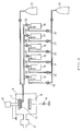
- An exhaust system 11 is fixed to one side of reaction chamber 6 to keep the chamber at low pressure.
- Carburetors 13-18 containing materials of this example are connected to an argon bomb 31 containing carrier gas through valves 19-24. By opening and closing valves 25-30, the introduction of the gas along with carrier gas into reaction chamber 6 can be controlled.
- An oxygen bomb 32 is connected to a pipe which has its open end between electrode 8 and substrate 10.
- the thin film capacitor of this example was manufactured as follows.
- a 100nm thick Pt layer was formed on the Si substrate by a sputtering treatment with a rf magnetron sputtering apparatus at 50W plasma power, 600°C substrate temperature and 1.4 Pa gas pressure for 14 minutes.
- the Si substrate formed with the Pt layer was attached to the bottom of electrode 7 shown in Fig. 2, and heated to 600°C.
- another thin film capacitor (1-b) was manufactured by forming a Ba 1-X Sr X TiO3 layer directly on a platinum layer, which was formed on a Si substrate by a plasma-enhanced CVD method, and then a counter-electrode (platinum) by a sputtering method.
- the film compositions of thin film capacitors (1-a) and (1-b) were analyzed with an electron probe X-ray microanalyzer. According to the analyses, the dielectric layers of these capacitors were Ba 0.7 Sr 0.3 TiO3.
- the dielectric constant and dielectric loss (1kHz, 1V) of thin film capacitor (1-a) at room temperature measured by a LCR (inductance-capacitance-resistance) meter were 4,200 and 1.4%.
- Thin film capacitor (1-b) had a 2,800 dielectric constant and 1.8% dielectric loss. The insulation resistance of these capacitors was higher than 109 ⁇ ⁇ cm.
- Thin film capacitor (1-a) had 1.8MV/cm direct current breakdown voltage while the capacitor (1-b) had 1.4MV/cm.
- a NiO layer, a Ba 0.7 Sr 0.3 TiO3 layer, and a Ba 0.7 Sr 0.3 TiO3/NiO film were individually formed on Si substrates.
- the crystal structures and the crystal orientations of the layers and the film were analyzed by reflection high-energy electron diffraction (RHEED) and X-ray diffraction. According to the analyses, the NiO layer was oriented to (100) face.
- the Ba 0.7 Sr 0.3 TiO3 layer formed on the oriented NiO layer (Ba 0.7 Sr 0.3 TiO3 layer of the Ba 0.7 Sr 0.3 TiO3/NiO film) showed stronger (100) orientation and higher crystallinity than the Ba 0.7 Sr 0.3 TiO3 layer formed directly on the substrate.
- the cross section and the surface of the Ba 0.7 Sr 0.3 TiO3/NiO film were observed with a high resolution scanning electron microscope. According to the observation, the Ba 0.7 Sr 0.3 TiO3 layer of the film was significantly dense, and its particle size was about 0.20 ⁇ m.
- ⁇ -diketone metal complex was used as a source material for a NaCl oxide layer.
- Ba(DPM), Sr(DPM)2, Ti(C3H7O)4 or Ti(DPM)2 ⁇ (C3H7O)2, Pb(DPM)2 or Pb(C2H5)4, Mg(DPM)2 or Mg(acac)2, and Nb(C2H5O)5 or Nb(DPM)2 ⁇ Cl3 were used.
- a metal electrode Besides Pt, nickel, palladium, silver/palladium alloy, copper or the like can be used for a metal electrode.
- the characteristics of a thin film capacitor are the same with any of the methods including a sputtering method, vacuum deposition method, CVD method and plasma-enhanced CVD method.
- Fig. 3 shows a thin film capacitor of this example having a platinum layer 36 (metal electrode), a Ni 0.5 Fe 2.5 O4 layer 37 (spinel oxide thin layer oriented to (100) face), a Ba 0.8 Sr 0.2 TiO3 layer 38 (perovskite dielectric thin layer oriented to (100) face) and a platinum layer 39 (metal electrode) sequentially laminated on the surface of a Si substrate 35.
- a platinum layer 36 metal electrode
- Ni 0.5 Fe 2.5 O4 layer 37 spinel oxide thin layer oriented to (100) face
- Ba 0.8 Sr 0.2 TiO3 layer 38 perovskite dielectric thin layer oriented to (100) face
- platinum layer 39 metal electrode
- the thin film capacitor of this example was manufactured as follows.
- a 100nm thick Pt layer was formed on Si substrate 35 by a sputtering treatment with a rf magnetron sputtering apparatus at 50W plasma power, 600°C substrate temperature and 1.4 Pa gas pressure for 14 minutes. Then, Si substrate 35 formed with the Pt layer (Pt layer/Si substrate) was attached to the bottom surface of electrode 7 shown in Fig. 2, and heated to 600°C.
- a Ba 1-X Sr X TiO3 layer was formed directly by a plasma-enhanced CVD method, and a counter-electrode (platinum) was formed on the Ba 1-X Sr X TiO3 layer by a sputtering method. As a result, a thin film capacitor (2-b) was manufactured.
- the film compositions of thin film capacitors (2-a) and (2-b) were analyzed with an electron probe X-ray microanalyzer. According to the analyses, the foundation layer of the capacitor (2-a) was Ni 0.5 Fe 2.5 O4, and the dielectric layers of capacitors (2-a) and (2-b) were Ba 0.8 Sr 0.2 TiO3.
- the dielectric constant and the dielectric loss (1kHz, 1V) of the capacitor (2-a) at room temperature measured by a LCR meter were 3,100 and 2.0% while those of the capacitor (2-b) were 2,800 and 2.9%.
- the insulation resistance of the capacitors (2-a) and (2-b) was above 109 ⁇ ⁇ cm.
- the direct current breakdown voltage of the capacitor (2-a) was 1.7 MV/cm while that of the capacitor (2-b) was 1.2 MV/cm.
- a platinum layer, a Ni 0.5 Fe 2.5 O4 layer, a Ba 0.8 Sr 0.2 TiO3 layer, and a Ba 0.8 Sr 0.2 TiO3/Ni 0.5 Fe 2.5 O4 film were individually formed on Si substrates. Then, the crystal structures and the crystal orientations of the layers and the film were observed by RHEED and X-ray diffraction. According to the observation, the Ni 0.5 Fe 2.5 O4 layer was oriented to (100) face.
- the Ba 0.8 Sr 0.2 TiO3 layer formed on the oriented Ni 0.5 Fe 2.5 O4 layer (Ba 0.8 Sr 0.2 TiO3 layer of the Ba 0.8 Sr 0.2 TiO3/Ni 0.5 Fe 2.5 O4 film) had better (100) orientation and crystallinity than the Ba 0.8 Sr 0.2 TiO3 layer directly formed on the substrate.
- the cross section and the surface of the Ba 0.8 Sr 0.2 TiO3/Ni 0.5 Fe 2.5 O4 film were observed by a high resolution scanning electron microscope. According to the observation, the Ba 0.8 Sr 0.2 TiO3 layer of the film was significantly dense, and the particle size was about 0.22 ⁇ m.
- ⁇ -diketone metal complex was used as a source material for a spinel oxide layer.
- a perovskite dielectric layer was formed by using Ba(DPM)2, Sr(DPM)2, Ti(C3H7O)4 or Ti(DPM)2 ⁇ (C3H7O)2, Pb(DPM)2 or Pb(C2H5)4, Mg(DPM)2 or Mg(acac)2 and Nb(C2H5O)5 or Nb(DPM)2Cl3.
- metals such as nickel, palladium, silver/palladium alloy, copper or the like can be used as a metal electrode.
- the properties of thin film capacitors are the same with any of these methods including a sputtering method, a vacuum deposition method, a CVD method, and a plasma-enhanced CVD method.
- Fig. 4 shows a thin film capacitor of this example having a NiO layer 42 (NaCl oxide thin layer oriented to (100) face), a platinum layer 43 (metal electrode), a Ba 0.5 Sr 0.5 TiO3 layer 44 (perovskite dielectric thin layer oriented to (100) face) and a platinum layer 45 (metal electrode) sequentially laminated on a Si substrate 41.
- NiO layer 42 NiCl oxide thin layer oriented to (100) face
- platinum layer 43 metal electrode
- Ba 0.5 Sr 0.5 TiO3 layer 44 perovskite dielectric thin layer oriented to (100) face
- platinum layer 45 metal electrode
- the thin film capacitor of this example were manufactured as follows.
- NiO layer As a result, a 60nm thick NiO layer was formed on substrate 10, which was heated to 600°C and rotated 120 times per minute. Then, valves 23 and 29 were closed. After cooling the NiO layer/Si substrate to room temperature, it was removed from the chamber. Due to a sputtering treatment with a rf magnetron sputtering apparatus at 40W plasma, 1.0 Pa gas pressure and 600°C substrate temperature for 20 minutes, a 80nm thick platinum thin layer was formed on the surface of the NiO layer (Pt layer/NiO layer/Si substrate).
- the Pt layer/NiO layer/Si substrate was taken out of the sputtering apparatus after being cooled to room temperature. Then, it was fixed to the bottom surface of electrode 7 of the plasma-enhanced CVD device shown in Fig. 2.
- the pressure inside the reaction chamber was reduced by exhaust system 11, and the Pt layer/NiO layer/Si substrate was heated to 600°C in the chamber.
- vaporized barium dipivaloylmethane, strontium dipivaloylmethane and titanium tetraisopropoxide were introduced to the reaction chamber by argon carrier gas, which entered carburetors 13, 14 and 15 at 25 SCCM, 3 030 SCCM and 5 SCCM flow rates respectively.
- Oxygen was also introduced to reaction chamber 6 at a 10 SCCM flow rate, thus generating reaction with 1.4W/cm2 electric power plasma at 7 Pa for 15 minutes in the chamber.
- a 2.2 ⁇ m thick Ba 1-X Sr X TiO3 layer was formed on the surface of the Pt layer.
- the Si substrate formed with the Ba 1-X Sr X TiO3/Pt/NiO film was removed from the vacuum reaction chamber, and a 100nm thick counter-electrode (platinum layer) was formed on the surface of the Si substrate by a sputtering treatment at 50W plasma power, 1.4 Pa gas pressure and 600°C substrate temperature for 15 minutes.
- a thin film capacitor (3-a) was manufactured.
- a Pt layer was directly formed on a Si substrate by a sputtering method without forming a NiO layer between the Pt layer and the substrate. Then, a Ba 1-X Sr X TiO3 layer was formed on the Pt layer by a plasma-enhanced CVD method, and a counter-electrode (platinum) was formed on the Ba 1-X Sr X TiO3 layer by a sputtering method. Thus, a thin film capacitor (3-b) was manufactured.
- the compositions of dielectric layers of the capacitors (3-a) and (3-b) were Ba 0.5 Sr 0.5 TiO3.
- the dielectric constant and the dielectric loss (1kHz, 1V) of the capacitor (3-a) at room temperature were 4,000 and 1.7% respectively by a LCR meter, and those of the capacitor (3-b) were 2,100 and 1.8%.
- the insulation resistance of the capacitors (3-a) and (3-b) was above 109 ⁇ ⁇ cm.
- the direct current breakdown voltage of the capacitor (3-a) was 1.8MV/cm while that of the capacitor (3-b) was 1.5MV/cm.
- a NiO layer, a Pt layer, a Pt/NiO film, a Ba 0.5 Sr 0.5 TiO3 layer, and a Ba 0.5 Sr 0.5 TiO3/Pt/NiO film were individually formed on Si substrates.
- the crystal compositions and the crystal orientations of the layers and the film were observed by RHEED and X-ray diffraction. According to the observation, it was found that the NiO layer was oriented to (100) face.
- the Pt layer on the other hand, showed no orientation.
- the Pt layer of the Pt/NiO film was oriented to (100) face.
- the Ba 0.5 Sr 0.5 TiO3 layer formed on the oriented Pt layer (Ba 0.5 Sr 0.5 TiO3 layer of the Ba 0.5 Sr 0.5 TiO3/Pt/NiO film) showed a stronger (100) orientation property and crystallinity than the Ba 0.5 Sr 0.5 TiO3 layer directly formed on the substrate.
- the cross section and the surface of the Ba 0.5 Sr 0.5 TiO3/Pt/NiO film were observed with a high resolution scanning electron microscope. According to the observation, the Ba 0.5 Sr 0.5 TiO3 layer of the film was highly dense, and the particle size was about 0.2 ⁇ m.
- ⁇ -diketone metal complex was used as a source material for a NaCl oxide layer.
- a perovskite dielectric thin layer was formed by using Ba(DPM)2, Sr(DPM)2, Ti(C3H7O)4 or Ti(DPM)2 ⁇ (C3H7O)2, Pb(DPM)2 or Pb(C2H5)4, Mg(DPM)2 or Mg(acac)2 and Nb(C2H5O)5 or Nb(DPM)2Cl3.
- metals such as nickel, palladium, silver/palladium alloy, copper or the like can be used for a metal electrode.
- the properties of thin film capacitors remain the same with any of methods including a sputtering method, a vacuum deposition method, a CVD method, and a plasma-enhanced CVD method.
- Fig. 5 shows a thin film capacitor of this example having a Ni 0.5 Fe 2.5 O4 layer 52 (spinel oxide thin layer oriented to (100) face), a platinum layer 53 (metal electrode), a Ba 0.6 Sr 0.4 TiO3 layer 54 (perovskite dielectric thin layer oriented to (100) face) and a platinum layer 55 (metal electrode) sequentially laminated on a Si substrate 51.
- Ni 0.5 Fe 2.5 O4 layer 52 spinel oxide thin layer oriented to (100) face
- platinum layer 53 metal electrode
- Ba 0.6 Sr 0.4 TiO3 layer 54 perovskite dielectric thin layer oriented to (100) face
- platinum layer 55 metal electrode
- the thin film capacitor was manufactured as follows.
- reaction chamber 6 After opening valves 23, 24, 29 and 30, vaporized nickel acetylacetonate and iron acetylacetonate along with argon carrier gas, which entered carburetors 17 and 18 at 20SCCM and 30 SCCM flow rates respectively, and oxygen at a 15 SCCM flow rate entered into reaction chamber 6.
- the reaction was carried out for four minutes in the chamber, depressurized to 5 Pa, with 1.4W/cm2 electric power plasma and at 550°C substrate temperature.
- the substrate was also rotated 120 times per minute. As a result, a 90nm thick Ni X Fe 3-X O4 layer was formed on the substrate. Valves 23, 24, 29 and 30 were then closed.
- the Si substrate formed with the Ni X Fe 3-X O4 layer After cooling the Si substrate formed with the Ni X Fe 3-X O4 layer to room temperature, it was removed from the chamber. Due to a sputtering treatment with a rf magnetron sputtering apparatus at 40W plasma power, 1.0 Pa gas pressure and 600°C substrate temperature for 25 minutes, a 100nm thick Pt layer was formed on the surface of the Ni X Fe 3-X O4 layer.
- the Si substrate formed with Pt/Ni X Fe 3-X O4 film was taken out of the sputtering apparatus after being cooled to room temperature. Then, the substrate was fixed to the bottom surface of electrode 7 shown in Fig. 2. The pressure inside the reaction chamber was reduced by exhaust system 11, and the Si substrate was heated to 600°C in the chamber. After opening valves 19, 20, 21, 25, 26 and 27, vaporized barium dipivaloylmethane, strontium dipivaloylmethane and titanium tetraisopropoxide were introduced to the reaction chamber by argon carrier gas, which entered carburetors 13, 14 and 15 at 25, 30 and 5 SCCM flow rates respectively.
- Oxygen was also introduced to reaction chamber 6 at a 10 SCCM flow rate, thus generating reaction at 1.4W/cm2 electric power plasma and 7 Pa for 15 minutes in the chamber.
- a 1.9 ⁇ m thick Ba 1-X Sr X TiO3 layer was formed on the surface of the Pt/Ni X Fe 3-X O4 film.
- the Si substrate formed with the Ba 1-X Sr X TiO3/Pt/Ni X Fe 3-X O4 film was taken out of the vacuum reaction chamber, and a 100nm thick counter-electrode (platinum layer) was formed on the surface of the Si substrate by a sputtering treatment at 50W plasma power, 1.4 Pa gas pressure and 600°C substrate temperature for 15 minutes.
- a thin film capacitor (4-a) was manufactured.
- a Ba 1-X Sr X TiO3 layer was directly formed on a Si substrate by a plasma-enhanced CVD method without forming a Pt/Ni X Fe 3-X O4 layer in between. Then, a counter-electrode (platinum) was formed on the surface of the Ba 1-X Sr X TiO3 layer by a sputtering method at 50W plasma power, 1.4Pa gas pressure and 600°C substrate temperature for 15 minutes. Thus, a thin film capacitor (4-b) was manufactured.
- compositions of dielectric layers of the capacitors (3-a) and (3-b) were Ba 0.6 Sr 0.4 TiO3.
- the composition of the spinel oxide thin layer of the capacitor (4-a) was Ni 0.5 Fe 2.5 O4.
- the dielectric constant and the dielectric loss (1kHz, 1V) of the capacitor (4-a) at room temperature measured by a LCR meter were 4,100 and 1.8% and those of the capacitor (4-b) were 2,100 and 1.8%.
- the insulation resistance of the capacitors (4-a) and (4-b) was above 109 ⁇ ⁇ cm.
- the direct current breakdown voltage of the capacitor (4-a) was 1.7MV/cm while that of the capacitor (4-b) was 1.2MV/cm.
- a Ni 0.5 Fe 2.5 O4 layer, a Pt layer, a Ba 0.6 Sr 0.4 TiO3 layer and a Ba 0.6 Sr 0.4 TiO3/Pt/Ni 0.5 Fe 2.5 O4 film were individually formed on Si substrates.
- the crystal compositions and the crystal orientations of the layers and the film were observed by RHEED and X-ray diffraction. According to the observation, it was found that the Ni 0.5 Fe 2.5 O4 layer was oriented to (100) face.
- the Pt layer showed no orientation.
- the Ba 0.6 Sr 0.4 TiO3 layer formed on the Pt/Ni 0.5 Fe 2.5 O4 film showed higher (100) orientation and crystallinity than the Ba 0.6 Sr 0.4 TiO3 layer directly formed on the substrate surface.
- the cross section and the surface of the Ba 0.6 Sr 0.4 TiO3/Pt/Ni 0.5 Fe 2.5 O4 film were observed by a high resolution scanning electron microscope. According to the observation, the Ba 0.6 Sr 0.4 TiO3 layer of the film was highly dense, and the particle size was about 0.22 ⁇ m.
- ⁇ -diketone metal complex was used as a source material for a spinel oxide layer.
- a perovskite dielectric thin layer was formed by using Ba(DPM)2, Sr(DPM)2, Ti(C3H7O)4 or Ti(DPM)2 ⁇ (C3H7O)2, Pb(DPM)2 or Pb(C2H5)4, Mg(DPM)2 or Mg(acac)2 and Nb(C2H5O)5 or Nb(DPM)2Cl3.
- metals such as nickel, palladium, silver/palladium alloy, copper or the like can be used for a metal electrode.
- the properties of thin film capacitors are the same with any of the methods including a sputtering method, a vacuum deposition method, a CVD method, and a plasma-enhanced CVD method.
- a NiO layer 62 NaCl oxide thin layer oriented to (100) face
- a Ba 0.7 Sr 0.3 TiO3 layer 63 perovskite dielectric thin layer oriented to (100) face
- a platinum layer 64 metal electrode
- the thin film capacitor of this example was manufactured as follows.
- a platinum substrate Pt layer/Si substrate
- a Ba 1-X Sr X TiO3 layer was formed directly on a Si substrate by a plasma-enhanced CVD method, and a counter-electrode (platinum) was formed on the Ba 1-X Sr X TiO3 layer by a sputtering method. As a result, a thin film capacitor (6-b) was manufactured.
- the film compositions of thin film capacitors (6-a) and (6-b) were analyzed with an electron probe X-ray microanalyzer. According to the analyses, the dielectric layers of capacitors (6-a) and (6-b) were Ba 0.7 Sr 0.3 TiO3.
- the dielectric constant and the dielectric loss (1kHz, 1V) of the capacitor (6-a) at room temperature measured by a LCR meter were 4,300 and 1.5% respectively while those of the capacitor (6-b) were 2,700 and 1.9%.
- the insulation resistance of the capacitors (6-a) and (6-b) was above 109 ⁇ ⁇ cm.
- the direct current breakdown voltage of the capacitor (6-a) was 1.9 MV/cm while that of the capacitor (6-b) was 1.6 MV/cm.
- a NiO layer, a Ba 0.7 Sr 0.3 TiO3 layer and a Ba 0.7 Sr 0.3 TiO3/NiO film were individually formed on platinum substrates. Then, the crystal structures and the crystal orientations of the layers and the film were observed by RHEED and X-ray diffraction. According to the observation, the NiO layer was oriented to (100) face.
- the Ba 0.7 Sr 0.3 TiO3 layer formed on the oriented NiO layer (Ba 0.7 Sr 0.3 TiO3 layer of the Ba 0.7 Sr 0.3 TiO3/NiO film) had better (100) orientation and crystallinity than the Ba 0.7 Sr 0.3 TiO3 layer directly formed on the substrate.
- the cross section and the surface of the Ba 0.7 Sr 0.3 TiO3/NiO film were observed with a high resolution scanning electron microscope. According to the observation, the Ba 0.7 Sr 0.3 TiO3 layer of the film was significantly dense, and the particle size was about 0.20 ⁇ m.
- ⁇ -diketone metal complex was used as a source material for a NaCl oxide layer and a spinel oxide layer.
- a perovskite dielectric layer was formed by using Ba(DPM)2, Sr(DPM)2, Ti(C3H7O)4 or Ti(DPM)2 ⁇ (C3H7O)2, Pb(DPM)2 or Pb(C2H5)4, Mg(DPM)2 or Mg(acac)2 and Nb(C2H5O)5 or Nb(DPM)2Cl3.
- metal electrode In addition to Pt, other metals such as nickel, palladium, silver/palladium alloy, copper or the like can be used as the metal electrode.
- the properties of thin film capacitors are the same with any of these methods including a sputtering method, a vacuum deposition method, a CVD method, and a plasma-enhanced CVD method.
- Fig. 7 shows a perspective view of a thin film capacitor.
- This thin film capacitor was manufactured by the method of this example as described above. Then, the substrate was cut to 3.3mm ⁇ 1.6mm; metal cables 75 were soldered to the surface of each metal electrode; and epoxy resin 76 was molded over the entire surface. The capacity of this thin film capacitor was 100pF.
- 71 indicates a metal electrode (platinum substrate); 72 shows a NaCl oxide thin layer or a spinel oxide thin layer; 73 is a perovskite dielectric thin layer; and 74 indicates a metal electrode (platinum layer).
Landscapes
- Engineering & Computer Science (AREA)
- Power Engineering (AREA)
- Manufacturing & Machinery (AREA)
- Microelectronics & Electronic Packaging (AREA)
- Fixed Capacitors And Capacitor Manufacturing Machines (AREA)
- Semiconductor Memories (AREA)
Applications Claiming Priority (3)
| Application Number | Priority Date | Filing Date | Title |
|---|---|---|---|
| JP6631793 | 1993-03-25 | ||
| JP66317/93 | 1993-03-25 | ||
| JP6631793 | 1993-03-25 |
Publications (3)
| Publication Number | Publication Date |
|---|---|
| EP0617439A2 true EP0617439A2 (de) | 1994-09-28 |
| EP0617439A3 EP0617439A3 (en) | 1997-10-15 |
| EP0617439B1 EP0617439B1 (de) | 2003-01-08 |
Family
ID=13312340
Family Applications (1)
| Application Number | Title | Priority Date | Filing Date |
|---|---|---|---|
| EP94104693A Expired - Lifetime EP0617439B1 (de) | 1993-03-25 | 1994-03-24 | Dünnschichtkondensator und Herstellungsverfahren |
Country Status (3)
| Country | Link |
|---|---|
| US (1) | US5406445A (de) |
| EP (1) | EP0617439B1 (de) |
| DE (1) | DE69431971T2 (de) |
Cited By (5)
| Publication number | Priority date | Publication date | Assignee | Title |
|---|---|---|---|---|
| US6025257A (en) * | 1996-03-13 | 2000-02-15 | Lg Semicon Co., Ltd. | Method for preparing dielectric thin film and semiconductor device using same |
| US6660535B2 (en) | 1999-08-25 | 2003-12-09 | Micronbtechnology, Inc. | Method of forming haze- free BST films |
| US7691780B2 (en) | 2004-12-22 | 2010-04-06 | Brookhaven Science Associates, Llc | Platinum- and platinum alloy-coated palladium and palladium alloy particles and uses thereof |
| US7855021B2 (en) | 2004-12-22 | 2010-12-21 | Brookhaven Science Associates, Llc | Electrocatalysts having platium monolayers on palladium, palladium alloy, and gold alloy core-shell nanoparticles, and uses thereof |
| US9005331B2 (en) | 2004-12-22 | 2015-04-14 | Brookhaven Science Associates, Llc | Platinum-coated non-noble metal-noble metal core-shell electrocatalysts |
Families Citing this family (10)
| Publication number | Priority date | Publication date | Assignee | Title |
|---|---|---|---|---|
| US5760432A (en) * | 1994-05-20 | 1998-06-02 | Kabushiki Kaisha Toshiba | Thin film strained layer ferroelectric capacitors |
| US5578846A (en) * | 1995-03-17 | 1996-11-26 | Evans, Jr.; Joseph T. | Static ferroelectric memory transistor having improved data retention |
| JP3094868B2 (ja) * | 1995-09-07 | 2000-10-03 | 三菱マテリアル株式会社 | 高純度誘電体薄膜の作製方法 |
| US5798903A (en) * | 1995-12-26 | 1998-08-25 | Bell Communications Research, Inc. | Electrode structure for ferroelectric capacitor integrated on silicon |
| US5777356A (en) * | 1996-01-03 | 1998-07-07 | Bell Communications Research, Inc. | Platinum-free ferroelectric memory cell with intermetallic barrier layer and method of making same |
| JP3612839B2 (ja) * | 1996-02-13 | 2005-01-19 | 三菱電機株式会社 | 高誘電率薄膜構造、高誘電率薄膜形成方法および高誘電率薄膜形成装置 |
| US5882410A (en) * | 1996-10-01 | 1999-03-16 | Mitsubishi Denki Kabushiki Kaisha | High dielectric constant thin film structure, method for forming high dielectric constant thin film, and apparatus for forming high dielectric constant thin film |
| US6194754B1 (en) * | 1999-03-05 | 2001-02-27 | Telcordia Technologies, Inc. | Amorphous barrier layer in a ferroelectric memory cell |
| TWI255057B (en) * | 2004-02-27 | 2006-05-11 | Canon Kk | Dielectric element, piezoelectric element, ink jet head and ink jet recording apparatus and manufacturing method of same |
| WO2019054474A1 (ja) | 2017-09-15 | 2019-03-21 | 国立研究開発法人科学技術振興機構 | チタン酸アルカリ土類金属結晶積層体 |
Citations (1)
| Publication number | Priority date | Publication date | Assignee | Title |
|---|---|---|---|---|
| EP0514149A1 (de) * | 1991-05-16 | 1992-11-19 | Nec Corporation | Dünnschichtkondensator |
Family Cites Families (7)
| Publication number | Priority date | Publication date | Assignee | Title |
|---|---|---|---|---|
| JPS63237514A (ja) * | 1987-03-26 | 1988-10-04 | 松下電器産業株式会社 | 薄膜コンデンサ |
| US5006363A (en) * | 1988-12-08 | 1991-04-09 | Matsushita Electric Industries Co., Ltd. | Plasma assited MO-CVD of perooskite dalectric films |
| JPH04184911A (ja) * | 1990-11-20 | 1992-07-01 | Toshiba Corp | 薄膜コンデンサ |
| US5142437A (en) * | 1991-06-13 | 1992-08-25 | Ramtron Corporation | Conducting electrode layers for ferroelectric capacitors in integrated circuits and method |
| JPH05235416A (ja) * | 1992-02-21 | 1993-09-10 | Murata Mfg Co Ltd | 強誘電体薄膜素子 |
| US5212620A (en) * | 1992-03-03 | 1993-05-18 | Radiant Technologies | Method for isolating SiO2 layers from PZT, PLZT, and platinum layers |
| US5323023A (en) * | 1992-12-02 | 1994-06-21 | Xerox Corporation | Epitaxial magnesium oxide as a buffer layer on (111) tetrahedral semiconductors |
-
1994
- 1994-03-24 US US08/216,966 patent/US5406445A/en not_active Expired - Lifetime
- 1994-03-24 DE DE69431971T patent/DE69431971T2/de not_active Expired - Lifetime
- 1994-03-24 EP EP94104693A patent/EP0617439B1/de not_active Expired - Lifetime
Patent Citations (1)
| Publication number | Priority date | Publication date | Assignee | Title |
|---|---|---|---|---|
| EP0514149A1 (de) * | 1991-05-16 | 1992-11-19 | Nec Corporation | Dünnschichtkondensator |
Cited By (7)
| Publication number | Priority date | Publication date | Assignee | Title |
|---|---|---|---|---|
| US6025257A (en) * | 1996-03-13 | 2000-02-15 | Lg Semicon Co., Ltd. | Method for preparing dielectric thin film and semiconductor device using same |
| US6660535B2 (en) | 1999-08-25 | 2003-12-09 | Micronbtechnology, Inc. | Method of forming haze- free BST films |
| US6852593B2 (en) | 1999-08-25 | 2005-02-08 | Micron Technology, Inc. | Haze-free BST films |
| US6939723B2 (en) | 1999-08-25 | 2005-09-06 | Micron Technology, Inc. | Method of forming haze-free BST films |
| US7691780B2 (en) | 2004-12-22 | 2010-04-06 | Brookhaven Science Associates, Llc | Platinum- and platinum alloy-coated palladium and palladium alloy particles and uses thereof |
| US7855021B2 (en) | 2004-12-22 | 2010-12-21 | Brookhaven Science Associates, Llc | Electrocatalysts having platium monolayers on palladium, palladium alloy, and gold alloy core-shell nanoparticles, and uses thereof |
| US9005331B2 (en) | 2004-12-22 | 2015-04-14 | Brookhaven Science Associates, Llc | Platinum-coated non-noble metal-noble metal core-shell electrocatalysts |
Also Published As
| Publication number | Publication date |
|---|---|
| DE69431971D1 (de) | 2003-02-13 |
| US5406445A (en) | 1995-04-11 |
| EP0617439B1 (de) | 2003-01-08 |
| DE69431971T2 (de) | 2003-11-27 |
| EP0617439A3 (en) | 1997-10-15 |
Similar Documents
| Publication | Publication Date | Title |
|---|---|---|
| EP0617439B1 (de) | Dünnschichtkondensator und Herstellungsverfahren | |
| US5663089A (en) | Method for producing a laminated thin film capacitor | |
| US20040175585A1 (en) | Barium strontium titanate containing multilayer structures on metal foils | |
| KR100292288B1 (ko) | 산소를사용하여우선배향성이조절된백금박막을형성하는방법및장치 | |
| KR20040036744A (ko) | 박막 용량 소자용 조성물, 고유전율 절연막, 박막 용량소자 및 박막 적층 콘덴서 | |
| KR20010031913A (ko) | 유전체 소자와 그 제조 방법 | |
| US6162293A (en) | Method for manufacturing ferroelectric thin film, substrate covered with ferroelectric thin film, and capacitor | |
| Sakabe et al. | Multilayer ceramic capacitors with thin (Ba, Sr) TiO 3 layers by MOCVD | |
| US7095067B2 (en) | Oxidation-resistant conducting perovskites | |
| JP3209633B2 (ja) | 薄膜コンデンサ及びその製造方法 | |
| CN1755848A (zh) | 电介质薄膜、薄膜电容元件及其制造方法 | |
| KR20040034671A (ko) | 박막 용량 소자용 조성물, 고유전율 절연막, 박막 용량소자 및 박막 적층 콘덴서 | |
| JP3328055B2 (ja) | 積層薄膜コンデンサの製造方法 | |
| JP3471655B2 (ja) | 高誘電体薄膜コンデンサの製造方法 | |
| EP1077478B1 (de) | Herstellungsmethode für einen ferroelektrischen dünnen Film, einen ferroelektrischen Kondensator und einen ferroelektrischen Speicher | |
| US20070040195A1 (en) | Monolithic integrated passive and active electronic devices with biocompatible coatings | |
| JPH07106198A (ja) | 積層薄膜コンデンサの製造方法 | |
| JP3389370B2 (ja) | セラミックコンデンサ | |
| JPH0959021A (ja) | ビスマス化合物の製造方法とビスマス化合物の誘電体物質 | |
| Lee et al. | Characterization of (Ba 1− x, Sr x) TiO 3 thin films deposited on Pt/Ti/SiO 2/Si substrates with different Ti buffer layer thicknesses | |
| JPH09326331A (ja) | (Ba,Sr)TiO3薄膜の製造方法およびそれを用いた薄膜コンデンサ | |
| KR100799847B1 (ko) | Pcb 내장형 박막 커패시터 및 그 제조방법 | |
| JPH10195656A (ja) | 酸化物薄膜の製造方法およびそれに用いる製造装置 | |
| JPH07283069A (ja) | 誘電体薄膜およびその製造方法 | |
| JPH0657411A (ja) | 誘電体薄膜の製造方法および装置 |
Legal Events
| Date | Code | Title | Description |
|---|---|---|---|
| PUAI | Public reference made under article 153(3) epc to a published international application that has entered the european phase |
Free format text: ORIGINAL CODE: 0009012 |
|
| AK | Designated contracting states |
Kind code of ref document: A2 Designated state(s): DE FR GB IT NL |
|
| PUAL | Search report despatched |
Free format text: ORIGINAL CODE: 0009013 |
|
| RHK1 | Main classification (correction) |
Ipc: H01G 4/06 |
|
| AK | Designated contracting states |
Kind code of ref document: A3 Designated state(s): DE FR GB IT NL |
|
| 17P | Request for examination filed |
Effective date: 19971017 |
|
| 18D | Application deemed to be withdrawn |
Effective date: 20001003 |
|
| D18D | Application deemed to be withdrawn (deleted) | ||
| GRAG | Despatch of communication of intention to grant |
Free format text: ORIGINAL CODE: EPIDOS AGRA |
|
| 17Q | First examination report despatched |
Effective date: 20011212 |
|
| GRAG | Despatch of communication of intention to grant |
Free format text: ORIGINAL CODE: EPIDOS AGRA |
|
| GRAG | Despatch of communication of intention to grant |
Free format text: ORIGINAL CODE: EPIDOS AGRA |
|
| GRAH | Despatch of communication of intention to grant a patent |
Free format text: ORIGINAL CODE: EPIDOS IGRA |
|
| GRAH | Despatch of communication of intention to grant a patent |
Free format text: ORIGINAL CODE: EPIDOS IGRA |
|
| GRAA | (expected) grant |
Free format text: ORIGINAL CODE: 0009210 |
|
| AK | Designated contracting states |
Kind code of ref document: B1 Designated state(s): DE FR GB IT NL |
|
| REG | Reference to a national code |
Ref country code: GB Ref legal event code: FG4D |
|
| REF | Corresponds to: |
Ref document number: 69431971 Country of ref document: DE Date of ref document: 20030213 Kind code of ref document: P |
|
| ET | Fr: translation filed | ||
| PLBE | No opposition filed within time limit |
Free format text: ORIGINAL CODE: 0009261 |
|
| STAA | Information on the status of an ep patent application or granted ep patent |
Free format text: STATUS: NO OPPOSITION FILED WITHIN TIME LIMIT |
|
| 26N | No opposition filed |
Effective date: 20031009 |
|
| PGFP | Annual fee paid to national office [announced via postgrant information from national office to epo] |
Ref country code: IT Payment date: 20120317 Year of fee payment: 19 |
|
| PGFP | Annual fee paid to national office [announced via postgrant information from national office to epo] |
Ref country code: DE Payment date: 20130320 Year of fee payment: 20 Ref country code: GB Payment date: 20130320 Year of fee payment: 20 Ref country code: FR Payment date: 20130325 Year of fee payment: 20 |
|
| PGFP | Annual fee paid to national office [announced via postgrant information from national office to epo] |
Ref country code: NL Payment date: 20130316 Year of fee payment: 20 |
|
| REG | Reference to a national code |
Ref country code: DE Ref legal event code: R071 Ref document number: 69431971 Country of ref document: DE |
|
| REG | Reference to a national code |
Ref country code: DE Ref legal event code: R071 Ref document number: 69431971 Country of ref document: DE |
|
| REG | Reference to a national code |
Ref country code: NL Ref legal event code: V4 Effective date: 20140324 |
|
| REG | Reference to a national code |
Ref country code: GB Ref legal event code: PE20 Expiry date: 20140323 |
|
| PG25 | Lapsed in a contracting state [announced via postgrant information from national office to epo] |
Ref country code: DE Free format text: LAPSE BECAUSE OF EXPIRATION OF PROTECTION Effective date: 20140325 Ref country code: GB Free format text: LAPSE BECAUSE OF EXPIRATION OF PROTECTION Effective date: 20140323 |