EP0617308A1 - Liquid crystal display with integrated electronics - Google Patents
Liquid crystal display with integrated electronics Download PDFInfo
- Publication number
- EP0617308A1 EP0617308A1 EP94301840A EP94301840A EP0617308A1 EP 0617308 A1 EP0617308 A1 EP 0617308A1 EP 94301840 A EP94301840 A EP 94301840A EP 94301840 A EP94301840 A EP 94301840A EP 0617308 A1 EP0617308 A1 EP 0617308A1
- Authority
- EP
- European Patent Office
- Prior art keywords
- plate member
- liquid crystal
- plate
- conductors
- crystal display
- Prior art date
- Legal status (The legal status is an assumption and is not a legal conclusion. Google has not performed a legal analysis and makes no representation as to the accuracy of the status listed.)
- Withdrawn
Links
Images
Classifications
-
- G—PHYSICS
- G02—OPTICS
- G02F—OPTICAL DEVICES OR ARRANGEMENTS FOR THE CONTROL OF LIGHT BY MODIFICATION OF THE OPTICAL PROPERTIES OF THE MEDIA OF THE ELEMENTS INVOLVED THEREIN; NON-LINEAR OPTICS; FREQUENCY-CHANGING OF LIGHT; OPTICAL LOGIC ELEMENTS; OPTICAL ANALOGUE/DIGITAL CONVERTERS
- G02F1/00—Devices or arrangements for the control of the intensity, colour, phase, polarisation or direction of light arriving from an independent light source, e.g. switching, gating or modulating; Non-linear optics
- G02F1/01—Devices or arrangements for the control of the intensity, colour, phase, polarisation or direction of light arriving from an independent light source, e.g. switching, gating or modulating; Non-linear optics for the control of the intensity, phase, polarisation or colour
- G02F1/13—Devices or arrangements for the control of the intensity, colour, phase, polarisation or direction of light arriving from an independent light source, e.g. switching, gating or modulating; Non-linear optics for the control of the intensity, phase, polarisation or colour based on liquid crystals, e.g. single liquid crystal display cells
- G02F1/133—Constructional arrangements; Operation of liquid crystal cells; Circuit arrangements
- G02F1/1333—Constructional arrangements; Manufacturing methods
- G02F1/1345—Conductors connecting electrodes to cell terminals
- G02F1/13452—Conductors connecting driver circuitry and terminals of panels
-
- H—ELECTRICITY
- H05—ELECTRIC TECHNIQUES NOT OTHERWISE PROVIDED FOR
- H05K—PRINTED CIRCUITS; CASINGS OR CONSTRUCTIONAL DETAILS OF ELECTRIC APPARATUS; MANUFACTURE OF ASSEMBLAGES OF ELECTRICAL COMPONENTS
- H05K1/00—Printed circuits
- H05K1/18—Printed circuits structurally associated with non-printed electric components
- H05K1/189—Printed circuits structurally associated with non-printed electric components characterised by the use of flexible or folded printed circuits
-
- H—ELECTRICITY
- H05—ELECTRIC TECHNIQUES NOT OTHERWISE PROVIDED FOR
- H05K—PRINTED CIRCUITS; CASINGS OR CONSTRUCTIONAL DETAILS OF ELECTRIC APPARATUS; MANUFACTURE OF ASSEMBLAGES OF ELECTRICAL COMPONENTS
- H05K2201/00—Indexing scheme relating to printed circuits covered by H05K1/00
- H05K2201/05—Flexible printed circuits [FPCs]
- H05K2201/056—Folded around rigid support or component
-
- H—ELECTRICITY
- H05—ELECTRIC TECHNIQUES NOT OTHERWISE PROVIDED FOR
- H05K—PRINTED CIRCUITS; CASINGS OR CONSTRUCTIONAL DETAILS OF ELECTRIC APPARATUS; MANUFACTURE OF ASSEMBLAGES OF ELECTRICAL COMPONENTS
- H05K2201/00—Indexing scheme relating to printed circuits covered by H05K1/00
- H05K2201/10—Details of components or other objects attached to or integrated in a printed circuit board
- H05K2201/10007—Types of components
- H05K2201/10128—Display
- H05K2201/10136—Liquid Crystal display [LCD]
-
- H—ELECTRICITY
- H05—ELECTRIC TECHNIQUES NOT OTHERWISE PROVIDED FOR
- H05K—PRINTED CIRCUITS; CASINGS OR CONSTRUCTIONAL DETAILS OF ELECTRIC APPARATUS; MANUFACTURE OF ASSEMBLAGES OF ELECTRICAL COMPONENTS
- H05K2201/00—Indexing scheme relating to printed circuits covered by H05K1/00
- H05K2201/10—Details of components or other objects attached to or integrated in a printed circuit board
- H05K2201/10613—Details of electrical connections of non-printed components, e.g. special leads
- H05K2201/10621—Components characterised by their electrical contacts
- H05K2201/10689—Leaded Integrated Circuit [IC] package, e.g. dual-in-line [DIL]
-
- H—ELECTRICITY
- H05—ELECTRIC TECHNIQUES NOT OTHERWISE PROVIDED FOR
- H05K—PRINTED CIRCUITS; CASINGS OR CONSTRUCTIONAL DETAILS OF ELECTRIC APPARATUS; MANUFACTURE OF ASSEMBLAGES OF ELECTRICAL COMPONENTS
- H05K2203/00—Indexing scheme relating to apparatus or processes for manufacturing printed circuits covered by H05K3/00
- H05K2203/13—Moulding and encapsulation; Deposition techniques; Protective layers
- H05K2203/1305—Moulding and encapsulation
- H05K2203/1311—Foil encapsulation, e.g. of mounted components
-
- H—ELECTRICITY
- H05—ELECTRIC TECHNIQUES NOT OTHERWISE PROVIDED FOR
- H05K—PRINTED CIRCUITS; CASINGS OR CONSTRUCTIONAL DETAILS OF ELECTRIC APPARATUS; MANUFACTURE OF ASSEMBLAGES OF ELECTRICAL COMPONENTS
- H05K3/00—Apparatus or processes for manufacturing printed circuits
- H05K3/36—Assembling printed circuits with other printed circuits
- H05K3/361—Assembling flexible printed circuits with other printed circuits
Definitions
- the present invention relates to liquid crystal displays, and more specifically to a liquid crystal display with integrated electronics.
- liquid crystal transparent, normally glass, screens for use in liquid crystal displays are manufactured as individual components, separate from the electronic circuits to which they are connected.
- the electronic circuits are generally part of a printed circuit board and may include circuitry for driving the liquid crystal glass screens, as well as a microprocessor.
- the electronic circuitry may be consolidated into as few separate components as possible, with the main processor and drive circuitry being located on a single chip.
- the liquid crystal glass screens are connected to the printed circuit board to form an LCD device. This known arrangement has the disadvantage that connection of the electronic circuits to the glass is difficult.
- a liquid crystal display device incorporating a first liquid crystal plate member the top surface of which includes a plurality of substantially parallel conductors, a second liquid crystal plate member, mounted on top of the first plate member, the bottom surface of which includes a plurality of substantially parallel conductors, wherein the conductors of the first plate member are substantially perpendicular to the conductors of the second plate member, characterized in that a flexible member is coupled to the conductors of the first and second plate members, said flexible member including a circuit having a driver circuit which drives the first and second plate members to form a liquid crystal display.
- a liquid crystal display device in accordance with the invention may additionally include at least one integrated circuit, which may include a microprocessor.
- the flexible member mounts on top of the second plate and the exposed portions of the first plate, and bends around the first plate to contact the bottom surface of the second plate at the first end.
- device 10 includes liquid crystal display (LCD) 12 and flexible electronic circuit assembly 14.
- LCD 12 includes upper and lower liquid crystal glass plates 16 and 18, which are hermetically sealed around their peripheries to enclose a cavity containing liquid crystal material.
- the liquid crystal material changes its light-polarizing behaviour when a voltage is applied.
- Flexible electronic circuit assembly 14 rests on top of both plates 16 and 18. It bends as necessary to contact top surface 20 of lower plate 18 and wraps around upper plate 16 to make contact with bottom surface 22. In the embodiment of Figure. 1, contact is made at opposite ends of lower plate 18, but only one end of upper plate 16. Another embodiment envisions contact being made at both ends of plate 16.
- Plate 16 includes transparent conductors 24 on bottom surface 22, and plate 18 includes transparent conductors 26 on top surface 20.
- Transparent conductors 24 and 26 are usually made of indium-tin oxide. When a voltage is applied between a given one of conductors 24 and a given one of conductors 26, the light-polarizing behaviour of the liquid crystal material causes incident light to be blocked, thereby creating the appearance of a dark spot where the conductors cross. It is common practice for high-resolution LCDs to interdigitate conductors 26 and to provide two points of contact, on opposite ends of plate 18, between integrated electronics assembly 14 and conductors 26. For such LCDs, the pitch of conductors 24 and 26 is typically six mils.
- integrated electronics assembly 14 primarily includes a flexible substrate 28 and integrated circuits (ICs) 30.
- Flexible substrate 28 may be any commercially-available high or low-temperature flexible substrate.
- the high-temperature flexible substrate is preferred if ICs 30 and other components are to be soldered to substrate 28.
- the low-temperature is preferred if ICs 30 and other components are to be glued to substrate 28 with a commercially-available conductive adhesive.
- the thermal coefficient of expansion of substrate 28 is approximately the same as that of plate 16 and 18.
- Substrate 28 includes electrical traces 32-36, wherein electrical traces 32 make contact with conductors 24, electrical traces 34 and 36 make contact with conductors 26 on opposite ends of glass plate 18, and electrical traces 38 make contact with other electronic components which may be part of the system containing device 10.
- traces 32-36 are soldered or glued to their respective conductors 24 and 26 with a commercially-available anisotropic conductive adhesive. This type of adhesive is conductive in the direction perpendicular to both the traces and conductors, and not conductive in any other direction.
- ICs 30 may be any commercially available integrated circuits. The ones shown are of the quad flat pack type. For computer applications, ICs 30 may contain as much computer circuitry as possible, including the main processor and additional components as necessary to form a complete data processing device. ICs 30 may be located on either side or on both sides of flexible substrate 28. If ICs 30 are to be located on the side opposite to that of traces 32-36, care must be taken to minimize the occurrence of short circuits at vias connecting traces on one side of flexible substrate 28 to the other.
- device 10 may be assembled by first aligning and bonding traces 32 to conductors 24. After these bonds are completed, flexible substrate 28 may be folded over upper glass plate 16. A compliant protective material may be included between upper glass plate 16 and flexible substrate 28 to protect top surface of upper glass 16. After substrate 28 is folded, traces 34 and 36 are aligned and bonded to conductors 26 to complete the assembly process.
Landscapes
- Physics & Mathematics (AREA)
- Nonlinear Science (AREA)
- Engineering & Computer Science (AREA)
- Microelectronics & Electronic Packaging (AREA)
- Mathematical Physics (AREA)
- Chemical & Material Sciences (AREA)
- Crystallography & Structural Chemistry (AREA)
- General Physics & Mathematics (AREA)
- Optics & Photonics (AREA)
- Liquid Crystal (AREA)
- Devices For Indicating Variable Information By Combining Individual Elements (AREA)
- Combinations Of Printed Boards (AREA)
Abstract
A liquid crystal display which has integrated electronics. The liquid crystal display includes a first liquid crystal plate (16) member having a bottom surface (22) and a plurality of substantially parallel conductors on the bottom surface, and a second liquid crystal plate member (18) mounted below the first plate member and having a top surface (20) and a plurality of substantially parallel conductors on the top surface. The conductors of the first plate member (16) are substantially perpendicular to the conductors of the second plate member (18). A flexible member (14) coupled to the liquid crystal display includes a circuit having a driver circuit which drives the first and second plate members to form the liquid crystal display. The circuit may also include at least one integrated circuit, as well as electrical traces which are coupled to conductors on the first and second plate members. The flexible member (14) mounts on top of the first plate member (16) and the exposed portions of the second plate member (18), and bends around the first plate member to contact the bottom surface (22) of the first plate member at the first end.
Description
- The present invention relates to liquid crystal displays, and more specifically to a liquid crystal display with integrated electronics.
- Typically, liquid crystal transparent, normally glass, screens for use in liquid crystal displays (LCDs) are manufactured as individual components, separate from the electronic circuits to which they are connected. The electronic circuits are generally part of a printed circuit board and may include circuitry for driving the liquid crystal glass screens, as well as a microprocessor. The electronic circuitry may be consolidated into as few separate components as possible, with the main processor and drive circuitry being located on a single chip. The liquid crystal glass screens are connected to the printed circuit board to form an LCD device. This known arrangement has the disadvantage that connection of the electronic circuits to the glass is difficult.
- A detailed description of the construction of LCDs can be found in the text "Electronic Display Devices", by Shoichi Matsumoto, published by John Wiley & Sons.
- It is an object of the present invention to provide a liquid crystal display in which the above mentioned difficulty is alleviated.
- According to the present invention there is provided a liquid crystal display device incorporating a first liquid crystal plate member the top surface of which includes a plurality of substantially parallel conductors, a second liquid crystal plate member, mounted on top of the first plate member, the bottom surface of which includes a plurality of substantially parallel conductors, wherein the conductors of the first plate member are substantially perpendicular to the conductors of the second plate member, characterized in that a flexible member is coupled to the conductors of the first and second plate members, said flexible member including a circuit having a driver circuit which drives the first and second plate members to form a liquid crystal display.
- A liquid crystal display device in accordance with the invention may additionally include at least one integrated circuit, which may include a microprocessor. The flexible member mounts on top of the second plate and the exposed portions of the first plate, and bends around the first plate to contact the bottom surface of the second plate at the first end.
- An embodiment of the present invention will now be described, by way of example, with reference to the accompanying drawings, in which:-
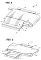
- Figure. 1 is a perspective view of a liquid crystal display with integrated electronics in accordance with the present invention;
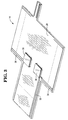
- Figure. 2 is a perspective view of the liquid crystal display of Figure 1; and
- Figure. 3 is a perspective view of the integrated electronics in accordance with the present invention.
- Referring now to Figure. 1,
device 10 includes liquid crystal display (LCD) 12 and flexibleelectronic circuit assembly 14.LCD 12 includes upper and lower liquidcrystal glass plates - Flexible
electronic circuit assembly 14 rests on top of bothplates top surface 20 oflower plate 18 and wraps aroundupper plate 16 to make contact withbottom surface 22. In the embodiment of Figure. 1, contact is made at opposite ends oflower plate 18, but only one end ofupper plate 16. Another embodiment envisions contact being made at both ends ofplate 16. - Referring now to Figure. 2, upper and
lower glass plates Plate 16 includestransparent conductors 24 onbottom surface 22, andplate 18 includestransparent conductors 26 ontop surface 20.Transparent conductors conductors 24 and a given one ofconductors 26, the light-polarizing behaviour of the liquid crystal material causes incident light to be blocked, thereby creating the appearance of a dark spot where the conductors cross. It is common practice for high-resolution LCDs tointerdigitate conductors 26 and to provide two points of contact, on opposite ends ofplate 18, between integratedelectronics assembly 14 andconductors 26. For such LCDs, the pitch ofconductors - Referring now to Figure. 3,
integrated electronics assembly 14 primarily includes aflexible substrate 28 and integrated circuits (ICs) 30.Flexible substrate 28 may be any commercially-available high or low-temperature flexible substrate. The high-temperature flexible substrate is preferred ifICs 30 and other components are to be soldered tosubstrate 28. The low-temperature is preferred ifICs 30 and other components are to be glued tosubstrate 28 with a commercially-available conductive adhesive. Preferably, the thermal coefficient of expansion ofsubstrate 28 is approximately the same as that ofplate -
Substrate 28 includes electrical traces 32-36, whereinelectrical traces 32 make contact withconductors 24,electrical traces conductors 26 on opposite ends ofglass plate 18, and electrical traces 38 make contact with other electronic components which may be part of thesystem containing device 10. Preferably, traces 32-36 are soldered or glued to theirrespective conductors - ICs 30 may be any commercially available integrated circuits. The ones shown are of the quad flat pack type. For computer applications,
ICs 30 may contain as much computer circuitry as possible, including the main processor and additional components as necessary to form a complete data processing device. ICs 30 may be located on either side or on both sides offlexible substrate 28. IfICs 30 are to be located on the side opposite to that of traces 32-36, care must be taken to minimize the occurrence of short circuits at vias connecting traces on one side offlexible substrate 28 to the other. - Referring now to Figures. 1-3,
device 10 may be assembled by first aligning and bondingtraces 32 toconductors 24. After these bonds are completed,flexible substrate 28 may be folded overupper glass plate 16. A compliant protective material may be included betweenupper glass plate 16 andflexible substrate 28 to protect top surface ofupper glass 16. Aftersubstrate 28 is folded, traces 34 and 36 are aligned and bonded toconductors 26 to complete the assembly process. - In view of the foregoing it will be clear to a person skilled in the art that modifications may be incorporated without departing from the scope of the present invention.
Claims (9)
- A liquid crystal display device (10) incorporating a first liquid crystal plate member (18) the top surface (20) of which includes a plurality of substantially parallel conductors (26), a second liquid crystal plate member (16), mounted on top of the first plate member (18), the bottom surface of which includes a plurality of substantially parallel conductors(24), wherein the conductors (26) of the first plate member are substantially perpendicular to the conductors (24) of the second plate member, characterized in that a flexible member (28) is coupled to the conductors (24,26) of the first and second plate members (16,18), said flexible member including a circuit (14) having a driver circuit (30) which drives the first and second plate members (16,18) to form a liquid crystal display.
- A device according to claim 1, characterized in that the conductors (26) of the first plate member (16), each have first and second ends which are exposed at first and second ends of the first plate member (16) and the conductors (24) of the second plate member (18) each have first ends which are exposed at a first end of the second plate member (18) for coupling the first and second plate members (16,18) to the flexible member (28).
- A device according to claim 1 or claim 2, characterized in that the circuit (14) further includes at least one electrical component (30) and a plurality of electrical traces (32-38) coupling the or each electrical component to the first and second plate members (16,18).
- A device according to claim 3, characterized in that the electrical component (30) comprises an integrated circuit.
- A device according to any of claims 2 to 4, characterized in that circuit (14) includes a first group of electrical traces (34), each of which is coupled to a conductor (26), on the first plate member at the first end thereof; a second group of electrical traces (36), each of which is coupled to a conductor (26) on the first plate member (16) at the second end thereof; and a third group of electrical traces (32), each of which is coupled to a conductor (24) on the second plate member (18) at the first end thereof.
- A device according to claim 5, wherein the flexible member (28) is located above the second plate member and the exposed ends of the first plate member and bends around the second plate member to contact the bottom surface of the second plate member at the first end thereof.
- A device according to any one of the preceding claims, characterized in that the device further includes a protective member (44) between the flexible member (28) and the second plate member (18).
- A device according to any of claims 3 to 7, characterized in that the circuit means (14) includes at least one electrical component (30) which is located on the same side of the flexible member as the traces (32-38).
- A device according to any of claims 3 to 7, characterized in that the circuit means comprises at least one electrical component (40) which is located on one side of the flexible member, the electrical traces (32-38) being located on both sides of the flexible member (28), wherein the flexible member has a via (42) through the flexible member for each trace which passes from one side of the flexible member to the other.
Applications Claiming Priority (2)
| Application Number | Priority Date | Filing Date | Title |
|---|---|---|---|
| US3499093A | 1993-03-22 | 1993-03-22 | |
| US34990 | 1993-03-22 |
Publications (1)
| Publication Number | Publication Date |
|---|---|
| EP0617308A1 true EP0617308A1 (en) | 1994-09-28 |
Family
ID=21879935
Family Applications (1)
| Application Number | Title | Priority Date | Filing Date |
|---|---|---|---|
| EP94301840A Withdrawn EP0617308A1 (en) | 1993-03-22 | 1994-03-15 | Liquid crystal display with integrated electronics |
Country Status (3)
| Country | Link |
|---|---|
| US (1) | US5563619A (en) |
| EP (1) | EP0617308A1 (en) |
| JP (1) | JPH0772494A (en) |
Cited By (3)
| Publication number | Priority date | Publication date | Assignee | Title |
|---|---|---|---|---|
| EP1533852A2 (en) * | 2003-11-21 | 2005-05-25 | Semiconductor Energy Laboratory Co., Ltd. | Organic electroluminescent display |
| EP1195818B1 (en) * | 2000-10-06 | 2018-01-10 | LG Display Co., Ltd. | Display device using cof |
| CN109688701A (en) * | 2018-06-26 | 2019-04-26 | 上海嘉捷通电路科技股份有限公司 | A kind of rigid-flexible combination pcb board |
Families Citing this family (11)
| Publication number | Priority date | Publication date | Assignee | Title |
|---|---|---|---|---|
| WO1996008746A1 (en) * | 1994-09-16 | 1996-03-21 | Seiko Epson Corporation | Liquid crystal display, its mounting structure, and electronic device |
| JP3442893B2 (en) * | 1995-01-27 | 2003-09-02 | 富士通株式会社 | Input device |
| EP0778959A1 (en) * | 1995-06-29 | 1997-06-18 | Koninklijke Philips Electronics N.V. | Display device |
| US6375615B1 (en) * | 1995-10-13 | 2002-04-23 | Transvascular, Inc. | Tissue penetrating catheters having integral imaging transducers and their methods of use |
| US6302875B1 (en) | 1996-10-11 | 2001-10-16 | Transvascular, Inc. | Catheters and related devices for forming passageways between blood vessels or other anatomical structures |
| JP4880833B2 (en) * | 2001-07-31 | 2012-02-22 | パナソニック株式会社 | Electronic component, component mounting apparatus, and component mounting method |
| JP3895697B2 (en) * | 2003-03-03 | 2007-03-22 | 日東電工株式会社 | Flexible printed circuit board |
| CN100358400C (en) * | 2004-03-22 | 2007-12-26 | 友达光电股份有限公司 | Flexible circuit board structure and electronic device for preventing stress concentration when it is bent |
| JP5292446B2 (en) * | 2011-09-02 | 2013-09-18 | パナソニック株式会社 | Component mounting apparatus and component mounting method |
| CN204884440U (en) * | 2015-08-27 | 2015-12-16 | 京东方科技集团股份有限公司 | Flexible display panel and flexible display device |
| USD914405S1 (en) | 2019-02-01 | 2021-03-30 | Target Brands, Inc. | Product display fixture |
Citations (5)
| Publication number | Priority date | Publication date | Assignee | Title |
|---|---|---|---|---|
| JPS5555276A (en) * | 1978-10-18 | 1980-04-23 | Seiko Epson Corp | Digital indication electronic watch structure |
| JPS5834434A (en) * | 1981-08-24 | 1983-02-28 | Seiko Instr & Electronics Ltd | Display device |
| JPS60208734A (en) * | 1984-04-02 | 1985-10-21 | Sharp Corp | Liquid crystal display device |
| DE3914527A1 (en) * | 1989-05-02 | 1990-11-08 | Licentia Gmbh | LIQUID CRYSTAL DISPLAY DEVICE |
| WO1992021051A1 (en) * | 1991-05-15 | 1992-11-26 | Idemitsu Kosan Co., Ltd. | Liquid crystal module |
Family Cites Families (18)
| Publication number | Priority date | Publication date | Assignee | Title |
|---|---|---|---|---|
| US3579206A (en) * | 1968-12-16 | 1971-05-18 | Rca Corp | Low inductance interconnection of cryoelectric memory system |
| CH520937A (en) * | 1970-05-27 | 1972-03-31 | Bbc Brown Boveri & Cie | Arrangement for displaying an electrical measurement voltage by means of a display medium extending over a large area between two electrodes |
| DE3035268C2 (en) * | 1979-09-19 | 1983-01-20 | Sharp K.K., Osaka | Multi-layer liquid crystal display panel |
| US4468659A (en) * | 1980-08-25 | 1984-08-28 | Sharp Kabushiki Kaisha | Electroluminescent display panel assembly |
| US4521775A (en) * | 1980-10-17 | 1985-06-04 | Texas Instruments Incorporated | Method of operating a stacked display |
| JPS57205711A (en) * | 1981-06-12 | 1982-12-16 | Ricoh Co Ltd | Liquid crystal display device |
| JPS5825615A (en) * | 1981-08-07 | 1983-02-15 | Sanyo Electric Co Ltd | Two-layered liquid-crystal panel |
| GB2124010B (en) * | 1982-07-13 | 1986-06-18 | Sharp Kk | Structure and method of connecting terminals of matrix display units |
| GB2134299B (en) * | 1982-12-23 | 1986-04-30 | Epson Corp | Liquid crystal display device |
| JPS60149079A (en) * | 1984-01-13 | 1985-08-06 | シャープ株式会社 | Connector for display body unit |
| DE3616046C2 (en) * | 1985-05-13 | 1996-04-25 | Ricoh Kk | Liquid crystal display device with a printed circuit board |
| JPS62280889A (en) * | 1986-05-30 | 1987-12-05 | シャープ株式会社 | Planar type display unit |
| JPS62289815A (en) * | 1986-06-09 | 1987-12-16 | Seiko Epson Corp | Liquid crystal display device |
| US4839634A (en) * | 1986-12-01 | 1989-06-13 | More Edward S | Electro-optic slate for input/output of hand-entered textual and graphic information |
| US4917466A (en) * | 1987-08-13 | 1990-04-17 | Shin-Etsu Polymer Co., Ltd. | Method for electrically connecting IC chips, a resinous bump-forming composition used therein and a liquid-crystal display unit electrically connected thereby |
| US5029984A (en) * | 1988-03-15 | 1991-07-09 | Mitsubishi Denki Kabushiki Kaisha | Liquid crystal display device |
| JPH07122714B2 (en) * | 1989-03-22 | 1995-12-25 | 松下電器産業株式会社 | Liquid crystal display |
| US5140107A (en) * | 1991-07-02 | 1992-08-18 | Ncr Corporation | Digitizer screen and method of making |
-
1994
- 1994-03-15 EP EP94301840A patent/EP0617308A1/en not_active Withdrawn
- 1994-03-18 JP JP6048882A patent/JPH0772494A/en active Pending
-
1995
- 1995-03-29 US US08/415,140 patent/US5563619A/en not_active Expired - Lifetime
Patent Citations (6)
| Publication number | Priority date | Publication date | Assignee | Title |
|---|---|---|---|---|
| JPS5555276A (en) * | 1978-10-18 | 1980-04-23 | Seiko Epson Corp | Digital indication electronic watch structure |
| JPS5834434A (en) * | 1981-08-24 | 1983-02-28 | Seiko Instr & Electronics Ltd | Display device |
| JPS60208734A (en) * | 1984-04-02 | 1985-10-21 | Sharp Corp | Liquid crystal display device |
| DE3914527A1 (en) * | 1989-05-02 | 1990-11-08 | Licentia Gmbh | LIQUID CRYSTAL DISPLAY DEVICE |
| WO1992021051A1 (en) * | 1991-05-15 | 1992-11-26 | Idemitsu Kosan Co., Ltd. | Liquid crystal module |
| EP0539597A1 (en) * | 1991-05-15 | 1993-05-05 | Idemitsu Kosan Company Limited | Liquid crystal module |
Non-Patent Citations (3)
| Title |
|---|
| PATENT ABSTRACTS OF JAPAN vol. 10, no. 68 (P - 437)<2125> 18 March 1986 (1986-03-18) * |
| PATENT ABSTRACTS OF JAPAN vol. 4, no. 95 (P - 18) 9 July 1980 (1980-07-09) * |
| PATENT ABSTRACTS OF JAPAN vol. 7, no. 113 (P - 197)<1258> 18 May 1983 (1983-05-18) * |
Cited By (4)
| Publication number | Priority date | Publication date | Assignee | Title |
|---|---|---|---|---|
| EP1195818B1 (en) * | 2000-10-06 | 2018-01-10 | LG Display Co., Ltd. | Display device using cof |
| EP1533852A2 (en) * | 2003-11-21 | 2005-05-25 | Semiconductor Energy Laboratory Co., Ltd. | Organic electroluminescent display |
| CN109688701A (en) * | 2018-06-26 | 2019-04-26 | 上海嘉捷通电路科技股份有限公司 | A kind of rigid-flexible combination pcb board |
| CN109688701B (en) * | 2018-06-26 | 2021-08-03 | 上海嘉捷通电路科技股份有限公司 | A rigid-flex PCB board |
Also Published As
| Publication number | Publication date |
|---|---|
| US5563619A (en) | 1996-10-08 |
| JPH0772494A (en) | 1995-03-17 |
Similar Documents
| Publication | Publication Date | Title |
|---|---|---|
| US6061246A (en) | Microelectric packages including flexible layers and flexible extensions, and liquid crystal display modules using the same | |
| US6952250B2 (en) | Pressure-welded structure of flexible circuit boards | |
| US5563619A (en) | Liquid crystal display with integrated electronics | |
| US5193022A (en) | Plane-type display apparatus | |
| US6111629A (en) | Display device | |
| US6535262B2 (en) | Display unit for chip cards with folded sheet a method for manufacturing such a display unit | |
| JPH0422075A (en) | wiring connection device | |
| JPH0836189A (en) | LCD display module | |
| KR19980058484A (en) | LCD Display Module | |
| JP3747484B2 (en) | Film wiring board and connection structure thereof | |
| JP2902534B2 (en) | Liquid crystal display | |
| JP5020430B2 (en) | Electrode connection structure of liquid crystal display panel | |
| JP3013433B2 (en) | Wiring connection structure and electro-optical device | |
| JPH07263485A (en) | IC chip and connection structure between it and substrate | |
| KR100640087B1 (en) | Printed Circuit Board of LCD | |
| JP3336531B2 (en) | Anisotropic conductive member | |
| JP3224848B2 (en) | Liquid crystal display | |
| JPH02306219A (en) | Lcd display unit | |
| JP2948466B2 (en) | Liquid crystal display device | |
| KR200160829Y1 (en) | LCD Display Module Structure | |
| JPH0651285A (en) | Liquid crystal display panel unit | |
| KR200175692Y1 (en) | Component mounting structure for liquid crystal display panel drive | |
| JPH0518789Y2 (en) | ||
| JPH07254629A (en) | IC chip and connection structure with this IC chip | |
| JPH0359535A (en) | Liquid crystal display device |
Legal Events
| Date | Code | Title | Description |
|---|---|---|---|
| PUAI | Public reference made under article 153(3) epc to a published international application that has entered the european phase |
Free format text: ORIGINAL CODE: 0009012 |
|
| AK | Designated contracting states |
Kind code of ref document: A1 Designated state(s): DE FR GB |
|
| 17P | Request for examination filed |
Effective date: 19950310 |
|
| RAP1 | Party data changed (applicant data changed or rights of an application transferred) |
Owner name: NCR INTERNATIONAL, INC. |
|
| 17Q | First examination report despatched |
Effective date: 19961129 |
|
| STAA | Information on the status of an ep patent application or granted ep patent |
Free format text: STATUS: THE APPLICATION IS DEEMED TO BE WITHDRAWN |
|
| 18D | Application deemed to be withdrawn |
Effective date: 19970410 |