EP0605885A2 - Méthode et appareil pour la conception automatique de circuit logique et multiplicateur - Google Patents
Méthode et appareil pour la conception automatique de circuit logique et multiplicateur Download PDFInfo
- Publication number
- EP0605885A2 EP0605885A2 EP93121019A EP93121019A EP0605885A2 EP 0605885 A2 EP0605885 A2 EP 0605885A2 EP 93121019 A EP93121019 A EP 93121019A EP 93121019 A EP93121019 A EP 93121019A EP 0605885 A2 EP0605885 A2 EP 0605885A2
- Authority
- EP
- European Patent Office
- Prior art keywords
- signal
- multiplier
- bits
- product
- value
- Prior art date
- Legal status (The legal status is an assumption and is not a legal conclusion. Google has not performed a legal analysis and makes no representation as to the accuracy of the status listed.)
- Granted
Links
Images


Classifications
-
- G—PHYSICS
- G06—COMPUTING; CALCULATING OR COUNTING
- G06F—ELECTRIC DIGITAL DATA PROCESSING
- G06F7/00—Methods or arrangements for processing data by operating upon the order or content of the data handled
- G06F7/02—Comparing digital values
-
- G—PHYSICS
- G06—COMPUTING; CALCULATING OR COUNTING
- G06F—ELECTRIC DIGITAL DATA PROCESSING
- G06F7/00—Methods or arrangements for processing data by operating upon the order or content of the data handled
- G06F7/38—Methods or arrangements for performing computations using exclusively denominational number representation, e.g. using binary, ternary, decimal representation
- G06F7/48—Methods or arrangements for performing computations using exclusively denominational number representation, e.g. using binary, ternary, decimal representation using non-contact-making devices, e.g. tube, solid state device; using unspecified devices
- G06F7/52—Multiplying; Dividing
- G06F7/523—Multiplying only
-
- G—PHYSICS
- G06—COMPUTING; CALCULATING OR COUNTING
- G06F—ELECTRIC DIGITAL DATA PROCESSING
- G06F30/00—Computer-aided design [CAD]
- G06F30/30—Circuit design
-
- G—PHYSICS
- G06—COMPUTING; CALCULATING OR COUNTING
- G06F—ELECTRIC DIGITAL DATA PROCESSING
- G06F7/00—Methods or arrangements for processing data by operating upon the order or content of the data handled
- G06F7/38—Methods or arrangements for performing computations using exclusively denominational number representation, e.g. using binary, ternary, decimal representation
- G06F7/48—Methods or arrangements for performing computations using exclusively denominational number representation, e.g. using binary, ternary, decimal representation using non-contact-making devices, e.g. tube, solid state device; using unspecified devices
- G06F7/52—Multiplying; Dividing
- G06F7/523—Multiplying only
- G06F7/53—Multiplying only in parallel-parallel fashion, i.e. both operands being entered in parallel
- G06F7/5324—Multiplying only in parallel-parallel fashion, i.e. both operands being entered in parallel partitioned, i.e. using repetitively a smaller parallel parallel multiplier or using an array of such smaller multipliers
Definitions
- the present invention relates to a method and apparatus for automatically designing a logic circuit, particularly a multiplier or a logic circuit including a multiplier, and to a multiplier.
- a circuit for generating the partial products can be composed of a shifter primarily for shifting the multiplicand ⁇ X by one bit till it is doubled and a shifter for shifting a mantissa (0, ⁇ X or ⁇ 2X) by two bits till it is raised to the power of 2 2i (weighing).
- Japanese Patent Publication no. 03-017737 discloses a multiplier using redundant binary code.
- multipliers and logic circuits containing multipliers are mostly designed by using automatic designing systems. Such a system is intended to eliminate a redundant portion of the circuit or to perform other operations by replacing a part of the circuit with an equivalent circuit having a smaller number of logic elements and logic stages in the case of, e.g., expanding circuit information on the level of logic elements to circuit information on the level of mounted elements, which are actually mounted in a chip.
- an object of the present invention in the case of generating a multiplier for performing multiplication by using a constant as its multiplier factor or multiplicand or a logic circuit including such a multiplier, is to provide a method and apparatus for automatically designing a logic circuit having a smaller number of logic elements and logic stages and to provide a high-speed multiplier for performing multiplication by using a constant as is multiplier factor or multiplicand, which has a smaller number of logic elements and logic stages appropriately for large-scale integration.
- a method of automatically designing a logic circuit for generating information on the logic circuit for calculating the product of a multiplier factor, which is a constant, and a multiplicand comprises the steps of: (a) inputting the value of said multiplier factor; (b) detecting a bit having the value of 1 in said multiplier factor; (c) generating information on a partial product calculating circuit for calculating the partial products of said multiplier factor and multiplicand only with respect to the bits having the value of 1 in said multiplier factor, depending on the result of detection obtained in said step (b); and (d) generating information on a partial product sum calculating circuit for calculating the sum of the partial products calculated by said partial product calculating circuit.
- an apparatus for automatically designing a logic circuit for generating information on the logic circuit for calculating the product of a multiplier factor, which is a constant, and a multiplicand comprises: an input means for inputting the value of said multiplier factor; a detecting means for detecting the bits having the value of 1 in said multiplier factor; a first circuit information generating means for generating information on a partial product calculating circuit for calculating the partial products of said multiplier factor and multiplicand only with respect to the bits having the value of 1 in said multiplier factor, depending on the result of detection by said detecting means; and a second circuit information generating means for generating information on a partial product sum calculating means for calculating the sum of the partial products calculated by said partial product calculating circuit.
- the above method of automatically generating a logic circuit further comprises the step of (e) dividing the bits having the value of 1 into groups so that each group contains about the same number of bits having the value of 1 if the number of the bits having the value of 1 is 4 or more, wherein information on the partial product sum calculating circuit for adding the partial products which correspond to the individual groups is generated in said step (d).
- the above apparatus for automatically calculating a logic circuit further comprises: a bit number detecting means for detecting the number of the bits having the value of 1 in said multiplier factor; and a grouping means for dividing the bits having the value of 1 into groups so that each group contains about the same number of bits having the value of 1 if the number of said bits detected by said bit number detecting means is 4 or more, wherein said second circuit information generating means generates information on the partial product sum calculating circuit for adding the partial products which correspond to the individual groups.
- the multiplier factor is divided into groups so that each group has substantially the same number of the bits having the value of 1, thereby generating information on the partial product sum calculating circuit for calculating the sum of partial products. Consequently, the partial product sum calculating circuit is structured in a well-balanced binary tree, which readily realizes higher-speed multiplication and reduces the number of logic stages in the circuit.
- step (e), or grouping by the grouping means may be performed in the case where the number of the bits having the value of 1 is 2 or 3.
- the above method of automatically designing a logic circuit further comprises the step of (f) generating information on a logic NOT generating circuit for providing the logic NOT number of said multiplier factor, which is obtained by inverting all the bits in said multiplier factor, if the number of the bits having the value of 1 in said multiplier factor is about 1/2 or more of the number of all the bits in said multiplier factor, the process being performed in said steps (b) to (d) by using said logic NOT number as the multiplier factor, said method of automatically designing a logic circuit further comprising the steps of (g) generating information on a product correcting circuit for calculating the product of the original multiplier factor and said multiplicand, based on the product of said logic NOT number and said multiplicand.
- the above apparatus for automatically designing a logic circuit further comprises: a third circuit information generating means for generating information on a logic NOT generating circuit for providing the logic NOT number of said multiplier factor, which is obtained by inverting all the bits in said multiplier factor by the logic NOT operation, if the number of the bits having the value of 1 in said multiplier factor is about 1/2 or more of the number of all the bits in said multiplier factor, said detecting means, first circuit information generating means, and second circuit information generating means performing the process by using said logic NOT number as the multiplier factor, said apparatus for automatically designing a logic circuit further comprising a fourth circuit information generating means for generating information on a product correcting circuit for calculating the product of the original multiplier factor and said multiplicand, based on the product of said logic NOT number and said multiplicand.
- the number of the bits having the value of 1 in the multiplier factor is about 1/2 or more of the number of all the bits in the multiplier factor, information on a logic NOT circuit for generating the logic NOT number of the multiplier factor is generated, and information on a circuit which performs multiplication by using the resulting logic NOT number as the multiplier factor, i.e., by using the multiplier factor in which a smaller number of bits have the value of 1 is generated. Consequently, it becomes possible to easily constitute a higher-speed multiplier or a multiplier composed of a smaller-size circuit.
- a multiplier which receives a signal X representing an n-bit number and a signal A representing an m-bit constant as its inputs and outputs their product P having the bit width of (n + m), comprises: a multiplying means which receives the logic NOT signal A0 of said constant A and said signal X as its inputs and outputs a signal P0 representing their product; and a correcting means which receives said signal X and signal P0 as its inputs, calculates X * (2 m - 1) - P0 , and outputs the result of calculation as said P.
- the multiplying means multiplies the multiplicand X by the multiplier factor A0 which is obtained by inverting all the bits in the multiplier A by the logic NOT operation.
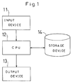
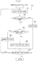
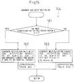
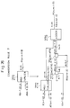
- FIG. 1 is a block diagram showing an example of the hardware structure of an automatic logic-circuit designing system.
- an input device 11 is for inputting functional description information on a circuit to be designed by the automatic designing system.
- the input device 11 can be composed of a keyboard, mouse, light pen, card reader, or schematic entry system. Aside from the foregoing devices that accept the inputting of information through a direct operation by an operator, it can also be composed of a magnetic disk device, which stores information preliminarily inputted through the foregoing devices as a file, or of an network device which receives information sent from another device.
- a CPU 12 is for performing circuit-designing processes such as logical synthesis or circuit optimization by executing a variety of processes, which will be described below.
- An output device 13 is for outputting circuit information which is the result of the designing process by the CPU 12 or a variety of information on processing.
- the output device 13 can be composed of a graphic display, character display, printer, or plotter.
- the output device 13 can also be composed of the magnetic disk device or network device, similarly to the input device 11.
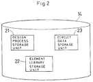
- a storage device 14 consists of, for example, a design process storage unit 21, element library storage unit 22, and circuit data storage unit 23, as shown in FIG. 2, so that it can store information inputted through the input device 11 and programs or data on circuit-designing processes.
- the design process storage unit 21 stores a variety of programs whereby the foregoing CPU 12 executes design processes and conversion rule information to be applied in the course of these processes.
- the element library storage unit 22 stores information on the functions of functional elements, logic elements, and mounted elements and on their area, delay time, and driving forces, so as to provide an element library.
- the circuit data storage unit 23 stores functional description information which is inputted through the input device 11 and functional circuit information, logic circuit information, and mounted circuit information, each of which is generated by the circuit-designing processes.
- the foregoing functional description information is mainly on a function required on a circuit, and is represented in a hardware description language.
- the functional circuit information is mainly on a circuit that is composed of virtual functional elements, the functions of which are only defined, and is represented in an internal representation form.
- the logic circuit information shows a circuit composed of real logic elements, which are on a logic level seldom dependent on the fabrication process or design methods.
- the mounted circuit information is greatly dependent on the fabrication process and design methods and shows a circuit to which are allotted elements actually mounted by a specified technology (e.g., a standard cell composed of a CMOS transistor, a cell in the library of a gate array, or TTL, ECL, and the like which are dependent on the fabrication process).
- a multiple-bit adder represents a functional element for adding two multiple-bit numbers.
- a comparator represents a functional element for comparing two multiple-bit numbers.
- a multiple-bit AND represents a functional element for calculating bit-by-bit logic products of two multiple-bit signals.
- a multiple-bit INV represents a logical element for calculating bit-by-bit logic NOTs in a multiple-bit signal.
- a ripper is a functional element for conveniently dividing a multiple-bit signal during the course of conversion process.
- a mixer is a functional element for conveniently processing the multiple-bit signal as a whole.
- the ripper and mixer are functional elements which are eventually converted to a circuit composed of mounted elements and eliminated when all signals are processed in 1-bit signals.
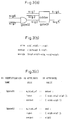
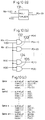
- a circuit composed of, e.g., 1-bit 2-input AND gate and a 1-bit 3-input adder shown in FIG. 3(a) is described in the functional description information shown in FIG. 3(b).
- the functional description information is converted to the functional circuit information or logic circuit information shown in FIG. 3(c).
- the functional circuits information and logic circuit information may not particularly be distinguished from each other in the case shown above where the functional description information corresponds directly to the circuit composed of the functional elements.
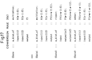
- the functional circuit information includes an identification name 31 for identifying an individual element and a plurality of pairs of attribute code 32 and attribute value 33.
- the attribute code 32 and attribute value 33 in each pair are mapped with " : : “.
- the individual pairs are separated by " ; ", and the identification names 31 are separated from other information by " : : : “.
- the attribute codes 32 include "a_kind_of”, “input”, “output”, and the like, each showing that its corresponding attribute value 33 refers to the type of element, its input signal, and its output signal.
- the element of the gate 01 is an adder, its input signals are sig1, sig2, and sig3, and its output signals are sig4 and sig5.
- the element of the gate 02 is an AND, its input signals are sig6 and sig7, and its output signal is sig3. It is also shown that the gate01 and gate02 are connected by the signal sig3.
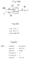
- a circuit composed of a multiplier 51 serving as a functional element, a signal line 52 to which an 8-bit constant having the value of 130 (82h in the hexadecimal notation) is inputted as a multiplier factor, a signal line 53 to which an 8-bit multiplicand a is inputted, and a signal line 54 which outputs a 16-bit multiplication result b, as shown in FIG. 4(a), is described in the functional description information shown in FIG. 4(b), and is converted to the functional circuit information as shown in FIG. 4(c).
- the distinction between the multiplier factor and the multiplicand is provided for the convenience of conversion processes.
- the multiplicand a is a signal having the bit width of 8 ranging from 0 bit to 7 bit.
- the variable b is a signal having the width of 16 ranging from 0 bit to 15 bit. It is shown that the value of the variable b is the product of the multiplicand a and the multiplier factor 130 which is represented by an 8-bit signal having the value of 130.
- the first line shows that the functional element has the identification name of gate1 and it serves as a multiplier.
- the descriptions in the second and fourth lines show that the signal represented by a sign i1 is an 8-bit input signal a having the value of 130.
- the descriptions in the third and fifth lines show that the signal represented by a sign 12 is an 8-bit input signal which is a constant.
- the description in the sixth line shows that the signal represented by a sign o is a 16-bit output signal b.
- a number having the bit width of ( a-b+1 ) ranging from the a-th bit to the b-th bit (a > b) from the least significant digit is designated by X(a : b), while the a-th bit in the number X is designated by X(a).
- posibits Y
- negabits Y
- FIG. 5 is a flow chart showing the main routine of the designing process.
- Step 41 is performed a process of inputting the functional description information formed on the basis of the functional specification by a functional designer of the circuit through the input device 11 and storing it in the circuit data storage unit 23. It is also possible to design the input device 11 so that it accepts the inputting of not only the functional description information but also the functional circuit information and logic circuit information on comparatively simple portions of the circuit.
- Step 42 is performed a process of interpreting the functional description information which was inputted in Step 41, generating functional circuit information in which a circuit consisting of the functional elements and having the function shown in the functional description information is represented in the internal representation form, and storing it in the circuit data storage unit 23.
- Step 43 is performed a process of converting all the functional elements contained in the functional circuit information to logic elements and storing the resulting logic circuit information in the circuit data storage unit 23.
- the circuit including a multiplier the circuit optimization on the level of functional elements is also performed. The process of Step 43 will be described later in detail.
- Step 44 is performed a process of allotting all the logic elements contained in the logic circuit information to mounted elements through the element conversion process based on specified conversion rule information. In this step is also performed circuit optimization on the level of logic elements during the course of allotting the logic elements to the mounted element.
- step 45 is performed a process of generating a circuit diagram and net list based on mounted circuit information and the like and outputting them to the output device 13.
- the net list mentioned above refers to information on, e.g., the connections between the mounted elements in the circuit constituted by the mounted elements.
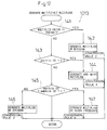
- Step 43 the process shown in detail in FIG. 6 is performed.
- Step 81 one of the functional elements included in the functional circuit information is selected.
- Steps 82 and 83 it is determined whether or not the selected functional element is an adder or a multiplier. If it is an adder, the process goes on to Step 84. If it is a multiplier, the process goes on to Step 85. If it is neither an adder nor a multiplier, the process goes on to Step 86.
- Step 84 to 86 the selected functional element is converted to a circuit having the same function which is constituted by at least either of other functional elements and logic elements. After its circuit information is generated, the process goes on to Step 87.
- Step 87 it is determined whether or not the circuit includes a functional element. If it does, the process goes back to Step 81 so as to repeat the similar processing. If it does not, which means that the circuit obtained by conversion is constituted only by logic circuits, the process returns to the main routine.
- Step 84 to 86 a single conversion process does not necessarily provide a circuit that is constituted only by logic elements. Instead, the circuit resulting from the conversion may temporarily include other functional elements. In this case, it is determined in Step 87 that a functional element is included and, by recursively performing similar conversion processes, a circuit constituted only by logic circuits is eventually obtained. Specifically, a multiple-bit adder is repeatedly converted to an adder having a smaller number of bits (functional element) and to a 1-bit adder (logical element) in Step 84, resulting in a circuit constituted only by 1-bit adders.
- a subtracter and a divider are converted to a circuit composed of functional elements such as adders and of logic circuits in Step 86, and then the functional elements such as adders are converted to 1-bit adders in Step 84.
- the individual processes will easily be simplified.
- the multiplier which is determined as such with "yes" in Step 83 and which is subjected to conversion in Step 85 is provided with the function shown in Figs 7(a) to 7(d).
- the multipliers are the same in that each of them has the function of multiplying a multiplicand represented by an n-bit signal by a multiplier factor represented by an m-bit signal so as to output a product P represented by a signal having the bit width of (n + m).
- the multiplier factor and multiplicand which are inputted thereto are a constant A, constant B, variable X, or variable Y.
- the constant A will be treated as a positive number in the following description.
- the sign of the constant A is inverted so as to generate information on the multiply circuit with respect to the resulting constant A' with the inverted sign and on the circuit for inverting the sign of the multiplication result, thereby providing the proper procedure.
- the variable X may have a positive or negative value.
- Step 85 the conversion process performed in above Step 85 will be described in detail by using a multiplier shown in FIG. 7 in accordance with the flow chart of FIG. 8.
- the process is for converting the multiplier to a circuit constituted by other functional elements such as multipliers and adders or by logic elements.
- Step 1001 If it is determined in Step 1001 that at least either of the multiplier factor or multiplicand is a variable, the process goes on to Step 1003 where it is determined whether or not the multiplicand is a constant, and if the multiplicand is a constant, the multiplier factor and multiplicand are interchanged in Step 1004 so that the process goes on to Step 1005. If the multiplicand is not a constant, on the other hand, the process directly goes on to Step 1005. That is, in the case of using the multiplier shown in Fig. 7(b), it is converted to the multiplier shown in Fig. 7(c) so that at least the multiplicand is constantly a variable.
- Steps 1005, 1007, and 1009 it is determined whether or not the multiplier factor is a special constant, i.e., its value is 0, 1, or a number obtained by raising 2 to a certain power. If the multiplier factor is 0, conversion is made to a circuit for outputting a signal which shows that the values of all the bits are 0, as shown in FIG. 9(b) (Step 1006). If the multiplier factor is 1, conversion is made to a circuit which outputs a signal representing the value of the multiplicand as P(n-1:0), while outputting a signal having the value of X(n-1) as P (n+m-1:n) by sign extension (Step 1008).
- the multiplier factor is a special constant, i.e., its value is 0, 1, or a number obtained by raising 2 to a certain power. If the multiplier factor is 0, conversion is made to a circuit for outputting a signal which shows that the values of all the bits are 0, as shown in FIG. 9(b) (Step 1006). If the multipli
- conversion is made to a circuit which outputs a signal representing the value of the multiplicand as P(n+2:3), outputs a signal having the value of 0 as P(2:0), and outputs a signal in which the value of each bit is X(n-1) as P(n+m-1:n+3) by sign extension, as shown in FIG. 9(d) (Step 1010).
- Step 1011 it is determined whether the multiplier factor is composed of 1 bit or 2 or more bits. If it is composed of 1 bit, as shown in FIG. 10(a), the process goes on to Step 1012, where conversion is made to a circuit composed of AND circuits 132 to 135 as shown in FIG. 10(b).
- the determination of 1 bit in Step 1011 is limited to the case where the multiplier factor is a variable, because, if the multiplier factor is a 1-bit constant, the answers obtained in above Steps 1005 and 1007 must have been 'yes'.
- the determination of 2 or more bits includes the cases where the multiplier factor is a variable and where the multiplier factor is a constant.
- Steps 1006, 1008, 1010, and 1012 conversion to a circuit is performed based on the conversion rule information which is preliminarily stored in the design process storage unit 21.
- the conversion of step 1012 is performed based on conversion rule 1 shown in FIG. 10(c) by following the process shown in FIG. 11.
- Step 72 the circuit information on the initial multiplier as a functional element is deleted from the circuit data storage unit 23.
- Step 74 it is determined whether or not unprocessed functional or logic elements remain in the condition clause. If the answer is yes, the process goes back to above Step 73. If the answer is no, on the contrary, the process returns to the initial process.
- Step 1011 If it is determined that the multiplier factor is composed of 2 or more bits in above Step 1011, the process goes on to Step 1013, where conversion is made to a multiple-bit multiplier composed of at least either of other functional elements (multiplier or adder having a reduced bit width) and logic elements.
- FIG. 12 is a flow chart showing the process performed in above Step 1013 in detail. In the process, the number of partial products and the number of logic stages for calculating the sum of the partial products are mostly reduced in the following manner.
- the multiplier factor is a constant
- conversion is made to a circuit which calculates a partial product only with respect to a bit having the value of 1 in the multiplier factor or in a logic NOT number which is obtained by inverting all the bits in the multiplier factor by the logic NOT operation, thereby reducing the number of the partial products.
- conversion is made to a circuit in which an adder is connected so as to form a binary tree, thereby reducing the number of logic stages in the circuit for calculating the sum of the partial products.
- Step 141 it is determined whether or not the multiplier is a variable or not. If the answer is yes, it follows that multiplication will be performed by using variables as its multiplier factor and multiplicand, so that the process goes on to Step 142.
- Step 142 conversion is made, according to conversion rule 2, to a circuit including two multipliers in which the multiplier factor having the bit width of about 1/2 is used.
- a multiplier 191 which outputs a product P by multiplying an n-bit multiplicand X by an m-bit multiplier factor Y, is converted to a circuit consisting of multipliers 192 and 193, which calculates partial products P1 and P2 by multiplying the multiplicand X by the low-order K bits and high-order (m-K) bits of the multiplier factor Y, respectively, and of a circuit for adding the resulting partial products P1 and P2.
- the foregoing circuit since it is sufficient for the foregoing circuit to perform addition only with respect to the overlapping bit of the partial products P1 and P2 and to the bits higher than the overlapping bit, it is constituted by a ripper 194 for separating the high-order n bits of the partial product P1 from its low-order K bits, mixer 195 for outputting a signal R1 obtained by extending the sign of the high-order n bits, and an adder 196 for adding the signal R1 and the partial product P2.
- the ripper 194 is a circuit for dividing the foregoing signal P1 (n+K-1:0) into a signal P1 (n+K-1:K) composed of the high-order n bits and a signal P1 (K-1:0) composed of the low-order K bits.
- the latter signal P1 (K-1:0) is outputted as a signal P (K-1:0) representing the low-order K bits of the product P.
- the mixer 195 is a circuit for gathering a signal having the bit width of (m-K), in which the value of each bit is P1 (n+K-1) , in the high order of the signal P1 (n+K-1:K) and for outputting a signal R1 (n+m-K-1:0) having the bit width of ( n+m-K ) by extending the sign of the signal P1.
- the adder 196 is a circuit for adding the foregoing signal P2 (n+m-K-1:0) and the signal R1 (n+m-K-1:0) and for outputting a signal R2 (n+m-K-1:0) having the bit width of ( n+m-K ), which is the sum of the foregoing signals, as a signal P (n+m-1:K) representing the high-order ( n+m-K ) bits of the product P.
- the value of above K is set to the minimum integer equal to or more than m/2 or to the maximum integer equal to or less than m/2, that is, to an integer which minimizes the absolute value of the difference (m-2K) between K and (m-K).
- the value of above K is set so that the either K or (m-K) becomes the minimum value obtained by raising 2 to a certain power that is equal to or more than m/2.
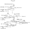
- FIG. 14 is a view showing the structure for performing the process of above Step 142 in terms of its function.
- an input means 241 reads the circuit information on the initial multiplier 191 as a functional element out of the circuit data storage unit 23, and then outputs, to a means 242 for dividing multiplier factor, the information which shows that the inputs to the multiplier 101 are the m-bit multiplier factor Y and the n-bit multiplicand X.
- the input means 241 also outputs, to a means 244 for generating division calculating circuit, the information which shows that the output from the multiplier 191 is the product P having the bit width of (m+n).
- the means 242 for dividing multiplier factor initially calculates the value of K for dividing the multiplier factor Y, and then outputs, to a means 243 for generating multiplication module, information on the signal Y1 composed of the low-order K bits of the multiplier factor Y, multiplicand X, and partial product P1 and information on the signal Y2 composed of the high-order (m-K) bits of the multiplier factor Y, multiplicand X, and partial product P2.
- the means 242 for dividing multiplier factor also outputs respective sets of information on the partial products P1 and P2 to the means 244 for generating division calculating circuit.
- the names P1 and P2 of the foregoing partial products are allotted here by an allotting means (not shown).
- the means 243 for generating multiplication module generates information on the multiplier 192 which multiplies the multiplicand X by the signal Y1 so as to obtain the partial product P1 and on the multiplier 193 which multiplies the multiplicand X by the signal Y2 so as to obtain the partial product P2, and then outputs the resulting information to an output means 245.
- the means 244 for generating division calculating circuit outputs, to the output means 245, information on a circuit consisting of a ripper 194, mixer 195, and adder 196, which outputs, based on information on the partial products P1 and P2 and information on the product P, the low-order K bits of the partial product P1 as the low-order K bits of the product P while outputting the sum of the high-order (n-K) bits of the partial product P1 and partial product P2 as the high-order ( n+m-K ) bits of the product P.
- the output means 245 stores the circuit information on the circuit obtained by conversion, which was outputted from the means 243 for generating multiplication module and from the means 244 for generating division calculating means.
- multiplier which performs multiplication by using variables as its multiplier factor and multiplicand
- conversion is not limited to the foregoing process that involves division. It is also possible to allot thereto a general purpose multiplier entered in the library or to convert it to a circuit using the 2-bit Booth's recode system, similarly to the conventional automatic designing system.
- Step 141 if it is determined that the multiplier factor is a constant multiplier factor A, the process goes on to Step 143, where it is determined whether or not the posibits (A), which indicates the number of bits having the value of 1 in the multiplier factor A, is 2 or less. If the posibits (A) is 2 or less, the process goes on to Step 144. If the posibits (A) is 1, it must have been processed in above Step 1008 or 1010, so that the determination of 2 or less is limited to the case where the posibits (A) is 2. In Step 143, the value of m may also be determined.
- Such a circuit may be formed by a single process, but in this case, conversion is made to a circuit having a (m-1)-bit multiplier which divides the multiplier factor A into the most significant 1 bit and the low-order (m-1) bits, while adding the product of the multiplicand X and the low-order (m-1) bits of the multiplier factor A and the value obtained by shifting the multiplicand X, so that recursive processing simplifies individual processes.
- the most significant bit of the multiplier factor A is 0, it is sufficient to set the most significant bit of the product P to 0, so that the circuit for performing addition or the like is not necessary.
- Step 144 it is initially determined in Step 161 whether or not the most significant bit of the multiplier factor A is 1. If it is 1, the process goes on to Step 162, where conversion rule 3(a) shown in FIG. 16(a) is applied. Conversely, if it is 0, the process goes on to Step 163, where conversion rule 3(b) shown in FIG. 16(b) is applied.
- the conversion rule 3(a) and conversion rule 3(b) constitute conversion rule 3.
- a multiplier 151 is converted to a circuit consisting of a multiplier 152, ripper 153, and adder 154.
- the ripper 153 divides the partial product P3 into the high-order n bits P3 (n+m-2:m-1) and the low-order (m-1) bits P3 (m-2:0).
- the adder 154 adds the foregoing P3 (n+m-2:m-1) and the multiplicand X (n-1:0) (logically, the product of the most significant bit of the multiplier factor A and the multiplicand X (n-1:0) as a partial product).
- the multiplier 151 can be converted to a circuit including the multiplier having a reduced bit width without increasing the number of the partial products.
- Step 144 is executed again in the process of the next loop and conversion is made to a circuit which includes a multiplier having a further reduced bit width in Step 163, or conversion is made to a circuit which includes a multiplier having one bit the value of which is 1 in Step 162.
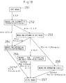
- FIG. 18 is a view showing the structure for performing the process of above Step 144 in terms of its function.
- an input means 251 reads the circuit information on the initial multiplier 151 as an functional element out of the circuit data storage unit 23 and outputs, to a means 252 for separating the most significant bit, information which shows that the inputs to the multiplier 151 are the m-bit multiplier factor A and the n-bit multiplicand X and that the output from the multiplier 151 is the product P having the bit width of (m+n).
- the means 252 for separating the most significant bit separates the most significant bit A (m-1) of the multiplier factor A from the low-order bits A (m-2:0) thereof and outputs, to a means 253 for determining bit value, information on the most significant bit A (m-1), multiplicand X, and product P, while outputting, to a means 254 for generating multiplication module, information on the lower bits A (m-2:0) and multiplicand X.
- the means 253 for determining bit value determines whether the value of the most significant bit A (m-1) is 1 or 0 and outputs, to the means 254 for generating multiplication module, the information showing that the result of multiplying the multiplicand X by the low-order bits A (m-2:0) is the partial product P3 or the product P (n+m-2:0) , depending on the result of determination. If the value of the most significant bit A (m-1) is 1, information on the multiplicand X, product P, and partial product P3 is outputted to a means 255 for generating add shift calculating circuit. Conversely, if the value of the most significant bit A (m-1) is 0, information on the most significant bit P (n+m-1) of the product P and information on the value P (n+m- 2) is outputted to a means 256 for generating circuit.
- the means 254 for generating multiplication module generates information on the multipliers 152 and 155 which multiply the multiplicand X by the low-order bits A (m-2:0) of the multiplier factor A so as to output the result as the partial product P3 or product P (n+m-2:0) , and outputs the resulting information to an output means 257.
- the means 255 for generating add shift calculating circuit generates information on a circuit consisting of the ripper 153 and adder 154, which outputs, in the case where the value of the most significant bit A (m-1) of the multiplier factor A is 1, the low-order (m-1) bits of the partial product P3 as the low-order (m-1) bits P (m-2:0) of the product P, while outputting the sum of the high-order n bits of the partial product P3 and multiplicand X as the high-order (n+1) bits P (n+m-1:m-1) of the product P, based on information on the partial product P3, information on the multiplicand X, and information on the product P.
- the resulting information is then outputted to the output means 257.
- the means 256 for generating circuit generates information on a circuit, which outputs, in the case where the value of the most significant bit of the multiplier factor A is 0, the value P (n+m-2) as the most significant bit P (n+m-1) of the product P.
- the resulting information is outputted to the output means 257.
- the output means 257 stores in the circuit data storage unit 23 the sets of circuit information on the circuit obtained by conversion, which are outputted from the respective means 254 to 256.
- Step 143 If it is determined in above Step 143 that the posibits (A) in the constant multiplier factor A is more than 2, the process goes on to Step 145, where it is further determined whether or not the posibits (A) is larger than the negabits (A)+1.
- the negabits (A) indicates the number of bits having the value of 0.
- Step 145 if it is determined that the posibits (A) is not larger than the negabits (A)+1, the process goes on to Step 146.
- Step 146 the conversion rule 2 shown in FIG. 13 is applied, similarly to the case of above Step 142 where the multiplier factor is a variable, so as to divide the multiplier factor A and conversion is made to a circuit including two multipliers.
- the value of K for dividing the multiplier factor A used here is not about 1/2 of the bit width of the multiplier factor A. Instead, the value of effbitwidth (A, L) is used.
- the effbitwidth (A, L) is defined as a value obtained by calculating the number of bits having the value of 1 from the least significant bit of the multiplier factor A till it becomes L, if L is the minimum integer equal to or more than the posibits (A)/2.
- the value of above L may be the maximum integer equal to or less than the posibits (A)/2 or a number obtained by raising 2 to a certain power which is close to the maximum integer, similarly to the value of above K.
- the number of logic stages always becomes 2 no matter how the multiplier factor A is divided. Therefore, it is also possible to determine whether or not the posibits (A) is 3 or less in Step 143, and to divide the multiplier factor A into the most significant 1 bit and the low-order (m-1) bits in Step 144, if the posibits (A) is 3.
- the structure for performing the process of above Step 146 is the same as the structure of FIG. 14 corresponding to above Step 142, except that the manners to determine the value of K for dividing the multiplier factor A are different.
- Step 147 where conversion rule 4 shown in FIG. 19 is applied so that conversion is made to a circuit including a multiplier for obtaining the product of a multiplier factor A0, which is obtained by inverting all the bits in the multiplier factor A by the logic NOT operation, and the multiplicand X.
- the multiplier included in the circuit after conversion the value of the posibits (A) and the value of the negabits (A) are switched, so that in the process of the next loop, the answer obtained in Step 145, for example, becomes "no", resulting in conversion whereby the multiplier A0 is divided in Step 146.
- the circuit for obtaining partial products only with respect to the bits having the value of 0 is produced while the number of bits having the value of 1 is reduced compared with that of the multiplier factor A, so that the number of circuits for calculating the partial products and the number of logic stages in the circuits for calculating the sum of the partial products are reduced.
- numeral 171 denotes a multiplier prior to conversion.
- An inverter 178 inverts all the bits in the product PO by the logic NOT operation and outputs a signal having the bit width of (n+m).
- the mixer 174 gathers a signal by using an m-bit signal in which each bit has the value X (n-1), which is the value of the most significant bit of the multiplicand X as its high-order m bits and the logic NOT number of the foregoing multiplicand X as its low-order n bits, so as to outputs the resulting signal having the bit width of (n+m).
- Step 145 The requirement on determination in above Step 145 is not limited to: posibits (A) > negabits (A)+1. It can be: posibits (A) ⁇ m/2 or the like. In consideration of the sizes of the individual circuits for the foregoing correction, it is also possible for the process to go on to Step 147 only when the value of posibits (A) is larger.
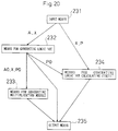
- FIG. 20 is a view showing the structure for performing the process of above Step 147 in terms of its function.
- An input means 231 reads circuit information on the initial multiplier 171 as a functional element out of the circuit data storage unit 23 and outputs, to a means 232 for generating logic NOT, information which shows that the inputs to the multiplier 171 is the m-bit multiplier factor A and n-bit multiplicand X.
- the input means also outputs, to a means 234 for generating logic NOT calculating circuit, information on the foregoing multiplicand X and information which shows that the output from the multiplier 171 is the product P having the bit width of (m+m).
- the means 232 for generating logic NOT outputs, to a means 233 for generating multiplication module, information on an inverter 179 for outputting the multiplier factor A0 by inverting all the bits in the multiplier factor A by the logic NOT operation, information on the foregoing multiplier factor A0, information on the multiplicand X, and information which shows that the result of multiplying the multiplicand X by the multiplier factor A0 is a product P0.
- the means 232 for generating logic NOT also outputs, to the means 234 for generating logic NOT calculating circuit, information on the foregoing product P0.
- the means 233 for generating multiplication module generates information on a multiplier 172 for calculating the product P0 of the multiplier factor A0 and multiplicand X and outputs it to an output means 235.
- the output means 235 stores in the circuit data storage unit 23 circuit information on the circuit after conversion, which was outputted from the means 232 to 234.
- numeral 132 denotes an AND circuit for calculating a logic product P(n-1) of a 1-bit multiplicand X(n-1) and a 1-bit variable multiplier factor Y(0)
- numeral 133 denotes an AND circuit for calculating a logic product P(n-2) of a 1-bit multiplicand X(n-2) and a 1-bit variable multiplier factor Y(0)
- numeral 134 denotes an AND circuit for calculating a logic product P(1) of a 1-bit multiplicand X(1) and a 1-bit variable multiplier factor Y(0)
- the second term X can be obtained as R3 by the mixer 174 and inverter 177 through sign extension and inversion of all the bits by the logic NOT operation.
- the fourth term P0 can be obtained by the multiplier 172 and inverter 178.
- the addition of the first term X * 2 m , second term X, and 1 as the third term or fifth term can be performed by the adder 175, thus providing the sum R4. Since X * A is a number having the bit width of (n+m), it is not necessary to consider the ( n+m+1 )-th bit position in the addition result.
- the multiplier factor inputted to the multiplier is a constant and if the total number of bits having the value of 1 is 3 or more, the multiplier factor is divided into two parts so that each part includes the equal number of bits having the value of 1. Consequently, the circuit for calculating the sum of the partial products is structured in a well-balanced binary tree, and it becomes possible to reduce the number of logic stages and provide higher-speed multiplication.
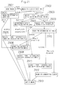
- an input means 2901 reads circuit information on the initial multiplier as functional element out of the circuit data storage unit 23 and outputs, to a means 2902 for judging logic NOT 2902, information which shows that the inputs to the multiplier are the m-bit multiplier factor A or Y and the n-bit multiplicand X and that the output from the multiplier is the product P having the bit width of (m+n).
- the means 2902 for judging logic NOT judges whether or not the posibits (A) is larger than the negabits (A)+1. If the answer is yes, information on the multiplier factor A or Y, multiplicand X, and product P is outputted to a means 2904 for generating logic NOT. Conversely, if the answer is no, the foregoing information is outputted to a means 2903 for determining the bit width of multiplier factor.
- the means 2903 for determining the bit width of multiplier factor determines whether or not the multiplier factor is a variable, whether or not the multiplier factor is a constant and the posibits (A) is 3 or more, or whether or not the multiplier factor is a constant and the posibits (A) is 2 or less.
- the multiplier factor is a variable or when the multiplier factor is a constant and the posibits (A) is 3 or more, the information on the multiplier factor A or Y, multiplicand X, and product P is outputted to a means 2907 for dividing multiplier factor.
- the multiplier factor is a constant and the posibits (A) is 2 or less, the information on the multiplier factor A or Y, multiplicand X, and product P is outputted to a means 2909 for separating the most significant bit of multiplier.
- the multiplier factor is divided into two parts so that each part has the bit width of about 1/2, whether the multiplier factor is a constant or variable. If the bit width of the multiplier factor is 2 and if the multiplier factor is a constant, the foregoing conversion rule 3 (see FIGS 16(a) and 16(b)) is applied, so that conversion is made to a circuit for calculating partial products only with respect to the bits having the value of 1. On the other hand, if the multiplier factor is a variable, a circuit including two multipliers which use a 1-bit multiplier factor is constituted.
- Step 211 it is determined whether the bit width of the multiplier factor is 3 or more. If it is 3 or more, the process goes on to Step 212, where the foregoing conversion rule 2 (see FIG. 13) is applied so that conversion is made to a circuit including two multipliers in which the bit width of the multiplier factor is about 1/2.
- Step 213 If the bit width of the multiplier factor is less than 3, the process goes on to Step 213, where it is determined whether or not the multiplier factor is a constant. If it is a constant, the process goes on to Step 214, where the foregoing conversion rule 3 (see FIGS. 16(a) and 16(b)) is applied so that conversion is made to a circuit for calculating partial products only with respect to the bits having the value of 1 in the multiplier factor.
- Step 215 the process goes on to Step 215, where conversion rule 5 shown in FIG. 23 is applied.
- the conversion rule 5 shows that a multiplier 221 is converted to a circuit consisting of multipliers 222 and 223, ripper 224, mixer 225, and adder 226.
- the foregoing multiplier 222 multiplies the multiplicand X(n-1:0) by the low-order 1 bit A(0) of the multiplier factor A (1:0), so as to calculate the partial product R1(n:0) having the bit width of (n+1).
- the multiplier 223 multiplies the multiplicand X(n-1:0) by the high-order 1 bit A(1) of the multiplier factor A (1:0), so as to calculate the partial product R2 (n+1:1) having the bit width of (n+1).
- the ripper 224 divides the partial product R1(n:0) into the high-order n bits R1(n:1) and the low-order 1 bit R(0), so as to output R(0) as the product P(0).
- the mixer 225 outputs a signal R3(n+1:1) which is obtained by extending the sign of above R1(n:1) by 1 bit to the higher order.
- the adder 226 adds the signal R3(n+1:1) and partial product R2(n+1:1) so as to output the sum R4(n+1:1) as the product P(n+1:1).
- the bit width of the multiplier factor in the multiplier is 3 or more, it becomes possible to structure the circuit for calculating partial products in a binary tree by dividing the multiplier factor, so that the number of logic stages in multiplication can be reduced and the speed of multiplication can be increased.
- the bit width of the multiplier factor is 2 or less and if the multiplier factor is a constant, it becomes possible to reduce the number of partial products and circuit area by generating the circuit for calculating partial products only with respect to the bits having the value of 1 in the multiplier factor.
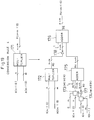
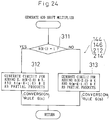
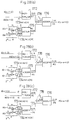
- Step 311 it is determined whether or not the value of the K-th bit A(K-1) in the multiplier factor A is 1 in Step 311. If it is 1, the process goes on to Step 312, where conversion rule 6(a) shown in FIG. 25(a) is applied. On the other hand, if it is 0, the process goes on to Step 313, where conversion rule 6(b) shown in FIG. 25(b) is applied.
- the conversion rules 6(a) and 6(b) constitute the conversion rule 6.
- the value of above K it can be set similarly to that of, e.g., the first embodiment.
- the conversion rule 6(a) shows that a multiplier 281 is converted to a circuit consisting of multipliers 282 and 283, mixers 284 to 287, and adder 288.
- the mixer 284 outputs a signal R1(n+m-1:0) which is obtained by extending the sign of the partial product P5(n+K- 2:0) by ( m-K+1 ) bits to the higher order.
- the mixer 285 outputs a signal R2(n+m-1:0) which is a K-bit signal having the value of 0 gathered in the lower order of the partial product P6.
- the mixer 286 outputs a signal R3(n+K-2:0) which is obtained by gathering a signal having the value of 0 and the bit width of (K-1) in the lower order of the multiplicand X(n-1:0).
- the mixer 287 outputs a signal R4(n+m-1:0) which is obtained by extending the sign of the foregoing signal R3(n+K-2:0) by ( m-K+1 ) bits to the higher order.
- the adder 288 adds the foregoing signal R1(n+m-1:0) , signal R2(n+m-1:0) , and signal R4(n+m-1:0) so as to output the product P(n+m-1:0) .
- the conversion rule 6(b) shows that the multiplier 281 is converted to a circuit consisting of the multipliers 282 and 283, mixers 284 and 287, and an adder 289.
- the foregoing adders 282 and 283 and mixers 284 and 287 are the same as shown in the conversion rule 6(a).
- the adder 289 adds the signal R1(n+m-1:0) and signal R2(n+m-1:0) so as to output the product P(n+m-1:0) .
- the conversion rule 7 shows that a multiplier 271 is converted to a circuit consisting of a multiplier 272, mixers 273 and 274, and adder 275.
- the multiplier 272 multiplies the multiplicand X by an m-bit multiplier factor A7 (m-1:0) which is obtained by setting the K-th bit ( 0 ⁇ K ⁇ m-1 ) having the value of 1 in the multiplier factor A(m-1:0) to 0, so as to output the product P7(n + m - 1 : 0) .
- the mixer 273 gathers a signal by using the multiplicand X as the high-order n bits and by using a signal having the value of 0 and the bit width of (K-1) as the low-order (K-1) bits and outputs the resultant signal R1(n+K-2:0) having the bit width of ( n+K-1 ).
- the mixer 274 gathers a signal having the bit width of ( m-K+1 ) in which each bit has the value of R1(n+k-2) in the higher order of the foregoing signal R1(n+K-2:0) by extending the sign of the signal R1 and outputs the resulting signal R2(n+m-1:0) having the bit width of (n+m).
- the adder 275 adds the product P7(n+m-1:0) and signal R2(n+m-1:0) , so as to output the sum R3(n+m-1:0) as the product P(n+m-1:0) .
- bit width of the multiplier factor A7(m-1:0) inputted to the multiplier 272 is equal to the bit width of the multiplier factor A (m-1:0) inputted to the multiplier 271.
- the process of above Step 1008 or Step 1010 will eventually be implemented.
- FIG. 27 is a view showing the structure for performing the foregoing conversion rule 7 in terms of its function.
- An input means 261 reads circuit information on the initial multiplier as a functional element out of the circuit data storage unit 23 and outputs information, to a means 262 for generating signal, information which shows that the inputs to the multiplier 271 are the m-bit multiplier factor A and n-bit multiplicand X.
- the input means 261 also outputs, to a means 264 for generating calculating circuit, information on the multiplicand X and information which shows that the output from the multiplier 271 is the product P having the bit width of (m+n).
- the means 262 for generating signal outputs, to a means 263 for generating calculation module, information on a multiplier factor A7 which is obtained by turning the K-th bit ( 0 ⁇ K ⁇ m-1 ), having the value of 1, in the multiplier factor A to 0, information on the multiplicand X, and information which shows that the multiplication result is a product P7.
- the means 262 for generating signal also outputs information on the value of above K and information on the product P7 to the means 264 for generating calculating circuit.
- the means 263 for generating calculation module generates information on the multiplier 272 for calculating the product P7 of the foregoing signal X and signal A7 and outputs the resulting information to an output means 265.
- the means 264 for generating calculating circuit outputs, based on the information on the value of K, the information on the product P7, information on the multiplicand X, and information on the product P, information on mixers 276 and 274 and on a multiplier 275 to the output means 265.
- the output means 265 stores in the circuit data storage unit 23 circuit information on the circuit obtained by conversion, which was outputted from the means 263 for generating multiplication module and from the means 264 for generating calculating circuit.
- variable X is a positive number for simplicity, if the variable X can be a positive or negative number, it is possible to calculate the logic NOT number after sign extension, similarly to the conversion 4, or to perform sign extension after calculating the logic NOT number.
- FIGS. 28(a) to 28(c) show the conclusion clauses of the conversion rules as well as the structures of multipliers generated. Since the components shown in FIGS. 28(a) to 28(c) are the same as shown in FIG. 19, the description thereof will be omitted by providing the same numerals.
- a signal having the value of 1 is inputted to the mixer 173 as an m-bit signal instead of a signal having the value of 1 being inputted to the multiplier 175 as a carry.
- a signal having the value of 1 is inputted to the mixer 173 as an m-bit signal instead of a signal having the value of 1 being inputted to the multiplier 176 as a carry.
- bit width m of the multiplier factor is 2 or more, it is possible to input a signal having the value of 2 to the mixer 17 as an m-bit signal, instead of inputting a signal having the value of 1 as a carry, as shown in FIG. 28(c).
- the calculation for obtaining the product P by correcting the product P0 can be modified in various manners.
- any multiplier included therein is designed to multiply the multiplicand X by the multiplier factor A0, which is the value obtained by inverting all the bits in the multiplier A by the logic NOT operation. Consequently, even when posibits (A) is larger than m/2, it is possible to reduce circuit area and increase the speed of multiplication by reducing the number of partial products to m/2 or less.
- circuit information stored in the circuit data storage unit 23 has been described in information representation which represents circuits in terms of functional elements, logic elements, and mounted elements, and more specifically, in terms of inputs and outputs to and from these elements.
- the present invention is not limited thereto, and it is also possible to perform a process of converting circuits in accordance with similar conversion rules, even if information representation based on the relationships among the elements, namely signals, is used instead.
- the conversion process is not limited to the process of converting circuits in accordance with the foregoing conversion rules, either.
- the conversion process can be a process of sequentially generating and entering parts of circuit information in a specified order.
- the product P of the m-bit multiplier factor and n-bit multiplicand has the bit width of (n+m)
Landscapes
- Engineering & Computer Science (AREA)
- Physics & Mathematics (AREA)
- General Physics & Mathematics (AREA)
- Theoretical Computer Science (AREA)
- Mathematical Optimization (AREA)
- Pure & Applied Mathematics (AREA)
- Mathematical Analysis (AREA)
- Computational Mathematics (AREA)
- General Engineering & Computer Science (AREA)
- Computing Systems (AREA)
- Computer Hardware Design (AREA)
- Evolutionary Computation (AREA)
- Geometry (AREA)
- Complex Calculations (AREA)
- Design And Manufacture Of Integrated Circuits (AREA)
Applications Claiming Priority (3)
| Application Number | Priority Date | Filing Date | Title |
|---|---|---|---|
| JP348269/92 | 1992-12-28 | ||
| JP4348269A JP2840169B2 (ja) | 1992-12-28 | 1992-12-28 | 論理回路の自動設計方法およびその装置 |
| JP34826992 | 1992-12-28 |
Publications (3)
| Publication Number | Publication Date |
|---|---|
| EP0605885A2 true EP0605885A2 (fr) | 1994-07-13 |
| EP0605885A3 EP0605885A3 (fr) | 1995-05-10 |
| EP0605885B1 EP0605885B1 (fr) | 2003-04-02 |
Family
ID=18395900
Family Applications (1)
| Application Number | Title | Priority Date | Filing Date |
|---|---|---|---|
| EP93121019A Expired - Lifetime EP0605885B1 (fr) | 1992-12-28 | 1993-12-28 | Méthode et appareil pour la conception automatique de circuit logique et multiplicateur |
Country Status (5)
| Country | Link |
|---|---|
| US (2) | US5530664A (fr) |
| EP (1) | EP0605885B1 (fr) |
| JP (1) | JP2840169B2 (fr) |
| KR (1) | KR970006408B1 (fr) |
| DE (1) | DE69332817T2 (fr) |
Cited By (2)
| Publication number | Priority date | Publication date | Assignee | Title |
|---|---|---|---|---|
| EP0642093A2 (fr) * | 1993-09-02 | 1995-03-08 | Matsushita Electric Industrial Co., Ltd. | Procédé et dispositif pour la conception automatique d'un circuit multiplicateur |
| GB2492488A (en) * | 2011-06-30 | 2013-01-02 | Imagination Tech Ltd | A logic circuit performing a multiplication as the sum of addends operation with a desired rounding precision |
Families Citing this family (9)
| Publication number | Priority date | Publication date | Assignee | Title |
|---|---|---|---|---|
| JP2972540B2 (ja) * | 1994-03-24 | 1999-11-08 | 松下電器産業株式会社 | Lsi自動設計システム及びlsi自動設計方法 |
| US5815422A (en) * | 1997-01-24 | 1998-09-29 | Vlsi Technology, Inc. | Computer-implemented multiplication with shifting of pattern-product partials |
| US6718465B1 (en) * | 2000-02-25 | 2004-04-06 | The Research Foundation Of State University Of New York | Reconfigurable inner product processor architecture implementing square recursive decomposition of partial product matrices |
| US6978426B2 (en) * | 2002-04-10 | 2005-12-20 | Broadcom Corporation | Low-error fixed-width modified booth multiplier |
| US6971083B1 (en) * | 2002-11-13 | 2005-11-29 | Altera Corporation | Method for programming programmable logic device with blocks that perform multiplication and other arithmetic functions |
| US7395300B2 (en) * | 2004-01-27 | 2008-07-01 | Broadcom Corporation | System, and method for calculating product of constant and mixed number power of two |
| US7380226B1 (en) * | 2004-12-29 | 2008-05-27 | Cadence Design Systems, Inc. | Systems, methods, and apparatus to perform logic synthesis preserving high-level specification |
| US7912891B2 (en) * | 2005-12-09 | 2011-03-22 | Electronics And Telecommunications Research Institute | High speed low power fixed-point multiplier and method thereof |
| US10289259B2 (en) * | 2007-02-13 | 2019-05-14 | Visual Targeting Corporation | Method for defining a presentation format targetable to a demographic |
Citations (2)
| Publication number | Priority date | Publication date | Assignee | Title |
|---|---|---|---|---|
| FR2650088A1 (fr) * | 1989-07-18 | 1991-01-25 | Thomson Csf | Procede pour la generation de schemas logiques de circuits multiplieurs parametrables a decodeur de booth au moyen d'un ordinateur et circuits multiplieurs correspondants |
| EP0437876A1 (fr) * | 1989-12-15 | 1991-07-24 | Laboratoires D'electronique Philips S.A.S. | Multiplieur série programmable |
Family Cites Families (10)
| Publication number | Priority date | Publication date | Assignee | Title |
|---|---|---|---|---|
| JPS5164844A (fr) * | 1974-12-03 | 1976-06-04 | Fujitsu Ltd | |
| US4964056A (en) * | 1987-03-25 | 1990-10-16 | Hitachi, Ltd. | Automatic design system of logic circuit |
| JP2877303B2 (ja) * | 1987-03-31 | 1999-03-31 | 株式会社東芝 | 集積回路の自動設計装置 |
| JPH0315984A (ja) * | 1987-09-25 | 1991-01-24 | Matsushita Electric Ind Co Ltd | 機能記述変換方法と論理設計システム |
| JP2506991B2 (ja) * | 1987-09-25 | 1996-06-12 | 松下電器産業株式会社 | 回路変換システムと回路変換方法と反転論理生成方法および論理設計システム |
| KR920003908B1 (ko) * | 1987-11-19 | 1992-05-18 | 미쓰비시뎅끼 가부시끼가이샤 | 승산기(乘算器) |
| JP2682142B2 (ja) * | 1989-06-14 | 1997-11-26 | 松下電器産業株式会社 | 乗算装置 |
| JP2563663B2 (ja) * | 1990-08-20 | 1996-12-11 | 松下電器産業株式会社 | 論理設計処理装置およびタイミング調整方法 |
| US5345393A (en) * | 1990-08-22 | 1994-09-06 | Matsushita Electric Industrial Co., Ltd. | Logic circuit generator |
| US5351206A (en) * | 1992-11-12 | 1994-09-27 | Vlsi Technology, Inc. | Signed two's complement constant multiplier compiler |
-
1992
- 1992-12-28 JP JP4348269A patent/JP2840169B2/ja not_active Expired - Fee Related
-
1993
- 1993-12-20 KR KR1019930028580A patent/KR970006408B1/ko not_active IP Right Cessation
- 1993-12-28 DE DE69332817T patent/DE69332817T2/de not_active Expired - Fee Related
- 1993-12-28 US US08/174,450 patent/US5530664A/en not_active Expired - Lifetime
- 1993-12-28 EP EP93121019A patent/EP0605885B1/fr not_active Expired - Lifetime
-
1996
- 1996-03-21 US US08/620,046 patent/US5703802A/en not_active Expired - Fee Related
Patent Citations (2)
| Publication number | Priority date | Publication date | Assignee | Title |
|---|---|---|---|---|
| FR2650088A1 (fr) * | 1989-07-18 | 1991-01-25 | Thomson Csf | Procede pour la generation de schemas logiques de circuits multiplieurs parametrables a decodeur de booth au moyen d'un ordinateur et circuits multiplieurs correspondants |
| EP0437876A1 (fr) * | 1989-12-15 | 1991-07-24 | Laboratoires D'electronique Philips S.A.S. | Multiplieur série programmable |
Non-Patent Citations (1)
| Title |
|---|
| IEEE INTERNATIONAL CONFERENCE ON COMPUTER-AIDED-DESIGN, 11 November 1991, SANTA CLARA US pages 106 - 109 ARTS ET AL 'flexible block-multiplier generation' * |
Cited By (6)
| Publication number | Priority date | Publication date | Assignee | Title |
|---|---|---|---|---|
| EP0642093A2 (fr) * | 1993-09-02 | 1995-03-08 | Matsushita Electric Industrial Co., Ltd. | Procédé et dispositif pour la conception automatique d'un circuit multiplicateur |
| EP0642093A3 (fr) * | 1993-09-02 | 1996-03-13 | Matsushita Electric Ind Co Ltd | Procédé et dispositif pour la conception automatique d'un circuit multiplicateur. |
| US5600569A (en) * | 1993-09-02 | 1997-02-04 | Matsushita Electric Industrial Co., Ltd. | Method, system, and apparatus for automatically designing logic circuit, and multiplier |
| EP1475699A2 (fr) * | 1993-09-02 | 2004-11-10 | Matsushita Electric Industrial Co., Ltd. | Multiplieur |
| EP1475699A3 (fr) * | 1993-09-02 | 2004-11-17 | Matsushita Electric Industrial Co., Ltd. | Multiplieur |
| GB2492488A (en) * | 2011-06-30 | 2013-01-02 | Imagination Tech Ltd | A logic circuit performing a multiplication as the sum of addends operation with a desired rounding precision |
Also Published As
| Publication number | Publication date |
|---|---|
| EP0605885A3 (fr) | 1995-05-10 |
| US5703802A (en) | 1997-12-30 |
| KR970006408B1 (ko) | 1997-04-28 |
| JPH06203098A (ja) | 1994-07-22 |
| DE69332817D1 (de) | 2003-05-08 |
| US5530664A (en) | 1996-06-25 |
| EP0605885B1 (fr) | 2003-04-02 |
| KR940015785A (ko) | 1994-07-21 |
| JP2840169B2 (ja) | 1998-12-24 |
| DE69332817T2 (de) | 2003-11-06 |
Similar Documents
| Publication | Publication Date | Title |
|---|---|---|
| EP0642093B1 (fr) | Procédé, système et dispositif pour la conception automatique d'un circuit multiplicateur et circuit multiplicateur conçu par la mise en oeuvre dudit procédé | |
| JP3244506B2 (ja) | 小型乗算器 | |
| JP2000259394A (ja) | 浮動小数点乗算器 | |
| US5184318A (en) | Rectangular array signed digit multiplier | |
| US5367477A (en) | Method and apparatus for performing parallel zero detection in a data processing system | |
| US5703802A (en) | Method and apparatus for automatically designing logic circuit, and multiplier | |
| GB2239536A (en) | Binary division of signed operands | |
| US5144576A (en) | Signed digit multiplier | |
| US5903470A (en) | Method and apparatus for automatically designing logic circuit, and multiplier | |
| US4805131A (en) | BCD adder circuit | |
| US5289399A (en) | Multiplier for processing multi-valued data | |
| US5206825A (en) | Arithmetic processor using signed-digit representation of external operands | |
| US5153847A (en) | Arithmetic processor using signed digit representation of internal operands | |
| US7461107B2 (en) | Converter circuit for converting 1-redundant representation of an integer | |
| JPH0370416B2 (fr) | ||
| US4979140A (en) | Signed digit adder circuit | |
| JP3112662B2 (ja) | 乗算器 | |
| JP2734438B2 (ja) | 乗算装置 | |
| Ghosh | Basics of Digital Electronics | |
| JP2907276B2 (ja) | 演算処理装置 | |
| JP3198868B2 (ja) | 乗算処理装置 | |
| KR950010451B1 (ko) | 그룹 트리구조 알고리즘(GTSM ; Group Tree Structure Method)을 적용한 고속 승산기 | |
| JPH113210A (ja) | 3入力比較器、並びにこれを用いた飽和演算装置およびその演算方法 | |
| Morris et al. | Binary systems and computer logic | |
| JPH05257648A (ja) | デジタル並列乗算器 |
Legal Events
| Date | Code | Title | Description |
|---|---|---|---|
| PUAI | Public reference made under article 153(3) epc to a published international application that has entered the european phase |
Free format text: ORIGINAL CODE: 0009012 |
|
| AK | Designated contracting states |
Kind code of ref document: A2 Designated state(s): DE FR |
|
| PUAL | Search report despatched |
Free format text: ORIGINAL CODE: 0009013 |
|
| AK | Designated contracting states |
Kind code of ref document: A3 Designated state(s): DE FR |
|
| 17P | Request for examination filed |
Effective date: 19950811 |
|
| 17Q | First examination report despatched |
Effective date: 20000113 |
|
| RIC1 | Information provided on ipc code assigned before grant |
Free format text: 7G 06F 17/50 A, 7G 06F 7/52 B |
|
| GRAH | Despatch of communication of intention to grant a patent |
Free format text: ORIGINAL CODE: EPIDOS IGRA |
|
| GRAH | Despatch of communication of intention to grant a patent |
Free format text: ORIGINAL CODE: EPIDOS IGRA |
|
| GRAA | (expected) grant |
Free format text: ORIGINAL CODE: 0009210 |
|
| RIN1 | Information on inventor provided before grant (corrected) |
Inventor name: NISHIYAMA, TAMOTSU Inventor name: TSUBATA, SHINTARO |
|
| AK | Designated contracting states |
Designated state(s): DE FR |
|
| REF | Corresponds to: |
Ref document number: 69332817 Country of ref document: DE Date of ref document: 20030508 Kind code of ref document: P |
|
| ET | Fr: translation filed | ||
| PLBE | No opposition filed within time limit |
Free format text: ORIGINAL CODE: 0009261 |
|
| STAA | Information on the status of an ep patent application or granted ep patent |
Free format text: STATUS: NO OPPOSITION FILED WITHIN TIME LIMIT |
|
| 26N | No opposition filed |
Effective date: 20040105 |
|
| PGFP | Annual fee paid to national office [announced via postgrant information from national office to epo] |
Ref country code: FR Payment date: 20081212 Year of fee payment: 16 |
|
| PGFP | Annual fee paid to national office [announced via postgrant information from national office to epo] |
Ref country code: DE Payment date: 20081229 Year of fee payment: 16 |
|
| REG | Reference to a national code |
Ref country code: FR Ref legal event code: ST Effective date: 20100831 |
|
| PG25 | Lapsed in a contracting state [announced via postgrant information from national office to epo] |
Ref country code: FR Free format text: LAPSE BECAUSE OF NON-PAYMENT OF DUE FEES Effective date: 20091231 |
|
| PG25 | Lapsed in a contracting state [announced via postgrant information from national office to epo] |
Ref country code: DE Free format text: LAPSE BECAUSE OF NON-PAYMENT OF DUE FEES Effective date: 20100701 |