EP0597633A1 - Récepteur numérique de données en mode rafales - Google Patents
Récepteur numérique de données en mode rafales Download PDFInfo
- Publication number
- EP0597633A1 EP0597633A1 EP93308838A EP93308838A EP0597633A1 EP 0597633 A1 EP0597633 A1 EP 0597633A1 EP 93308838 A EP93308838 A EP 93308838A EP 93308838 A EP93308838 A EP 93308838A EP 0597633 A1 EP0597633 A1 EP 0597633A1
- Authority
- EP
- European Patent Office
- Prior art keywords
- signal
- input
- data
- receiver
- output
- Prior art date
- Legal status (The legal status is an assumption and is not a legal conclusion. Google has not performed a legal analysis and makes no representation as to the accuracy of the status listed.)
- Ceased
Links
- 230000003287 optical effect Effects 0.000 claims abstract description 22
- 230000004044 response Effects 0.000 claims description 8
- 239000003990 capacitor Substances 0.000 description 21
- 101100379079 Emericella variicolor andA gene Proteins 0.000 description 8
- 230000001965 increasing effect Effects 0.000 description 7
- 230000005540 biological transmission Effects 0.000 description 5
- 238000010586 diagram Methods 0.000 description 5
- 230000035945 sensitivity Effects 0.000 description 4
- 101100163122 Arabidopsis thaliana ARPC2A gene Proteins 0.000 description 3
- 101100191082 Saccharomyces cerevisiae (strain ATCC 204508 / S288c) GLC7 gene Proteins 0.000 description 3
- 101100030351 Schizosaccharomyces pombe (strain 972 / ATCC 24843) dis2 gene Proteins 0.000 description 3
- 230000003044 adaptive effect Effects 0.000 description 3
- 238000007599 discharging Methods 0.000 description 3
- 238000005516 engineering process Methods 0.000 description 3
- 238000012423 maintenance Methods 0.000 description 3
- 230000004048 modification Effects 0.000 description 3
- 238000012986 modification Methods 0.000 description 3
- 238000013459 approach Methods 0.000 description 2
- 238000004891 communication Methods 0.000 description 2
- 238000010168 coupling process Methods 0.000 description 2
- 238000005859 coupling reaction Methods 0.000 description 2
- 238000001514 detection method Methods 0.000 description 2
- 230000001771 impaired effect Effects 0.000 description 2
- JBRZTFJDHDCESZ-UHFFFAOYSA-N AsGa Chemical compound [As]#[Ga] JBRZTFJDHDCESZ-UHFFFAOYSA-N 0.000 description 1
- 101100379081 Emericella variicolor andC gene Proteins 0.000 description 1
- 229910001218 Gallium arsenide Inorganic materials 0.000 description 1
- 101000806846 Homo sapiens DNA-(apurinic or apyrimidinic site) endonuclease Proteins 0.000 description 1
- 101000835083 Homo sapiens Tissue factor pathway inhibitor 2 Proteins 0.000 description 1
- 102100026134 Tissue factor pathway inhibitor 2 Human genes 0.000 description 1
- 230000003213 activating effect Effects 0.000 description 1
- 230000003321 amplification Effects 0.000 description 1
- 230000008033 biological extinction Effects 0.000 description 1
- 230000008859 change Effects 0.000 description 1
- 230000000295 complement effect Effects 0.000 description 1
- 230000008878 coupling Effects 0.000 description 1
- 230000007423 decrease Effects 0.000 description 1
- 230000000694 effects Effects 0.000 description 1
- 230000002708 enhancing effect Effects 0.000 description 1
- 230000001939 inductive effect Effects 0.000 description 1
- 239000000463 material Substances 0.000 description 1
- 238000012544 monitoring process Methods 0.000 description 1
- 238000003199 nucleic acid amplification method Methods 0.000 description 1
- 230000010355 oscillation Effects 0.000 description 1
- 238000005086 pumping Methods 0.000 description 1
- 238000005070 sampling Methods 0.000 description 1
- 239000004065 semiconductor Substances 0.000 description 1
- 229910052710 silicon Inorganic materials 0.000 description 1
- 239000010703 silicon Substances 0.000 description 1
- 230000003595 spectral effect Effects 0.000 description 1
- 238000001228 spectrum Methods 0.000 description 1
Images


Classifications
-
- H—ELECTRICITY
- H04—ELECTRIC COMMUNICATION TECHNIQUE
- H04B—TRANSMISSION
- H04B10/00—Transmission systems employing electromagnetic waves other than radio-waves, e.g. infrared, visible or ultraviolet light, or employing corpuscular radiation, e.g. quantum communication
- H04B10/60—Receivers
- H04B10/66—Non-coherent receivers, e.g. using direct detection
- H04B10/69—Electrical arrangements in the receiver
- H04B10/695—Arrangements for optimizing the decision element in the receiver, e.g. by using automatic threshold control
-
- H—ELECTRICITY
- H04—ELECTRIC COMMUNICATION TECHNIQUE
- H04B—TRANSMISSION
- H04B10/00—Transmission systems employing electromagnetic waves other than radio-waves, e.g. infrared, visible or ultraviolet light, or employing corpuscular radiation, e.g. quantum communication
- H04B10/60—Receivers
- H04B10/66—Non-coherent receivers, e.g. using direct detection
- H04B10/69—Electrical arrangements in the receiver
- H04B10/693—Arrangements for optimizing the preamplifier in the receiver
- H04B10/6933—Offset control of the differential preamplifier
-
- H—ELECTRICITY
- H04—ELECTRIC COMMUNICATION TECHNIQUE
- H04L—TRANSMISSION OF DIGITAL INFORMATION, e.g. TELEGRAPHIC COMMUNICATION
- H04L25/00—Baseband systems
- H04L25/02—Details ; arrangements for supplying electrical power along data transmission lines
- H04L25/06—Dc level restoring means; Bias distortion correction ; Decision circuits providing symbol by symbol detection
Definitions
- This invention relates to digital data receivers and more particularly to a receiver for receiving burst mode digital data.
- a requirement for conventional data transmission is the establishment of well-defined logic thresholds.
- Metallic wired systems use pre-defined dc logic levels for this purpose. This is unsatisfactory in an optical system where absolute signal levels are not known a priori.
- the conventional solution is ac-coupling between the receiver and the logic quantizer. With this approach, dc logic threshold levels are established by forming a "signal average" of the received data pulse. Signals above the average are considered as logic ONEs, while signals below the average are logic ZEROs. While ac-coupled receivers work well for continuous data transmission they do not work well for burst mode data transmissions, where the time average of the signal is continuously and unpredictably varying.
- receivers are likely to receive closely-spaced packet data signals from different transmitters which have widely varying power levels. For example, one packet may arrive with power level of -15 dBm, followed a few bits later by another packet with power level of -35 dBm (one hundred times smaller).
- the receiver has to be able to handle a wide range of packet amplitudes, separated by only a few nanoseconds in time.
- This invention is directed toward solving the second problem while the above recited related application is directed toward solving the first problem.
- a digital data receiver detects the minimum and maximum amplitude of a received input signal and determines therefrom a dc or low frequency current to be subtracted from a data input signal which is applied to the input of the data receiver.
- This current shunting arrangement substantially eliminates the dc or low frequency current generated by the photodiode at the input to the data receiver in response to the previously described troublesome received "dark level” light signal.
- the present data receiver has dramatically reduced sensitivity to dc "dark level” light, thereby increasing its sensitivity and accuracy of input data signal detection.
- one embodiment of the present data receiver includes a dc-coupled differential input amplifier circuit having a first input for receiving the input data signal, a second input for receiving a first reference signal, and an amplifier output.
- a first peak detector detects the peak amplitude of the amplifier output data signal and generates therefrom the first reference signal.
- a second peak detector detects a negative (minimum) peak amplitude of the amplifier output data signal and generates therefrom a second reference signal.
- a dc compensator in response to the first and second reference signals, shunts to ground a portion of the dc or low frequency current of the data input signal applied to the first input of the amplifier.
- the receiver includes four blocks: a differential input/output transimpedance amplifier ( A1 ), a high speed peak detector ( A2 ), an optional gain amplifier ( A3 ), and a quantizer circuit ( Q1 ).
- the quantizer circuit Q1 converts the analog signal outputted from the receiver to a clean digital ZERO or ONE signal at a voltage level (e.g., ECL) compatible with the circuits to which it connects.
- Z T is the transimpedance (feedback resistor) between the positive input and negative output of A1.
- One of A1 's differential outputs, and therefore one-half of the net output swing, is sampled by the peak detector and stored on C PD .
- This half-amplitude reference level, I in Z T /2 is applied to the complementary (negative) input of A1, thus establishing the logic threshold V REF .
- the peak detector charges very rapidly, but there may be some pulse width distortion of the output during the first few bits in a burst.
- Logic level acquisition is accelerated by reducing the size of the peak detector capacitor C PD .
- C PD is used also to stabilize the peak detector feedback loop around A1 and A2 . If C PD is too small, then peak detector loop instability results.
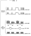
- optical packets with widely varying signal amplitudes can appear, closely spaced on the bus.
- this is shown by 203 where the packets PK1 (from a first transmitter) and PK2 (from a second transmitter) may have the same time slot width T1 and where packets PK1 have significantly higher signal amplitudes than the packets PK2.
- the circuit of FIG. 1 after a large amplitude packet PK1 threshold has been stored on C PD , then the circuit may not distinguish a small amplitude packet PK2 from noise. Therefore, such packets must be separated by a long enough time interval (e.g., T2 shown in 203) to allow C PD to discharge.
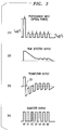
- the problem is illustrated in FIG. 3.
- the photocurrents I in(1) and I in(2) are proportional to the received optical signal powers P1 and P2 , and I in(1) is much larger than I in(2) .
- the peak detector output is determined by the first large I in(1) signal (pulse 0), and is too large for the peak of the first following I in(2) pulse (pulse 1) to reach the logic slicing level 331, of the quantizer circuit Q1 .
- the quantizer circuit Q1 output bit 1 is completely missing, (shown as dotted pattern) and bit 2 suffers a large pulse width distortion (in this example).
- a second problem in optical bus applications is the low frequency "dark level" optical power.
- FIG. 4 we illustratively depict the operating levels of a laser diode. It is impractical to modulate a transmitter's laser diode between its "true" OFF (i.e., P O , I O ) and its ON (i.e., P on , I on ) states at high speed. Consequently, lasers are typically biased OFF at a current I off (slightly below the lasing threshold current ( I th )) where there is some light output ( P OFF ) even in the OFF state. Extinction ratios ( P on / P off ) of 10 - 20 are typical.
- the dark (all off) light level could be NP off , where N is the number of lasers.
- This light-level approaches the ON-state light-level of an individual laser.
- the optical power of the dark level signal could exceed the burst signal level of some packets by a significant factor.
- logic threshold is I in Z T /2 , where I in is the input signal corresponding to the maximum optical signal input P in .
- I in is the input signal corresponding to the maximum optical signal input P in .
- a "false" logic threshold TH1 equal to (I dark + I in )Z T /2 is established rather than the "true” logic threshold TH2 equal to I in Z T/2 .
- I dark ⁇ I in as shown by 501
- proper input signal detection is still probable, as shown by 503.
- the false threshold TH1 would cause the input signal to be improperly detected, as shown by 504, rather than being properly detected, as shown by 505.
- FIG. 6 A simplified functional diagram of our new circuit is shown in FIG. 6.
- the preamp corresponding to A1 in FIG. 1, is a differential input/output transimpedance amplifier.
- the Adaptive Threshold Circuit 610 is a modified, enhanced version of the peak detector ( A2 , B X , B Y , C PD ) in FIG. 1.
- the Output Amplifier corresponds to A3
- the Packet Threshold Reset Circuitry (hereinafter Reset circuit) 620 is a new function, added to allow zeroing of the peak detector capacitor between data packets.
- the new capabilities are described in the following sections.
- the Reset function is introduced to each peak detector circuit and allows rapid and precise zeroing of the peak detector capacitor.
- the receiver By activating the Reset circuit 620 at the conclusion of a data packet (T2 of FIG. 2), the receiver is prepared to establish a new logic threshold (e.g., at a substantially reduced level) after a short reset interval.
- the dark level light problem is handled by a "dark level compensator" (Darcom) circuit (includes preamp A1 and Adaptive Threshold Circuit 610) which measures and shunts or subtracts out the low frequency input signal ( I comp ) portion of I in .
- the peak detector circuits A 2P , A 2N ), as described later, are modified to increase stability and improve the accuracy of peak detector tracking.
- a block diagram of the dark level compensator (Darcom) circuit 600 is shown in FIG. 6.
- Darcom circuit 600 consists of the input amplifier A1 , a positive peak detector A 2P , a negative peak detector A 2N , a comparison amplifier, A4 , and a low pass filter LP1 .
- Detector A 2P samples the peak value of the positive output of amplifier A1 .
- Detector A 2N samples the peak value of the negative output of amplifier A1 . Because of the differential outputs, ( V0+ and V0 ⁇ ) of amplifier A1 , the positive and negative peak detectors, A 2P and A 2N , can be implemented as identical circuits, thus assuring matching of tracking accuracy, and improving overall precision.
- Detector A 2P is used with amplifier A1 to set a logic threshold equal to half the maximum input swing (e.g., TH2 of FIG. 5).
- the Darcom circuit 600 relies on the spectral characteristics of the peak detector circuits ( A 2P , A 2N ). In the higher frequency range, bounded on the lower end by the discharge time of the peak detector capacitors, the peak detectors ( A 2P , A 2N ) act as peak sampling circuits with unity gain. At low frequencies, however, the peak detector capacitors have enough time to discharge, and consequently A 2P and A 2N are simply unity gain amplifiers. While the outputs of A 2P and A 2N do track low frequency variations in the input current I in , the following, for simplicity, refers to these low frequency variations as the "dc" I dark current.
- a 2P and A 2N apply the peak values of the positive and negative outputs ( V0+ and V0 ⁇ ) of amplifier A1 as inputs to comparison amplifier A4 .
- these peak detector outputs ( V0+ and V0 ⁇ ) consist of the sum of a high frequency common signal peak and a low frequency difference signal (dark level offset).
- A4 together with low pass filter LP1 converts this into a "dc difference" signal, ( I comp ) which is subtracted from the input signal I in .
- a dc (or low frequency) feedback loop is established in Darcom circuit 600 that forces the dc (or low frequency) signals' differential output of A1 to zero, cancelling out the input dark current ( I dark ) along with any other dc offset signals (or low frequency offset signals).
- Such other dc offset signals may be derived from the outputs V0+ and V0 ⁇ of amplifier A1 or from peak detectors A 2P orA 2N .
- Low pass filter LP1 serves to stabilize the Darcom feedback loop, and also to average out fluctuations in the dark level signal.
- Darcom circuit 600 ignores high frequency inputs, while forcing the dc (or low frequency) output component to zero.
- Proper operation of Darcom circuit 600 depends on accurate tracking and matching of the two peak detectors A 2P and A 2N . If the positive peak detector A 2P is inaccurate, then an improper logic threshold may be established, and the peak detector outputs will not be symmetric. This is illustrated by the wave forms 702 in FIG. 7. This may manifest itself as an offset in the differential PreAmp A1 output voltage ( V 0 + - V 0 - ). Likewise, if the peak detectors A 2P and A 2N do not precisely match each other, then the mismatch will again appear as a PreAmp A1 output offset.
- the gain of peak detector circuit A 2P was increased slightly.
- the fractional tracking error ( V in - V0 )/ V in is 1/(1 + A ), where A is the open loop gain of the amplifier A2 , and V in and V0 are the input and output signals of the peak detector consisting of A2 , B X , B Y , and C PD .
- the error is reduced with increasing gain A , but it never goes to zero.
- this loop is identified as the path leading from the positive output of A1 through the peak detector and then back to the negative input of A1 .
- Stability requires that there be a single dominant pole in this feedback loop. This is normally designed to be set by the peak detector capacitor C PD in series with the emitter drive resistance of transistor B X . Unhappily, there are many other poles in this loop, including the amplifier poles of A1 and A2 , as well as the input poles of A1 . Moreover, the driving resistance of B X is very small, and consequently a large capacitor C PD is needed to establish a dominant pole. Stability of this loop can become marginal.
- the peak detector A 2P operates in one of two modes: (1) charging or (2) maintenance.
- charging mode the positive input to amplifier A2 is greater than the negative input, and the circuit responds by pumping charge into the peak detector capacitor C PD .
- the charging mode the circuit is "slew limited”. Equivalently, the loop gain is zero, and thus stability is not at issue.
- maintenance mode the positive and negative inputs to amplifier A2 are approximately equal, and the charge pump B X on average provides just enough current to balance the discharge current (base current of B Y ). In this mode, stability is an issue, and must be assured.
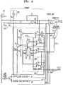
- Stability is improved by putting a large series resistance R PD in series with the charging transistor B X , as shown in FIG. 8. This lowers the frequency of the dominant pole, now determined approximately by R PD and C PD .
- the impaired charging characteristic that results is remedied by introducing a "slew booster" circuit 810, shown as amplifier A5 and charging transistor B Z in FIG. 8.
- the slew booster circuit 810 charges C PD directly, without a limiting series resistor.
- the input to amplifier A5 is offset slightly ( V OFF ) with respect to the input of A2 . Consequently, the slew booster turns on only when the difference between the input V 0 + and the stored output V OUT is large, i.e. > V OFF .
- the slew booster circuit 810 When the voltage stored on C PD charges to within V OFF of the final value, the slew booster circuit 810 turns off, and the main peak detector amplifier A2 charges C PD the rest of the way to equilibrium. Thus, the slew booster circuit 810 is "on" only when the circuit is in the charging mode. When the circuit is in the maintenance mode, the slew booster circuit 810 is off, and therefore does not affect overall feedback loop stability.
- the Reset circuit in response to an end-of-packet Reset signal, is designed to discharge both the positive and negative peak detector circuits A 2P and A 2N very rapidly so that data packets (PK1, PK2) differing in amplitude by approximately 100:1 (P1/P2) can be separated by a time interval (T2), illustratively, as short as four bit periods (this would be approximately 130ns for a 30Mb data signal).
- T2 shown in 203 of FIG. 2
- the Reset circuit includes a common Reset Enable Circuit 820 which generates a Reset enable signal from a reset signal and a Reset Discharge circuit 830 which is part of each peak detector circuit (830 is shown only for positive peak detector A 2P )
- the Reset circuit provides the following attributes: speed, precision, "clamp” function, power conservation and CMOS/TTL input levels.
- the first attribute, speed, is obtained by discharging or clamping the peak detector capacitor C PD as rapidly as possible. This requires, simply, a large discharge current ( I DIS ).
- the clamp function is necessary to turn the peak detector charging circuitry (i.e., amplifiers A2 and A5 ) off during the Reset interval, and likewise to turn-off the discharge circuitry (i.e., amplifier A6 ) during all but the Reset period.
- the clamp circuit also is used to force the packet receiver output (i.e., amplifiers A3 ) to a well-defined logic state during the Reset interval. Obviously, if amplifier A3 is part of quantizer circuit Q1 , then quantizer Q1 would be reset by the clamp function. Power conservation and CMOS/TTL input levels are system requirements.
- the Reset Discharge circuit 830 operates as follows. Comparator amplifier A6 compares the voltage across C PD with a precision reference voltage, V DIS . If it exceeds the reference voltage, V DIS then switch S F is closed and the discharge current I DIS is drawn from C PD .
- the precision reference V DIS is implemented as a two stage image circuit.
- the voltage V DIS essentially represents the initial output voltage V OUT when no input data is being received by the receiver of FIG. 8.
- the first stage, A 1i is a copy of input amplifier A1
- the second stage, A 2i is a copy of peak detector circuit A2 .
- the gain enhancing resistor, R1 used within the peak detector amplifier A2 , is referenced to the output 840 of the first image stage, A 1i ). Because I DIS is very large, in order to discharge capacitor C PD rapidly, the time delay through the amplifier A6 discharge loop must be short, or the capacitor C PD will be discharged too far. Likewise, the gain of amplifier A6 must be large to assure a precision discharge. Fortunately, stability is not a concern for the amplifier A6 loop because it can only discharge the capacitor, C PD not charge it; i.e. there is no restoring force to cause oscillation.
- the clamping function is effected by the Reset block 820 in FIG. 8.
- This circuit block translates the Reset input signal into the Reset enable clamping signals, and also turns on and off the discharge current, I DIS . This conserves power by minimizing power consumption of the Reset Discharge Circuit 830 at times when the Reset input signal is not present.
- a Reset discharge circuit may include a coarse discharge circuit 850 and a fine discharge circuit 830.
- the coarse discharge circuit 850 operates like the previous described discharge circuit 830 except that it is not activated unless the difference between voltage V OUT and V DIS exceeds the offset voltage V OFF1 .
- coarse discharge circuit 850 enables switch S C to connect current source I DIS2 to discharge capacitor C PD .
- the fine discharge circuit 830 is also activated since V OUT is greater than V DIS .
- the coarse discharge circuit 850 switches off the current source I DIS2 from capacitor C PD . Thereafter, only fine discharge circuit 830 is discharging capacitor C PD , ensuring a slower more accurately controllable discharge rate.
- the Reset discharge circuit Using the combined coarse and fine discharge circuits enables the Reset discharge circuit to 1) quickly discharge capacitor C PD of the peak voltage from a high power level packet data and 2) be able to very accurately discharge capacitor C PD down to the desired voltage V DIS .
- the coarse discharge circuit 850 may not be utilized at all. The end result is that the Reset discharge circuit enables the discharge rate to be increased (ensuring fast discharge) without sacrificing the accuracy of controlling the final discharge voltage.
- This arrangement allows the Reset circuit to discharge C PD rapidly and precisely without overshooting due to too great a discharge rate.
- the fast discharge rate ensures that the receiver can reset within a few bit times for a data rate which may vary from the tens to hundreds of megabits/s.
- the accuracy of setting the final discharge voltage of capacitor C PD ensures that the receiver's dynamic input signal range for adjacent packet data power levels can be about 100 to 1. That is, the receiver can detect a low level packet data signal which immediately follows a high level packet data signal which is 100 times as large as the low level signal.
- the dark level offset is determined by the difference between the output of A 2N and a new reference voltage which is analogous to the output of image circuit A 1i ; i.e., the amplifier A1 output with no dark level signal present.
- the comparison amplifier A4 would then remain a difference amplifier that would take the difference between the minimum peak voltages outputted from detector A 2N and this new reference.
- the difference amplifier together with a low pass filter would then produce the dc current I comp which is subtracted or shunted from I in prior to input to amplifier A1 .
- the receiver could be used with voltage input signals (rather than current input signals) by changing amplifier A1 from a transimpedance amplifier to a voltage amplifier. This is accomplished by replacing photodetector P D1 with a voltage signal source V S of specified output impedance. Such an arrangement would replace photodetector P D1 with the circuitry shown in the dotted blocks 860 and 870, where the voltage source V REF1 is a dc bias voltage and the voltage source V S is the input voltage signal.
- the resistors Z IN in 860 and 870 convert amplifier A1 from a transimpedance amplifier to a voltage amplifier.
- the analog circuit blocks are actually either well-known ECL gates, or simple modifications of ECL gates.
- the ECL gate consists of a differential pair with current source load, followed by an emitter follower stage. These circuits, while offering limited gain, are inherently very fast.
- the input amplifier, output amplifier, peak detectors A 2P and A 2N , amplifiers A5 and A6 , and precision references A 1i and A 2i may be implemented using circuits which are described in more detail in our previously referenced article.
- the circuit can be implemented using, for example, silicon, gallium arsenide or other appropriate semiconductor materials. Moreover, it is contemplated that other well-known circuits can be used to implement the amplifier circuit functions shown in FIG. 8 without departing from the teaching of the present invention.
- the present invention was described as a receiver for use in a burst mode operated packet data system, it could be utilized in a system that utilizes continuous data transmissions. Although the present invention has been described for use with optical signals, it should be understood that the present invention can be utilized in non-optical signals as well.
Landscapes
- Engineering & Computer Science (AREA)
- Computer Networks & Wireless Communication (AREA)
- Signal Processing (AREA)
- Physics & Mathematics (AREA)
- Electromagnetism (AREA)
- Power Engineering (AREA)
- Optical Communication System (AREA)
- Dc Digital Transmission (AREA)
- Transmission Systems Not Characterized By The Medium Used For Transmission (AREA)
- Circuits Of Receivers In General (AREA)
- Input Circuits Of Receivers And Coupling Of Receivers And Audio Equipment (AREA)
Applications Claiming Priority (2)
| Application Number | Priority Date | Filing Date | Title |
|---|---|---|---|
| US97603992A | 1992-11-13 | 1992-11-13 | |
| US976039 | 1992-11-13 |
Publications (1)
| Publication Number | Publication Date |
|---|---|
| EP0597633A1 true EP0597633A1 (fr) | 1994-05-18 |
Family
ID=25523655
Family Applications (1)
| Application Number | Title | Priority Date | Filing Date |
|---|---|---|---|
| EP93308838A Ceased EP0597633A1 (fr) | 1992-11-13 | 1993-11-04 | Récepteur numérique de données en mode rafales |
Country Status (4)
| Country | Link |
|---|---|
| US (1) | US5430766A (fr) |
| EP (1) | EP0597633A1 (fr) |
| JP (1) | JPH06232916A (fr) |
| CA (1) | CA2106439A1 (fr) |
Cited By (4)
| Publication number | Priority date | Publication date | Assignee | Title |
|---|---|---|---|---|
| EP0681378A1 (fr) * | 1994-05-02 | 1995-11-08 | AT&T Corp. | Récepteur de paquets de données avec sortie des données manipulée et effacement de l'éclairage de fond |
| EP0792012A2 (fr) * | 1996-02-23 | 1997-08-27 | Matsushita Electric Industrial Co., Ltd. | Amplificateur pour signaux de type burst et circuit récepteur optique |
| EP2073472A1 (fr) * | 2007-12-19 | 2009-06-24 | Eqcologic NV | Circuit de restauration de composant continu qui permet des données clairsemées |
| EP2834667A4 (fr) * | 2012-03-27 | 2015-11-04 | Pulsedlight Llc | Dispositif de mesure de distance optique |
Families Citing this family (45)
| Publication number | Priority date | Publication date | Assignee | Title |
|---|---|---|---|---|
| US5822104A (en) * | 1995-02-24 | 1998-10-13 | Nec Corporation | Digital optical receiving apparatus |
| JP3479154B2 (ja) * | 1995-04-04 | 2003-12-15 | 株式会社アドバンテスト | 信号弁別回路 |
| US5790295A (en) * | 1995-08-28 | 1998-08-04 | Apple Computer, Inc. | Gated integrator preamplifier for infrared data networks |
| US5801867A (en) * | 1996-03-20 | 1998-09-01 | Ericsson Raynet | DC-coupled receiver for shared optical system |
| US5828476A (en) * | 1996-06-11 | 1998-10-27 | The Boeing Company | Dual rate, burst mode, radiation hardened, optical transceiver |
| JP3758750B2 (ja) * | 1996-07-02 | 2006-03-22 | 富士通株式会社 | 光受信装置 |
| FI974225A (fi) * | 1997-11-13 | 1999-05-14 | Nokia Telecommunications Oy | Optinen vastaanotin |
| EP0981197A4 (fr) * | 1998-03-13 | 2005-03-30 | Matsushita Electric Ind Co Ltd | Circuit amplificateur, et recepteur optique equipe de ce circuit |
| JPH11317626A (ja) * | 1998-04-30 | 1999-11-16 | Sharp Corp | Fm復調器 |
| US6359941B1 (en) * | 1998-04-30 | 2002-03-19 | Lucent Technologies Inc. | System and method for improved reference threshold setting in a burst mode digital data receiver |
| JP3234573B2 (ja) * | 1998-08-31 | 2001-12-04 | 松下電器産業株式会社 | パケットフィルタリング装置 |
| US6785344B1 (en) | 2000-04-11 | 2004-08-31 | Terawave Communications, Inc. | Fast threshold determination for packet-multiplexed digital communication |
| US6735260B1 (en) * | 2000-04-17 | 2004-05-11 | Texas Instruments Incorporated | Adaptive data slicer |
| KR100381410B1 (ko) * | 2000-08-23 | 2003-04-23 | 학교법인 한국정보통신학원 | 다단 궤환형 버스트모드 광수신기 |
| US6420928B1 (en) | 2001-04-30 | 2002-07-16 | Quantum Bridge Communications, Inc. | AC coupled pre-amplifier for burst signal |
| US6963696B1 (en) * | 2001-04-30 | 2005-11-08 | Quantum Bridge Communications, Inc. | AC-coupled burst mode receiver with wide dynamic range |
| US7058315B2 (en) * | 2001-10-09 | 2006-06-06 | Chiaro Networks Ltd. | Fast decision threshold controller for burst-mode receiver |
| KR100630083B1 (ko) * | 2002-04-26 | 2006-09-27 | 삼성전자주식회사 | 버스트모드 광 수신기의 자동이득조절 장치 |
| US7729453B1 (en) * | 2002-04-26 | 2010-06-01 | Bing Li | System and method for fast dynamic adjustment of slicing level for burst mode optical receivers |
| US6774728B2 (en) * | 2002-12-20 | 2004-08-10 | Intel Corporation | Transimpedance amplifier |
| US6816010B2 (en) * | 2002-12-20 | 2004-11-09 | Intel Corporation | Transimpedance amplifier |
| US6833762B2 (en) * | 2002-12-20 | 2004-12-21 | Intel Corporation | Transimpedance ampifier |
| US6809596B2 (en) * | 2002-12-20 | 2004-10-26 | Intel Corporation | DC offset cancellation circuit, system and method |
| KR100547840B1 (ko) * | 2003-06-04 | 2006-01-31 | 삼성전자주식회사 | 빠른 세틀링 시간을 갖는 자동 이득 제어 장치 |
| KR100535311B1 (ko) * | 2003-12-18 | 2005-12-09 | 한국전자통신연구원 | 광 수신기의 문턱전압 제어 장치 |
| US7394996B2 (en) * | 2004-06-16 | 2008-07-01 | Industrial Technology Research Institute | Burst mode optical receiver and system and method therefor |
| CN100399727C (zh) * | 2004-08-27 | 2008-07-02 | 电子科技大学 | 一种光突发模式接收机 |
| DE102005002195A1 (de) * | 2005-01-17 | 2006-07-27 | Siemens Ag | Verfahren und Anordnung zur Regeneration eines optischen Datensignals |
| US7447395B2 (en) * | 2006-06-15 | 2008-11-04 | Sioptical, Inc. | Silicon modulator offset tuning arrangement |
| US7697793B2 (en) * | 2006-06-15 | 2010-04-13 | Lightwire, Inc. | Silicon modulator offset tuning arrangement |
| WO2008101758A1 (fr) * | 2007-02-21 | 2008-08-28 | Nokia Siemens Networks Gmbh & Co. Kg | Procédé de réception de signaux multiplex de salve optiques et récepteur en mode salve |
| JP5176505B2 (ja) * | 2007-12-03 | 2013-04-03 | 富士通オプティカルコンポーネンツ株式会社 | 光受信装置,光局側装置および光ネットワークシステム |
| US7525465B1 (en) * | 2008-02-19 | 2009-04-28 | Newport Media, Inc. | Reconfigurable and adaptive continuous time-sigma delta data converter |
| KR100972033B1 (ko) * | 2008-08-13 | 2010-07-23 | 한국전자통신연구원 | 전치 증폭기와 후치 증폭기가 단일로 집적된 기가비트 수동형 광 네트워크용 버스트 모드 수신기 |
| JP5280256B2 (ja) * | 2009-03-12 | 2013-09-04 | 住友電工デバイス・イノベーション株式会社 | 電子回路 |
| US20100254491A1 (en) * | 2009-04-01 | 2010-10-07 | General Electric Company | Dc offset compensating system and method |
| US8358940B2 (en) * | 2009-07-10 | 2013-01-22 | Luxtera Inc. | Method and system for optoelectronic receivers for uncoded data |
| KR101310904B1 (ko) * | 2009-11-30 | 2013-09-25 | 한국전자통신연구원 | 버스트 모드 수신기 및 타이밍 제어 방법 |
| JP2011142581A (ja) * | 2010-01-08 | 2011-07-21 | Fujitsu Optical Components Ltd | 光通信方法、光通信システム、光信号受信装置及び光信号送信装置 |
| US8705985B2 (en) | 2010-06-02 | 2014-04-22 | Mellanox Technologies Denmark Aps | Fast optical receiver for unencoded data |
| WO2013064158A1 (fr) | 2011-11-03 | 2013-05-10 | Iptronics A/S | Récepteur optique rapide |
| JP6107146B2 (ja) * | 2013-01-10 | 2017-04-05 | 富士通株式会社 | 光受信回路 |
| WO2017046067A1 (fr) | 2015-09-15 | 2017-03-23 | Firecomms Limited | Récepteur optique |
| WO2017046068A1 (fr) | 2015-09-15 | 2017-03-23 | Firecomms Limited | Récepteur optique comprenant une borne avant d'amplificateur cascode |
| US10819425B2 (en) * | 2018-07-09 | 2020-10-27 | Sumitomo Electric Industries, Ltd. | Transimpedance amplifier for receiving burst optical signal |
Citations (1)
| Publication number | Priority date | Publication date | Assignee | Title |
|---|---|---|---|---|
| EP0102174A2 (fr) * | 1982-07-26 | 1984-03-07 | Western Electric Company, Incorporated | Perfectionnements aux amplificateurs de transimpédance ou y relatifs |
Family Cites Families (19)
| Publication number | Priority date | Publication date | Assignee | Title |
|---|---|---|---|---|
| GB1603016A (en) * | 1978-05-31 | 1981-11-18 | Abbott Lab | Amplifier with dark current compensation |
| FR2473823A1 (fr) * | 1980-01-14 | 1981-07-17 | Dassault Electronique | Installation pour la transmission d'informations par ligne omnibus optique |
| CA1175919A (fr) * | 1980-02-20 | 1984-10-09 | Toshitaka Tsuda | Discriminateur de signaux avec correction du decalage continu |
| CA1212729A (fr) * | 1981-12-08 | 1986-10-14 | Hiroshi Ogawa | Circuit de detection et de correction de signaux numeriques avec generateur de signaux de portillonnage reglables |
| FR2579045B1 (fr) * | 1985-03-14 | 1988-03-04 | Bull Sa | Transducteur optoelectronique |
| JPS62132411A (ja) * | 1985-12-04 | 1987-06-15 | Hitachi Ltd | 利得・オフセツト制御回路 |
| US4736391A (en) * | 1986-07-22 | 1988-04-05 | General Electric Company | Threshold control with data receiver |
| US4781195A (en) * | 1987-12-02 | 1988-11-01 | The Boc Group, Inc. | Blood monitoring apparatus and methods with amplifier input dark current correction |
| US4926442A (en) * | 1988-06-17 | 1990-05-15 | International Business Machines Corporation | CMOS signal threshold detector |
| JPH0695741B2 (ja) * | 1988-07-27 | 1994-11-24 | 三菱電機株式会社 | 自動利得制御回路 |
| JPH0786513B2 (ja) * | 1988-12-14 | 1995-09-20 | 三菱電機株式会社 | データ受信装置 |
| US4905255A (en) * | 1989-01-03 | 1990-02-27 | American Telephone And Telegraph Company | Decision directed gain control |
| JPH0754335B2 (ja) * | 1989-01-31 | 1995-06-07 | 富士通株式会社 | ピーク値検出回路 |
| US5025456A (en) * | 1989-02-02 | 1991-06-18 | At&T Bell Laboratories | Burst mode digital data receiver |
| US4937842A (en) * | 1989-02-23 | 1990-06-26 | Motorola Inc. | Self adjusting data detector |
| US5119404A (en) * | 1990-08-06 | 1992-06-02 | Japan Aviation Electronics Industry Limited | Signal receiver |
| JP3021913B2 (ja) * | 1992-02-13 | 2000-03-15 | 日本電気株式会社 | 光受信装置 |
| JP2503837B2 (ja) * | 1992-07-16 | 1996-06-05 | 日本電気株式会社 | ディジタル光受信回路とディジタル光受信回路におけるプリアンプ回路 |
| JPH0810808B2 (ja) * | 1993-01-07 | 1996-01-31 | 日本電気株式会社 | 単極性符号・双極性符号変換回路 |
-
1993
- 1993-09-17 CA CA002106439A patent/CA2106439A1/fr not_active Abandoned
- 1993-11-04 EP EP93308838A patent/EP0597633A1/fr not_active Ceased
- 1993-11-12 JP JP5306080A patent/JPH06232916A/ja active Pending
-
1994
- 1994-08-22 US US08/293,908 patent/US5430766A/en not_active Expired - Lifetime
Patent Citations (1)
| Publication number | Priority date | Publication date | Assignee | Title |
|---|---|---|---|---|
| EP0102174A2 (fr) * | 1982-07-26 | 1984-03-07 | Western Electric Company, Incorporated | Perfectionnements aux amplificateurs de transimpédance ou y relatifs |
Non-Patent Citations (3)
| Title |
|---|
| AIKI ET AL: "446 Mbit/s integrated optical repeater", JOURNAL OF LIGHTWAVE TECHNOLOGY., vol. 3, no. 2, April 1985 (1985-04-01), NEW YORK US, pages 392 - 399, XP011422519, DOI: doi:10.1109/JLT.1985.1074201 * |
| BRACKETT ET AL: "A noise immune 32Mb/s optical data link", SIXTH EUROPEAN CONFERENCE ON OPTICAL COMMUNICATION, September 1980 (1980-09-01), YORK, GB, pages 458 - 461 * |
| OTA ET AL: "DC - 1 Gb/s burst-mode compatible receiver for optical bus applications", JOURNAL OF LIGHTWAVE TECHNOLOGY., vol. 10, no. 2, February 1992 (1992-02-01), NEW YORK US, pages 244 - 249, XP000267495, DOI: doi:10.1109/50.120581 * |
Cited By (7)
| Publication number | Priority date | Publication date | Assignee | Title |
|---|---|---|---|---|
| EP0681378A1 (fr) * | 1994-05-02 | 1995-11-08 | AT&T Corp. | Récepteur de paquets de données avec sortie des données manipulée et effacement de l'éclairage de fond |
| EP0792012A2 (fr) * | 1996-02-23 | 1997-08-27 | Matsushita Electric Industrial Co., Ltd. | Amplificateur pour signaux de type burst et circuit récepteur optique |
| EP0792012A3 (fr) * | 1996-02-23 | 1998-05-27 | Matsushita Electric Industrial Co., Ltd. | Amplificateur pour signaux de type burst et circuit récepteur optique |
| US5875049A (en) * | 1996-02-23 | 1999-02-23 | Matsushita Electric Industrial Co., Ltd. | Amplifier for burst signal and optical receiving circuit |
| EP2073472A1 (fr) * | 2007-12-19 | 2009-06-24 | Eqcologic NV | Circuit de restauration de composant continu qui permet des données clairsemées |
| EP2834667A4 (fr) * | 2012-03-27 | 2015-11-04 | Pulsedlight Llc | Dispositif de mesure de distance optique |
| US9581684B2 (en) | 2012-03-27 | 2017-02-28 | Garmin Switzerland Gmbh | Optical distance measurement device |
Also Published As
| Publication number | Publication date |
|---|---|
| JPH06232916A (ja) | 1994-08-19 |
| US5430766A (en) | 1995-07-04 |
| CA2106439A1 (fr) | 1994-05-14 |
Similar Documents
| Publication | Publication Date | Title |
|---|---|---|
| US5430766A (en) | Burst mode digital data receiver | |
| EP0597632B1 (fr) | Récepteur numérique pour données en mode paquet | |
| US4415803A (en) | Optical receiver with improved dynamic range | |
| EP0381371B1 (fr) | Récepteur numérique de données utilisant des rafales | |
| US6784750B2 (en) | Transimpedance amplifier with selective DC compensation | |
| US6909082B2 (en) | Automatic threshold control device for burst mode optical receiver | |
| KR100630089B1 (ko) | 차동 출력 구조의 버스트모드 광 수신기 | |
| US6118829A (en) | Apparatus and method for automatic mode selection in a communications receiver | |
| EP0611059B1 (fr) | Système pour récupérer une composante de courant continu pour les signaux binaires transférés en série | |
| KR100630083B1 (ko) | 버스트모드 광 수신기의 자동이득조절 장치 | |
| JPH06177664A (ja) | ディジタル光受信回路とトランスインピーダンスアンプ回路とプリアンプ回路 | |
| US9882539B1 (en) | Multi-data rate, burst-mode transimpedance amplifier (TIA) circuit | |
| US6191879B1 (en) | Offset control for burst-mode optical receiver | |
| KR100575981B1 (ko) | 버스트모드 광 수신기의 피크 및 바텀 검출기 | |
| US7330670B2 (en) | Bottom level detection device for burst mode optical receiver | |
| CN114389550A (zh) | 用于接收突发光信号的跨阻抗放大电路 | |
| US5111324A (en) | Optical receivers | |
| KR100381410B1 (ko) | 다단 궤환형 버스트모드 광수신기 | |
| Swartz et al. | A burst mode, packet receiver with precision reset and automatic dark level compensation for optical bus communications | |
| US5146476A (en) | High gain amplifier for reception of low level pulse code modulation nonreturn-to-zero signals | |
| US5561383A (en) | Switchable peak/average detect circuit | |
| Bauwelinck et al. | Current mode circuits for fast and accurate optical level monitoring with wide dynamic range | |
| JPS6370625A (ja) | 光受信回路 |
Legal Events
| Date | Code | Title | Description |
|---|---|---|---|
| PUAI | Public reference made under article 153(3) epc to a published international application that has entered the european phase |
Free format text: ORIGINAL CODE: 0009012 |
|
| AK | Designated contracting states |
Kind code of ref document: A1 Designated state(s): DE ES FR GB IT NL SE |
|
| RAP3 | Party data changed (applicant data changed or rights of an application transferred) |
Owner name: AT&T CORP. |
|
| 17P | Request for examination filed |
Effective date: 19941103 |
|
| 17Q | First examination report despatched |
Effective date: 19960605 |
|
| GRAG | Despatch of communication of intention to grant |
Free format text: ORIGINAL CODE: EPIDOS AGRA |
|
| STAA | Information on the status of an ep patent application or granted ep patent |
Free format text: STATUS: THE APPLICATION HAS BEEN REFUSED |
|
| 18R | Application refused |
Effective date: 19990313 |