EP0583014A1 - Datenmodulations- und Demodulationssystem für ein magnetisches Aufzeichnungssystem - Google Patents
Datenmodulations- und Demodulationssystem für ein magnetisches Aufzeichnungssystem Download PDFInfo
- Publication number
- EP0583014A1 EP0583014A1 EP93114259A EP93114259A EP0583014A1 EP 0583014 A1 EP0583014 A1 EP 0583014A1 EP 93114259 A EP93114259 A EP 93114259A EP 93114259 A EP93114259 A EP 93114259A EP 0583014 A1 EP0583014 A1 EP 0583014A1
- Authority
- EP
- European Patent Office
- Prior art keywords
- data
- clock pulse
- encoding
- frequency
- decoding
- Prior art date
- Legal status (The legal status is an assumption and is not a legal conclusion. Google has not performed a legal analysis and makes no representation as to the accuracy of the status listed.)
- Granted
Links
Images







Classifications
-
- G—PHYSICS
- G11—INFORMATION STORAGE
- G11B—INFORMATION STORAGE BASED ON RELATIVE MOVEMENT BETWEEN RECORD CARRIER AND TRANSDUCER
- G11B20/00—Signal processing not specific to the method of recording or reproducing; Circuits therefor
- G11B20/10—Digital recording or reproducing
-
- H—ELECTRICITY
- H03—ELECTRONIC CIRCUITRY
- H03M—CODING; DECODING; CODE CONVERSION IN GENERAL
- H03M5/00—Conversion of the form of the representation of individual digits
- H03M5/02—Conversion to or from representation by pulses
- H03M5/04—Conversion to or from representation by pulses the pulses having two levels
- H03M5/14—Code representation, e.g. transition, for a given bit cell depending on the information in one or more adjacent bit cells, e.g. delay modulation code, double density code
- H03M5/145—Conversion to or from block codes or representations thereof
-
- G—PHYSICS
- G11—INFORMATION STORAGE
- G11B—INFORMATION STORAGE BASED ON RELATIVE MOVEMENT BETWEEN RECORD CARRIER AND TRANSDUCER
- G11B20/00—Signal processing not specific to the method of recording or reproducing; Circuits therefor
- G11B20/10—Digital recording or reproducing
- G11B20/14—Digital recording or reproducing using self-clocking codes
- G11B20/1403—Digital recording or reproducing using self-clocking codes characterised by the use of two levels
- G11B20/1423—Code representation depending on subsequent bits, e.g. delay modulation, double density code, Miller code
- G11B20/1426—Code representation depending on subsequent bits, e.g. delay modulation, double density code, Miller code conversion to or from block codes or representations thereof
Definitions
- the present invention relates to a data modulation and demodulation system for use in a magnetic recording system. More particularly, it relates to a run length limited (RLL) type data modulation and demodulation system for a magnetic recording system.
- RLL run length limited
- write data is modulated under synchronization with a system clock signal and the modulated data is stored in a magnetic disc.
- the modulated and stored data is read and demodulated to restore original data used outside of the magnetic disc system.
- a data modulation and demodulation system is employed to achieve the above data encoding and decoding.
- variable length constant rate coding is carried out various ways, such as a coding of a (1,7) or 1/7 format with a rate of 2/3, hereinafter 1/7 coding, a coding of (2,7) or 2/7 format with a rate of 1/2, hereinafter 2/7 coding, and a coding of (1/8) or a 1/8 format.
- the 1/7 coding converts a data with a rate of 2/3: two bits to three bits, and inserts a zero ("0") bit(s), up to seven zero bits, between consecutive one (“1") bits data.
- the 2/7 coding converts a data with a rate of 1/2: one bit to two bits, and inserts at least two series zero ("0") bits, up to seven zero bits, between consecutive one (“1") bit data.
- the 1/7 coding does not require a high-speed operable circuit and has a wide data detection window, but has a disadvantage of a low recording density.
- the 2/7 coding achieves a high recording density, but requires a high-speed operation circuit.
- U.S. patent 4,488,142 discloses a (1,7) format encoding and decoding with a rate of 2/3. Embodiments of the present invention also use (1,7) format encoding and decoding with a rate of 2/3, i.e. 1/7 coding. However, U.S. patent 4,488,142 does not disclose a data modulation and demodulation system in which 1/7 coding is applied.
- a system for modulating and demodulating data written into and read from a magnetic recording medium in accordance with a run length limited method comprising:- a second clock pulse generating circuit arranged to receive a first clock pulse having a first frequency equal to a data write frequency, for generating a second clock pulse having a second frequency, said second frequency being two-thirds of said first frequency; and encoding means for encoding data to be written in accordance with a encoding, and decoding means for decoding other data to be read in accordance with a decoding, in response to said first and second clock pulses; characterised by:- a first clock pulse generating circuit receiving a reference signal and generating said first clock pulse in accordance with a phase of said reference signal, operatively connected to said second clock pulse generating circuit, wherein said first clock pulse generating circuit has:- switch means receiving a control signal and responsive thereto to switch a source of said reference signal between a reference clock and read data, for use in encoding and
- embodiments of the present invention can provide a data modulation and demodulation system to which a 1/7 coding is applied, and which is useful in a magnetic recording system.
- the system may be operable at low speed and can have a simple circuit construction.
- a first data modulation and demodulation system applied to a magnetic disc system will be described with a view to explaining the principles of the present invention.
- the data modulation and demodulation system includes a switch 8, a variable frequency oscillator (VFO) 1, a 1/3 frequency divider 2, a half (1/2) frequency divider 3, an AND gate 7, a bit register 4, a code register 5, and an encoding and decoding circuit 6. Since a data read is carried out under the 1/7 decoding, the bit register 4 has two bits. On the other hand, as a data write is carried out under the 1/7 encoding, the code register 5 has three bits. The encoding and decoding circuit 6 is used for the 1/7 encoding and the 1/7 decoding.
- the 1/3 frequency divider 2 and the 1/2 frequency divider 3 are used for a two bit to three bit conversion (encoding) when a data read operation is carried out, and a three bit to two bit conversion (decoding) when a data write operation is carried out.
- the switch 8 receives read data RD-DATA and a servo clock SERVO-CK and outputs the read data RD-DATA to the VFO 1 when the data read operation is carried out, or outputs the servo clock SERVO-CK when a data write operation is carried out.
- the VFO 1 receives the read data RD-DATA or the servo clock SERVO-CK as an input signal S IN and outputs a system clock CLK SYS having a stable frequency.
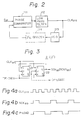
- the VFO 1 is realized by a phase-locked loop (PLL) circuit as shown in Fig. 2.
- the VFO 1 includes a phase comparator 111, a low pass filter 112, and a voltage controlled oscillator (VCO) 113.
- the VFO 1 also may include a 1/N frequency divider 114.
- the VFO 1 generates the system clock CLK SYS on the basis of the phase of the input signal S IN .
- FIG. 3 shows a circuit diagram of the 1/3 frequency divider 2.
- the 1/3 frequency divider 2 includes two J-K flip-flop (FF)s 21 and 22.
- the 1/3 frequency divider 2 outputs a bit data shift clock SCK BD , as shown in Fig. 4b, having a frequency that is one-third of the frequency of the system clock SLK SYS as shown in Fig. 4a.
- Figure 5 shows a circuit diagram of the 1/2 frequency divider 31.
- the 1/2 frequency divider 3 includes a D-FF 31.
- the 1/2 frequency divider 3 outputs a code data shift clock SCK CD having a frequency that is a half of that of the system clock SLK SYS .
- the AND gate 7 receives the bit data shift clock SCK BD from the 1/3 frequency divider 2 and the code data shift clock SCK CD from the 1/2 frequency divider 3 and outputs a parallel load signal P-LOAD as shown in Fig. 4c.
- Figure 6 shows a circuit diagram of an encoding and decoding unit 13 shown in Fig. 3 and consisting of the bit register 4, the code register 5, and the encoding and decoding circuit 6.
- the bit register 4 includes an NAND gate 41 receiving a read and write control signal R/W-CNT and the parallel load signal P-LOAD and outputting a mode signal S41 indicating a read mode or a write mode in response to the read and write control signal R/W-CNT.
- the read and write control signal R/W-CNT is a logical one: "1" when a read operation is carried out, but otherwise is a logical zero: "0".
- the bit register 4 also includes a BIT1 circuit having AND gates 42 and 43, an OR gate 44, and a D-FF 45, and a BIT0 circuit having AND gates 46 and 47, an OR gate 48, and a D-FF 49.
- the bit data shift clock SCK BD from the 1/3 frequency divider is supplied to clock terminals C of the D-FF's 45 and 49.
- a BIT WRITE DATA is supplied to a terminal of the AND gate 42 and to the D-FF 45 through the OR gate 44, and a positive (Q) output of the D-FF 45 is supplied to the AND gate 46 and to the D-FF 49.
- Decoded bit data which will be described later, can be supplied to the AND gates 43 and 47.
- Q outputs from the D-FF's 45 and 49 can also be supplied to the encoding and decoding circuit 6.
- bit register 4 Since the bit register 4 is used for both encoding and decoding, the decoded bit data is read when a data read operation is carried out, and the Q outputs are supplied when a data write operation is carried out.
- the bit register 4 operates in response to the parallel load signal P-LOAD from the AND gate.
- the code register 5 includes an inverter 51 and a NAND gate 52. These circuits correspond to the NAND gate 41 and function as a mode selector, except that a polarity of an output there from is an inversion of that of the NAND gate 41.
- the code register 5 also includes a CODE2 circuit having AND gates 53 and 54, an OR gate 55, and a D-FF 56, a CODE1 circuit having AND gates 57 and 58, an OR gate 59, and a D-FF 60, and a CODE0 circuit having AND gates 61 and 62, an OR gate 63, and a D-FF 64.
- the code data shift clock SCK CD from the 1/2 frequency divider 3 is supplied to clock terminals C of the D-FF's 56, 60, and 64.
- a CODE READ DATA is supplied to the D-FF's 56, 60, and 64 through the gates 53 and 55, the gates 57 and 59, and the gates 61 and 63, respectively.
- the code register 5 is also used for both encoding and decoding, and thus encoded bit data from the encoding and decoding circuit 6 can be supplied to the AND gates 54, 58 and 62, and Q outputs of the D-FF's 56, 60 and 64 also can be supplied to the encoding and decoding circuit 6.
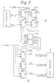
- Figure 7 shows a circuit diagram of the encoding and decoding circuit 6 when operated as a 1/7 encoder upon receipt of the read and write control signal R/W-CNT of "0", indicating a data write operation
- Figure 8 shows a circuit diagram of the encoding and decoding circuit 6 when operated as a 1/7 decoder.
- the encoding and decoding circuit 6 includes an encoding address generation circuit 61 having D-FF's 61a to 61d, a read-only-memory (ROM) 60a, and an encoded output circuit 62 having D-FF's 62a to 62c.
- the 1/7 coding is shown in Table 1 as an example. where X denotes a bit complementary to a preceding bit.
- Data is supplied from the bit register 4 as BIT0 and BIT1.
- Another 1/7 coding can be carried out as shown in the Table 2 disclosed in U.S.P. 4,488,142, and is known as an "Encoder State Dependent Table". where, * denotes "don't care", and 00 ⁇ means "not 00"
- the portion above the dotted line indicates the coding when the last bit Z3 of a previous coded data is zero ("0"), e.g. "100", and the portion below the dotted line indicates the coding when the last bit Z3 is one ("1"), e.g. "101".
- Symbols X1 to X4 and Z1 to Z3 in Fig. 7 correspond to those in Table 2.
- the ROM 60a stores a coding table as shown in Table 3. Note that Table 3 shows only a part of that coding table.
- the encoding and decoding circuit 6 includes a decoding address generation circuit 63 having D-FF's 63a to 63h, a ROM 60b, and a decoded output circuit 64 having D-FF's 64a and 64b.
- the encoding and decoding circuit 6 decodes data in accordance with the following Table 4, which is called a "Decoder State Dependent Table" in U.S.P.4,488,142. where, 00 ⁇ means "not 00", and X denotes "don't care”.
- ROM 60b stores a decoding table as shown in Table 5. Note, Table 5 shows only a part of that decoding table.
- the encoding and decoding circuit 6 is illustrated separately in Figs. 7 and 8. In practice, the encoding and decoding circuit 6 is combined with the circuits shown in Figs. 7 and 8.
- the ROMs 60a and 60b are formed by a single ROM.
- bi-directional busses are provided between the bit register 4 and the encoding and decoding circuit 6, and between the encoding and decoding circuit 6 and the code register 4. These busses are not shown in the Figures.
- the encoding circuit shown in Fig. 7 and the decoding circuit shown in Fig. 8 can be provided independently.
- the 1/2 frequency divider 3 provides the code data shift clock SCK CD used as a shift clock in the code register 5, i.e., a three bit shift register as shown in Fig. 6, and the 1/3 frequency divider 2 provides the bit data shift clock SCK BD used as a shift clock in the bit register 4, i.e., a two bit shift register as shown in Fig. 6.
- the code data shift clock SCK CD and the bit data shift clock SCK BD must be maintained in a fine synchronization state with a relationship of 2:3.
- the system clock CLK SYS must have a frequency f CLKSYS of the least common multiple of a frequency f SCKCD of the code data shift clock SCK CD and a frequency f SCKBD of the bit data shift clock SCK BD .
- f SCKCD is defined by a speed of the data write operation
- f SCKBD is defined by a speed of the data read operation.
- f SCKCD is 54 MHz and f SCKBD is 36 MHz
- the frequency f CLKSYS of the system clock CLK SYS is 108 MHz.
- the VFO 1 generates a system clock CLK SYS of 108 MHz.
- the switch 8 outputs the servo clock SERVO-CK to the VFO 1, to generate the system clock CLK SYS .
- the 1/3 frequency divider 2 outputs the bit data shift clock SCK BD
- the 1/2 frequency divider 3 outputs the code data shift clock SCK CD .
- the BIT WRITE DATA to be stored is supplied to the bit register 4 in synchronization with the system clock CLK SYS .
- the data input into the bit register 4 is shifted by the bit data shift clock SCK BD and stored in the D-FF's 45 and 49 shown in Fig. 6 as BIT1 and BIT0.
- This BIT1 and BIT0 data is loaded into the encoding and decoding circuit 6 in response to the parallel load signal P-LOAD from the AND gate 7, as shown in Fig. 4c.
- the loaded BIT1 and BIT0 are encoded (modulated) into three bit data in accordance with the 1/7 coding set forth above, and the encoded three bit data is read from the encoding and decoding circuit 6 to the code register 5 in response to the read and write control signal R/W-CNT, and stored in the D-FF's 56, 60 and 64 in the code register 5 as CODE2, CODE1 and CODE0, in response to the code data shift clock SCK CD .
- This three bit coded data is output as WRITE DATA to the magnetic disc.
- the output frequency of the WRITE DATA (or modulated data) from the code register 5 is 54 MHz.
- the switch 8 outputs the read data RD-DATA to the VFO 1, generating the system clock CLK SYS .
- CODE READ DATA which is read out in synchronization with the system clock CLK SYS , is supplied to the code register 5, and the data supplied to the code register 5 is stored in the D-FF's 56, 60 and 64 shown in Fig. 6 by the code data shift clock SCK CD from the 1/2 frequency divider 3.
- the CODE2 to CODE0 in the D-FF's 56, 60 and 64 are loaded into the encoding and decoding circuit 6 in response to the parallel load signal P-LOAD.
- the loaded three bit data is decoded (demodulated) into two bit data in accordance with the 1/7 decoding set forth above, and the decoded data is supplied to the bit register 4 in response to the read and write control signal R/W-CNT and stored in the D-FF's 45 and 49 in response to the bit data shift clock SCK BD from the 1/3 frequency divider 2.
- the output frequency of a READ DATA (or modulated data) from the bit register 4 is 36 MHz.
- the VFO 1 requires a source clock of 108 MHz when the read data frequency is 36 MHz and the write data frequency is 54 MHz.
- the realization of a VFO 1 operable over 100 MHz is difficult from the viewpoints of stability and cost.
- the data modulation and demodulation system includes the switch 8, a VFO 1', a 1/3 frequency divider 2', a two pulse generator 12, and the encoding and decoding unit 13 consisting of the bit register 4, the encoding and decoding circuit 6, and the code register 5.
- the switch 8 and the encoding and decoding unit 13 are substantially the same as those shown in Fig. 1.
- the circuit construction of the VFO 1', per se, is similar to that shown in Fig. 2, except that the VFO 1' operates at a lower frequency than that of the VFO 1 shown in Fig. 1.
- the 1/3 frequency divider 2' can be realized by the circuit shown in Fig. 3.
- a Q output of the J-K FF 22 of the 1/3 frequency divider is called a bit data shift gate clock SCKG BD
- a Q ⁇ output of the J-K FF 21 provides the parallel load signal P-LOAD as shown in Fig. 3 and Fig. 4C.
- the two pulse generator 12 is provided instead of the 1/2 frequency divider 3 shown in Fig. 1.
- the two pulse generator 12 generates two train pulses used for the bit data shift clock SCK BD on the basis of a bit data shift gate clock SCKG BD from the 1/3 frequency divider 2' and the system clock CLK SYS from the VFO 1'.
- Fig. 10 One version of the two pulse generator 12 used in the system of Fig. 9, is shown in Fig. 10.
- the two pulse generator 12 is an OR gate 121.
- the timing of the generation of the bit data shift clock SCK BD is shown in Figs. 11a to 11c.
- the bit data shift clock SCK BD has a frequency which is two-thirds that of a frequency of the system clock CLK SYS . Particular note should be taken of this frequency relationship.
- the system clock CLK SYS also can be used for the code data shift clock SCK CD supplied to the code register 5.
- the bit data shift clock SCK BD from the two pulse generator 12 is supplied to the bit register 4. Under the same conditions as those of the Fig.
- the VFO 1' is operable at a frequency of 54 MHz, which is a half of that of the VFO 1 shown in Fig. 1.
- bit data shift clock SCK BD shown in Fig. 11C is not evenly distributed, but is synchronized with the code data shift clock SCK CD : the system clock CLS SYS at a start of every bit data shift clock SCK BD as marked by small circles in Figs. 11a to 11c. This satisfies the requirement of the synchronization therebetween.
- FIG. 12a to 12j correspond to Figs. 11a to 11c
- Figures 12f and 12g show the two bit data BIT1 and BIT0 of the bit register 4
- Figures 12h to 12j show the three bit data CODE2 to CODE0 of the code register 5.
- the VFO 1' receives the servo clock SERVO-CK from the switch 8 and generates the system clock CLK SYS : the code data shift clock SCK CD of 54 MHz (Fig. 12a).
- the 1/3 frequency divider 2' outputs the parallel load signal P-LOAD (Fig. 12d), and the two pulse generator 12 outputs the bit data shift clock SCK BD of 36 MHz (Fig. 12c) to the bit register 4.
- the BIT WRITE DATA supplied to the bit register 4 is shifted by the bit data shift clock SCK BD and stored in the D-FF's 45 and 49 shown in Fig. 6 (Figs. 12e to 12g).
- the data BIT1 and BIT0 is loaded into the encoding and decoding circuit 6 in response to the parallel load signal P-LOAD, and the encoding and decoding circuit 6 carries out the two bits to three bits encoding in response to the read and write control signal which indicates the data write, and outputs the encoded data to the code register 5.
- the encoded data is stored in the code register 5 in response to a next parallel load signal P-LOAD and stored in the D-FF's 56, 60, and 64 shown in Fig. 6 by the code data shift clock SCK CD .
- the stored data CODE2 to CODE0 is output as code write (modulated) data.
- FIGS 13a to 13j are timing charts representing the data read operation.
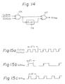
- FIG. 14 Another version of the two pulse generator 12 used in the system of Fig. 9 is shown in Fig. 14.
- the two pulse generator includes an AND gate 125, a delay circuit 126, and an OR gate 127.
- Figures 15a to 15c are timing charts representing the bit data shift clock SCK BD .
- the delay circuit 126 delays an output signal from the AND gate 126 by a time ⁇ T between times ⁇ T1 and ⁇ T2.
- the bit data shift clock SCK BD of Fig. 14 is evenly distributed.
- Figures 16a to 16j are timing charts representing the data write operation of the data modulation and demodulation system in which the circuit shown in Fig. 14 is applied.
- the operational principle of the data write is similar to that described above with reference to Figs. 12a to 12j.
- Figures 17a to 17j are timing charts illustrating the data read operation and correspond to Figs. 13a to 13j.
Landscapes
- Engineering & Computer Science (AREA)
- Signal Processing (AREA)
- Theoretical Computer Science (AREA)
- Signal Processing For Digital Recording And Reproducing (AREA)
Applications Claiming Priority (3)
| Application Number | Priority Date | Filing Date | Title |
|---|---|---|---|
| JP61292205A JPH061608B2 (ja) | 1986-12-08 | 1986-12-08 | デ−タの変復調装置 |
| JP292205/86 | 1986-12-08 | ||
| EP92122077A EP0536816B1 (de) | 1986-12-08 | 1987-12-08 | Datenmodulations- und Demodulationssystem für ein magnetisches Aufzeichnungssystem |
Related Parent Applications (1)
| Application Number | Title | Priority Date | Filing Date |
|---|---|---|---|
| EP92122077.8 Division | 1987-12-08 |
Publications (2)
| Publication Number | Publication Date |
|---|---|
| EP0583014A1 true EP0583014A1 (de) | 1994-02-16 |
| EP0583014B1 EP0583014B1 (de) | 1996-09-04 |
Family
ID=17778886
Family Applications (3)
| Application Number | Title | Priority Date | Filing Date |
|---|---|---|---|
| EP87310779A Expired - Lifetime EP0271317B1 (de) | 1986-12-08 | 1987-12-08 | Datenmodulations- und Demodulationssystem für ein magnetisches Aufzeichnungssystem |
| EP92122077A Expired - Lifetime EP0536816B1 (de) | 1986-12-08 | 1987-12-08 | Datenmodulations- und Demodulationssystem für ein magnetisches Aufzeichnungssystem |
| EP93114259A Expired - Lifetime EP0583014B1 (de) | 1986-12-08 | 1987-12-08 | Datenmodulations- und Demodulationssystem für ein magnetisches Aufzeichnungssystem |
Family Applications Before (2)
| Application Number | Title | Priority Date | Filing Date |
|---|---|---|---|
| EP87310779A Expired - Lifetime EP0271317B1 (de) | 1986-12-08 | 1987-12-08 | Datenmodulations- und Demodulationssystem für ein magnetisches Aufzeichnungssystem |
| EP92122077A Expired - Lifetime EP0536816B1 (de) | 1986-12-08 | 1987-12-08 | Datenmodulations- und Demodulationssystem für ein magnetisches Aufzeichnungssystem |
Country Status (5)
| Country | Link |
|---|---|
| US (1) | US4866544A (de) |
| EP (3) | EP0271317B1 (de) |
| JP (1) | JPH061608B2 (de) |
| KR (1) | KR910002746B1 (de) |
| DE (3) | DE3751898T2 (de) |
Families Citing this family (19)
| Publication number | Priority date | Publication date | Assignee | Title |
|---|---|---|---|---|
| US4823209A (en) * | 1987-11-05 | 1989-04-18 | Magnetic Peripherals Inc. | 1,7,2,3 Encoding/decoding employing 3/2 frequency division |
| JPH01286626A (ja) * | 1988-01-18 | 1989-11-17 | Hitachi Ltd | データ符号化方式 |
| CA2016957A1 (en) * | 1989-06-28 | 1990-12-28 | Lih-Jyh Weng | Data encoding and demodulation system |
| US5184125A (en) * | 1989-06-28 | 1993-02-02 | Digital Equipment Corporation | Data encoding and demodulation system |
| US5270714A (en) * | 1989-09-08 | 1993-12-14 | Fujitsu Limited | Encoding and decoding circuit for run-length-limited coding |
| US4964107A (en) * | 1990-03-14 | 1990-10-16 | International Business Machines Corporation | Relative timing precompensation of high-speed pulse signals for digital magnetic recoding |
| US6906700B1 (en) | 1992-03-05 | 2005-06-14 | Anascape | 3D controller with vibration |
| US6222525B1 (en) | 1992-03-05 | 2001-04-24 | Brad A. Armstrong | Image controllers with sheet connected sensors |
| JPH0828965B2 (ja) * | 1992-09-02 | 1996-03-21 | 日本電気株式会社 | 電圧変換回路 |
| US5424881A (en) | 1993-02-01 | 1995-06-13 | Cirrus Logic, Inc. | Synchronous read channel |
| JP3193810B2 (ja) * | 1993-08-31 | 2001-07-30 | 富士通株式会社 | 不揮発性半導体記憶装置及びその試験方法 |
| DE69327053T2 (de) * | 1993-09-21 | 2000-02-24 | Stmicroelectronics S.R.L., Agrate Brianza | Hochfrequenz Dekodierer mit Pipeline-Struktur für lauflängenbegrenzte Daten |
| DE69330957T2 (de) * | 1993-11-10 | 2002-04-04 | Stmicroelectronics S.R.L., Agrate Brianza | Programmierbarer RLL/NRZ-Dekoder für Einzel-/Doppel-Ausgangsdatenströme |
| US8674932B2 (en) | 1996-07-05 | 2014-03-18 | Anascape, Ltd. | Image controller |
| KR100370223B1 (ko) * | 2001-02-05 | 2003-02-05 | 삼성전자 주식회사 | 데이터 기록/재생 장치 및 그 방법과 데이터 부호화 방법 |
| JP4723756B2 (ja) * | 2001-06-06 | 2011-07-13 | 日本クラウンコルク株式会社 | 容器蓋 |
| US7526666B1 (en) * | 2006-09-06 | 2009-04-28 | Nvidia Corporation | Derived clock synchronization for reduced skew and jitter |
| US10298382B2 (en) * | 2016-06-23 | 2019-05-21 | Omnivision Technologies, Inc. | 1-16 and 1.5-7.5 frequency divider for clock synthesizer in digital systems |
| CN111405286B (zh) * | 2020-03-30 | 2023-11-03 | 沈阳航空产业技术研究院有限公司 | 一种自适应编解码双线信息传输方法和装置 |
Citations (4)
| Publication number | Priority date | Publication date | Assignee | Title |
|---|---|---|---|---|
| US3996613A (en) * | 1975-10-21 | 1976-12-07 | Sperry Rand Corporation | Data recording and transmission apparatus utilizing non-consecutive zero coding |
| US4005478A (en) * | 1974-09-16 | 1977-01-25 | Siemens Aktiengesellschaft | Process and arrangement for representing digital data by binary signals |
| EP0070387A2 (de) * | 1981-07-16 | 1983-01-26 | International Business Machines Corporation | Verfahren und Gerät zur Erzeugung von eines geräuschlos gleitenden Blockcodes für einen Kanal mit 2/3 Verhältnis |
| EP0090047A1 (de) * | 1981-09-25 | 1983-10-05 | Mitsubishi Denki Kabushiki Kaisha | System zur kodierung und entkodierung binärer daten |
Family Cites Families (6)
| Publication number | Priority date | Publication date | Assignee | Title |
|---|---|---|---|---|
| US4348640A (en) * | 1980-09-25 | 1982-09-07 | Rockwell International Corporation | Divide by three clock divider with symmertical output |
| US4488142A (en) * | 1981-12-31 | 1984-12-11 | International Business Machines Corporation | Apparatus for encoding unconstrained data onto a (1,7) format with rate 2/3 |
| US4503420A (en) * | 1982-05-07 | 1985-03-05 | Digital Equipment Corporation | Arrangement for encoding and decoding information signals |
| JPH07118657B2 (ja) * | 1985-04-15 | 1995-12-18 | 三菱電機株式会社 | 2進デ−タ符号化及び復号化方式 |
| US4688016A (en) * | 1985-06-13 | 1987-08-18 | International Business Machines Corporation | Byte-wide encoder and decoder system for RLL (1,7) code |
| US4675652A (en) * | 1986-04-11 | 1987-06-23 | Quantum Corporation | Integrated encoder decoder for variable length, zero run length limited codes |
-
1986
- 1986-12-08 JP JP61292205A patent/JPH061608B2/ja not_active Expired - Fee Related
-
1987
- 1987-12-07 KR KR8713911A patent/KR910002746B1/ko not_active Expired
- 1987-12-08 US US07/130,799 patent/US4866544A/en not_active Expired - Lifetime
- 1987-12-08 DE DE3751898T patent/DE3751898T2/de not_active Expired - Fee Related
- 1987-12-08 EP EP87310779A patent/EP0271317B1/de not_active Expired - Lifetime
- 1987-12-08 DE DE3789050T patent/DE3789050T2/de not_active Expired - Fee Related
- 1987-12-08 EP EP92122077A patent/EP0536816B1/de not_active Expired - Lifetime
- 1987-12-08 EP EP93114259A patent/EP0583014B1/de not_active Expired - Lifetime
- 1987-12-08 DE DE3789815T patent/DE3789815T2/de not_active Expired - Fee Related
Patent Citations (4)
| Publication number | Priority date | Publication date | Assignee | Title |
|---|---|---|---|---|
| US4005478A (en) * | 1974-09-16 | 1977-01-25 | Siemens Aktiengesellschaft | Process and arrangement for representing digital data by binary signals |
| US3996613A (en) * | 1975-10-21 | 1976-12-07 | Sperry Rand Corporation | Data recording and transmission apparatus utilizing non-consecutive zero coding |
| EP0070387A2 (de) * | 1981-07-16 | 1983-01-26 | International Business Machines Corporation | Verfahren und Gerät zur Erzeugung von eines geräuschlos gleitenden Blockcodes für einen Kanal mit 2/3 Verhältnis |
| EP0090047A1 (de) * | 1981-09-25 | 1983-10-05 | Mitsubishi Denki Kabushiki Kaisha | System zur kodierung und entkodierung binärer daten |
Also Published As
| Publication number | Publication date |
|---|---|
| JPH061608B2 (ja) | 1994-01-05 |
| DE3789050D1 (de) | 1994-03-24 |
| US4866544A (en) | 1989-09-12 |
| KR880008294A (ko) | 1988-08-30 |
| EP0536816B1 (de) | 1994-05-11 |
| JPS63144465A (ja) | 1988-06-16 |
| DE3751898D1 (de) | 1996-10-10 |
| DE3789815T2 (de) | 1994-08-18 |
| EP0271317B1 (de) | 1994-02-09 |
| EP0536816A1 (de) | 1993-04-14 |
| KR910002746B1 (en) | 1991-05-03 |
| EP0271317A3 (en) | 1989-11-15 |
| DE3789050T2 (de) | 1994-06-01 |
| EP0583014B1 (de) | 1996-09-04 |
| DE3751898T2 (de) | 1997-01-23 |
| EP0271317A2 (de) | 1988-06-15 |
| DE3789815D1 (de) | 1994-06-16 |
Similar Documents
| Publication | Publication Date | Title |
|---|---|---|
| EP0536816B1 (de) | Datenmodulations- und Demodulationssystem für ein magnetisches Aufzeichnungssystem | |
| EP1918929A1 (de) | Frequenz- und Phasensteuerungsvorrichtung sowie Decoder für maximale Wahrscheinlichkeit | |
| JPH06195893A (ja) | データ記録方法及び装置 | |
| JPH0683271B2 (ja) | 情報変換方式 | |
| KR930005644B1 (ko) | 제로 비복귀 반전방식(nrzi)의 변조신호 변환방법 및 그 장치 | |
| JP3417704B2 (ja) | ディジタル信号再生装置 | |
| US4831338A (en) | Synchronizing clock signal generator | |
| US3827078A (en) | Digital data retrieval system with dynamic window skew | |
| EP0090047B1 (de) | System zur kodierung und entkodierung binärer daten | |
| EP0210529A2 (de) | Schnittstellenschaltung für ein Floppydisk-Laufwerk | |
| US5598392A (en) | Data reproduction system synchronized by recording data | |
| KR950013833B1 (ko) | 동기데이타 도입방법 및 시스템 | |
| EP0315295A1 (de) | Gerät zum Kodieren und Dekodieren von Daten und ein Frequenzteiler im Verhältnis 3/2 | |
| CA1210515A (en) | Method of encoding a stream of data bits, device for carrying out the method, and device for decoding a stream of data bits | |
| WO1984004622A1 (fr) | Dispositif de reproduction de signaux numeriques | |
| EP0023783A1 (de) | Schaltungsanordnung zur Wiedergewinnung von Daten | |
| JPS62274948A (ja) | フレーム同期装置 | |
| KR860002165Y1 (ko) | Mfm 디지탈 변조 회로 | |
| KR0123760B1 (ko) | 바이페이즈 복조장치 | |
| KR100186394B1 (ko) | 광디스크 시스템의 비트클럭 회복장치 | |
| JP3010643B2 (ja) | 1―7rll変調方式エンコーダ回路 | |
| JP2673068B2 (ja) | レート2/5(2、18、2)符号を使用する2進データの符号化および復号の方法及び装置 | |
| KR100208377B1 (ko) | 디지탈 비디오 디스크 재생장치의 채널비트클럭 재생회로 | |
| KR910007655B1 (ko) | 디코딩회로 | |
| JPS6134306B2 (de) |
Legal Events
| Date | Code | Title | Description |
|---|---|---|---|
| PUAI | Public reference made under article 153(3) epc to a published international application that has entered the european phase |
Free format text: ORIGINAL CODE: 0009012 |
|
| 17P | Request for examination filed |
Effective date: 19930930 |
|
| AC | Divisional application: reference to earlier application |
Ref document number: 536816 Country of ref document: EP |
|
| AK | Designated contracting states |
Kind code of ref document: A1 Designated state(s): DE FR GB NL |
|
| 17Q | First examination report despatched |
Effective date: 19940516 |
|
| GRAH | Despatch of communication of intention to grant a patent |
Free format text: ORIGINAL CODE: EPIDOS IGRA |
|
| RBV | Designated contracting states (corrected) |
Designated state(s): DE FR GB |
|
| GRAH | Despatch of communication of intention to grant a patent |
Free format text: ORIGINAL CODE: EPIDOS IGRA |
|
| GRAA | (expected) grant |
Free format text: ORIGINAL CODE: 0009210 |
|
| AC | Divisional application: reference to earlier application |
Ref document number: 536816 Country of ref document: EP |
|
| AK | Designated contracting states |
Kind code of ref document: B1 Designated state(s): DE FR GB |
|
| REF | Corresponds to: |
Ref document number: 3751898 Country of ref document: DE Date of ref document: 19961010 |
|
| ET | Fr: translation filed | ||
| PLBE | No opposition filed within time limit |
Free format text: ORIGINAL CODE: 0009261 |
|
| 26N | No opposition filed | ||
| REG | Reference to a national code |
Ref country code: GB Ref legal event code: IF02 |
|
| PGFP | Annual fee paid to national office [announced via postgrant information from national office to epo] |
Ref country code: GB Payment date: 20031203 Year of fee payment: 17 |
|
| PGFP | Annual fee paid to national office [announced via postgrant information from national office to epo] |
Ref country code: FR Payment date: 20031210 Year of fee payment: 17 |
|
| PGFP | Annual fee paid to national office [announced via postgrant information from national office to epo] |
Ref country code: DE Payment date: 20031218 Year of fee payment: 17 |
|
| PG25 | Lapsed in a contracting state [announced via postgrant information from national office to epo] |
Ref country code: GB Free format text: LAPSE BECAUSE OF NON-PAYMENT OF DUE FEES Effective date: 20041208 |
|
| PG25 | Lapsed in a contracting state [announced via postgrant information from national office to epo] |
Ref country code: DE Free format text: LAPSE BECAUSE OF NON-PAYMENT OF DUE FEES Effective date: 20050701 |
|
| GBPC | Gb: european patent ceased through non-payment of renewal fee |
Effective date: 20041208 |
|
| PG25 | Lapsed in a contracting state [announced via postgrant information from national office to epo] |
Ref country code: FR Free format text: LAPSE BECAUSE OF NON-PAYMENT OF DUE FEES Effective date: 20050831 |
|
| REG | Reference to a national code |
Ref country code: FR Ref legal event code: ST |