EP0577998B1 - Field effect transistor - Google Patents
Field effect transistor Download PDFInfo
- Publication number
- EP0577998B1 EP0577998B1 EP93109418A EP93109418A EP0577998B1 EP 0577998 B1 EP0577998 B1 EP 0577998B1 EP 93109418 A EP93109418 A EP 93109418A EP 93109418 A EP93109418 A EP 93109418A EP 0577998 B1 EP0577998 B1 EP 0577998B1
- Authority
- EP
- European Patent Office
- Prior art keywords
- effect transistor
- field effect
- common
- gates
- drain region
- Prior art date
- Legal status (The legal status is an assumption and is not a legal conclusion. Google has not performed a legal analysis and makes no representation as to the accuracy of the status listed.)
- Expired - Lifetime
Links
- 230000005669 field effect Effects 0.000 title claims description 12
- 230000005611 electricity Effects 0.000 description 3
- 238000011161 development Methods 0.000 description 2
- 230000018109 developmental process Effects 0.000 description 2
- 238000013528 artificial neural network Methods 0.000 description 1
- 239000004020 conductor Substances 0.000 description 1
- 239000003669 enzymatically hydrolysed carboxymethyl cellulose Substances 0.000 description 1
Images

Classifications
-
- H—ELECTRICITY
- H10—SEMICONDUCTOR DEVICES; ELECTRIC SOLID-STATE DEVICES NOT OTHERWISE PROVIDED FOR
- H10D—INORGANIC ELECTRIC SEMICONDUCTOR DEVICES
- H10D30/00—Field-effect transistors [FET]
- H10D30/60—Insulated-gate field-effect transistors [IGFET]
- H10D30/611—Insulated-gate field-effect transistors [IGFET] having multiple independently-addressable gate electrodes influencing the same channel
-
- H—ELECTRICITY
- H10—SEMICONDUCTOR DEVICES; ELECTRIC SOLID-STATE DEVICES NOT OTHERWISE PROVIDED FOR
- H10D—INORGANIC ELECTRIC SEMICONDUCTOR DEVICES
- H10D30/00—Field-effect transistors [FET]
- H10D30/60—Insulated-gate field-effect transistors [IGFET]
Definitions
- the present invention relates to a field effect transistor.
- the present invention as claimed in claim 1 is invented considering the state above and has an object to provide a field effect transistor realizing highly intensive functions in a LSI.
- a field effect transistor relating to the present invention has a plural number of gates, and it generates an output by totalizing characteristics of "gate voltage vs. drain current" of the gates.
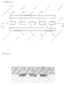
- Figure 1 shows a plane pattern in an embodiment of a field effect transistor relating to the present invention.
- Figure 2 shows vertical cross section of the embodiment.
- Figure 4 is a graph showing a characteristic of drain current of the field effect transistor of the embodiment.
- Figure 3 is a graph showing a characteristic of a drain current of a conventional field effect transistor.
- Figure 1 is a plane pattern of a field effect transistor of this invention, where a plural number of gates G1, G2....and Gn are set between source S and drain D. A conductor for impressing voltage to each gate is led upward, and the electricity is given from the upper positioned layer ( Figure 2). There is no interference of both of source S and drain D positioning in both sides of the gate, and the gate can be given electricity.
- a field effect transistor has an additional function in itself and realizes intensive functions and high density of functions to be equipped in a LSI.
- a field effect transistor relating to this invention establishes a plural number of gates and generates an output by totalizing of characteristics of "gate voltage vs. drain current" of the gates, so it has an effective result realizable a highly intensive function.
Landscapes
- Junction Field-Effect Transistors (AREA)
- Insulated Gate Type Field-Effect Transistor (AREA)
Applications Claiming Priority (2)
| Application Number | Priority Date | Filing Date | Title |
|---|---|---|---|
| JP179429/92 | 1992-06-12 | ||
| JP4179429A JPH0629520A (ja) | 1992-06-12 | 1992-06-12 | 電界効果トランジスタ |
Publications (3)
| Publication Number | Publication Date |
|---|---|
| EP0577998A2 EP0577998A2 (en) | 1994-01-12 |
| EP0577998A3 EP0577998A3 (esLanguage) | 1994-02-16 |
| EP0577998B1 true EP0577998B1 (en) | 1998-03-18 |
Family
ID=16065708
Family Applications (1)
| Application Number | Title | Priority Date | Filing Date |
|---|---|---|---|
| EP93109418A Expired - Lifetime EP0577998B1 (en) | 1992-06-12 | 1993-06-11 | Field effect transistor |
Country Status (4)
| Country | Link |
|---|---|
| EP (1) | EP0577998B1 (esLanguage) |
| JP (1) | JPH0629520A (esLanguage) |
| KR (1) | KR940001458A (esLanguage) |
| DE (1) | DE69317480T2 (esLanguage) |
Family Cites Families (4)
| Publication number | Priority date | Publication date | Assignee | Title |
|---|---|---|---|---|
| US3355598A (en) * | 1964-11-25 | 1967-11-28 | Rca Corp | Integrated logic arrays employing insulated-gate field-effect devices having a common source region and shared gates |
| JPS5753151A (en) * | 1980-09-16 | 1982-03-30 | Nippon Telegr & Teleph Corp <Ntt> | And circuit |
| JPH0695570B2 (ja) * | 1985-02-07 | 1994-11-24 | 三菱電機株式会社 | 半導体集積回路装置 |
| US5005059A (en) * | 1989-05-01 | 1991-04-02 | Motorola, Inc. | Digital-to-analog converting field effect device and circuitry |
-
1992
- 1992-06-12 JP JP4179429A patent/JPH0629520A/ja active Pending
-
1993
- 1993-06-02 KR KR1019930009886A patent/KR940001458A/ko not_active Withdrawn
- 1993-06-11 DE DE69317480T patent/DE69317480T2/de not_active Expired - Fee Related
- 1993-06-11 EP EP93109418A patent/EP0577998B1/en not_active Expired - Lifetime
Also Published As
| Publication number | Publication date |
|---|---|
| EP0577998A3 (esLanguage) | 1994-02-16 |
| DE69317480T2 (de) | 1998-07-09 |
| EP0577998A2 (en) | 1994-01-12 |
| KR940001458A (ko) | 1994-01-11 |
| DE69317480D1 (de) | 1998-04-23 |
| JPH0629520A (ja) | 1994-02-04 |
Similar Documents
| Publication | Publication Date | Title |
|---|---|---|
| JP2912174B2 (ja) | ライブラリ群及びそれを用いた半導体集積回路 | |
| JPS56116670A (en) | Semiconductor integrated circuit device and manufacture thereof | |
| JPS6124250A (ja) | 半導体集積回路装置 | |
| US7207025B2 (en) | Sea-of-cells array of transistors | |
| US5768146A (en) | Method of cell contouring to increase device density | |
| EP0577998B1 (en) | Field effect transistor | |
| EP0349255A3 (en) | A thin-film transistor array | |
| JPH04216668A (ja) | 半導体集積回路 | |
| JPS61193467A (ja) | 半導体集積回路装置 | |
| US5798541A (en) | Standard semiconductor cell with contoured cell boundary to increase device density | |
| JPS59167049A (ja) | 半導体装置 | |
| JPS58166743A (ja) | マスタ−スライス基板 | |
| JPS5895855A (ja) | 半導体集積回路装置の設計方法 | |
| KR20240112387A (ko) | Pim 구현을 위한 반도체 소자 | |
| KR0144243B1 (ko) | 게이트 어레이의 입출력 셀 레이아웃 방법 | |
| TW329052B (en) | Semiconductor device | |
| KR0167684B1 (ko) | 반도체 메모리 소자내의 기준전압 발생회로의 배치 방법 | |
| Karpovich et al. | In/out pad electrostatic discharge protection for sub-micron integrated circuits based on lateral bipolar transistor | |
| JPH09153286A (ja) | 半導体記憶装置 | |
| 장태진 | A Novel Design of Overpass Channel Synapse Array with Ultra-Low Power Operation for Neuromorphic Systems | |
| JPS60247943A (ja) | 半導体集積回路装置 | |
| JP2652948B2 (ja) | 半導体集積回路 | |
| JPH0237749A (ja) | マスタースライス型半導体装置 | |
| JPH01152642A (ja) | 半導体集積回路 | |
| JPH0475665B2 (esLanguage) |
Legal Events
| Date | Code | Title | Description |
|---|---|---|---|
| PUAI | Public reference made under article 153(3) epc to a published international application that has entered the european phase |
Free format text: ORIGINAL CODE: 0009012 |
|
| PUAL | Search report despatched |
Free format text: ORIGINAL CODE: 0009013 |
|
| AK | Designated contracting states |
Kind code of ref document: A2 Designated state(s): DE FR GB |
|
| AK | Designated contracting states |
Kind code of ref document: A3 Designated state(s): DE FR GB |
|
| 17P | Request for examination filed |
Effective date: 19940114 |
|
| 17Q | First examination report despatched |
Effective date: 19950104 |
|
| RAP1 | Party data changed (applicant data changed or rights of an application transferred) |
Owner name: SHARP KABUSHIKI KAISHA Owner name: YOZAN INC. |
|
| GRAG | Despatch of communication of intention to grant |
Free format text: ORIGINAL CODE: EPIDOS AGRA |
|
| GRAG | Despatch of communication of intention to grant |
Free format text: ORIGINAL CODE: EPIDOS AGRA |
|
| GRAH | Despatch of communication of intention to grant a patent |
Free format text: ORIGINAL CODE: EPIDOS IGRA |
|
| GRAH | Despatch of communication of intention to grant a patent |
Free format text: ORIGINAL CODE: EPIDOS IGRA |
|
| GRAA | (expected) grant |
Free format text: ORIGINAL CODE: 0009210 |
|
| AK | Designated contracting states |
Kind code of ref document: B1 Designated state(s): DE FR GB |
|
| REF | Corresponds to: |
Ref document number: 69317480 Country of ref document: DE Date of ref document: 19980423 |
|
| PG25 | Lapsed in a contracting state [announced via postgrant information from national office to epo] |
Ref country code: GB Free format text: LAPSE BECAUSE OF NON-PAYMENT OF DUE FEES Effective date: 19980618 |
|
| ET | Fr: translation filed | ||
| PLBE | No opposition filed within time limit |
Free format text: ORIGINAL CODE: 0009261 |
|
| STAA | Information on the status of an ep patent application or granted ep patent |
Free format text: STATUS: NO OPPOSITION FILED WITHIN TIME LIMIT |
|
| GBPC | Gb: european patent ceased through non-payment of renewal fee |
Effective date: 19980618 |
|
| PG25 | Lapsed in a contracting state [announced via postgrant information from national office to epo] |
Ref country code: FR Free format text: LAPSE BECAUSE OF NON-PAYMENT OF DUE FEES Effective date: 19990226 |
|
| 26N | No opposition filed | ||
| PG25 | Lapsed in a contracting state [announced via postgrant information from national office to epo] |
Ref country code: DE Free format text: LAPSE BECAUSE OF NON-PAYMENT OF DUE FEES Effective date: 19990401 |
|
| REG | Reference to a national code |
Ref country code: FR Ref legal event code: ST |