EP0575997A2 - Dispositif de traitement de signal d'un enregistreur à cassette vidéo numérique - Google Patents
Dispositif de traitement de signal d'un enregistreur à cassette vidéo numérique Download PDFInfo
- Publication number
- EP0575997A2 EP0575997A2 EP19930110060 EP93110060A EP0575997A2 EP 0575997 A2 EP0575997 A2 EP 0575997A2 EP 19930110060 EP19930110060 EP 19930110060 EP 93110060 A EP93110060 A EP 93110060A EP 0575997 A2 EP0575997 A2 EP 0575997A2
- Authority
- EP
- European Patent Office
- Prior art keywords
- sync
- sync blocks
- blocks
- block
- high frequency
- Prior art date
- Legal status (The legal status is an assumption and is not a legal conclusion. Google has not performed a legal analysis and makes no representation as to the accuracy of the status listed.)
- Granted
Links
Images

Classifications
-
- H—ELECTRICITY
- H04—ELECTRIC COMMUNICATION TECHNIQUE
- H04N—PICTORIAL COMMUNICATION, e.g. TELEVISION
- H04N5/00—Details of television systems
- H04N5/76—Television signal recording
- H04N5/91—Television signal processing therefor
- H04N5/93—Regeneration of the television signal or of selected parts thereof
- H04N5/94—Signal drop-out compensation
- H04N5/945—Signal drop-out compensation for signals recorded by pulse code modulation
-
- G—PHYSICS
- G11—INFORMATION STORAGE
- G11B—INFORMATION STORAGE BASED ON RELATIVE MOVEMENT BETWEEN RECORD CARRIER AND TRANSDUCER
- G11B20/00—Signal processing not specific to the method of recording or reproducing; Circuits therefor
- G11B20/10—Digital recording or reproducing
- G11B20/18—Error detection or correction; Testing, e.g. of drop-outs
-
- H—ELECTRICITY
- H04—ELECTRIC COMMUNICATION TECHNIQUE
- H04N—PICTORIAL COMMUNICATION, e.g. TELEVISION
- H04N19/00—Methods or arrangements for coding, decoding, compressing or decompressing digital video signals
- H04N19/85—Methods or arrangements for coding, decoding, compressing or decompressing digital video signals using pre-processing or post-processing specially adapted for video compression
- H04N19/89—Methods or arrangements for coding, decoding, compressing or decompressing digital video signals using pre-processing or post-processing specially adapted for video compression involving methods or arrangements for detection of transmission errors at the decoder
- H04N19/895—Methods or arrangements for coding, decoding, compressing or decompressing digital video signals using pre-processing or post-processing specially adapted for video compression involving methods or arrangements for detection of transmission errors at the decoder in combination with error concealment
-
- H—ELECTRICITY
- H04—ELECTRIC COMMUNICATION TECHNIQUE
- H04N—PICTORIAL COMMUNICATION, e.g. TELEVISION
- H04N5/00—Details of television systems
- H04N5/76—Television signal recording
- H04N5/91—Television signal processing therefor
- H04N5/92—Transformation of the television signal for recording, e.g. modulation, frequency changing; Inverse transformation for playback
- H04N5/926—Transformation of the television signal for recording, e.g. modulation, frequency changing; Inverse transformation for playback by pulse code modulation
- H04N5/9261—Transformation of the television signal for recording, e.g. modulation, frequency changing; Inverse transformation for playback by pulse code modulation involving data reduction
- H04N5/9264—Transformation of the television signal for recording, e.g. modulation, frequency changing; Inverse transformation for playback by pulse code modulation involving data reduction using transform coding
Definitions
- the present invention relates to a signal processing apparatus for concealing uncorrectable errors during signal reproduction in a digital signal recording and reproducing apparatus for digitizing a video signal and recording and reproducing the digitized signal.
- Digital VCRs which record and reproduce a digitized video signal to achieve significantly better image quality in consumer-class video devices, are widely expected to replace today's analog VCRs as the next generation in video components.
- One of the greatest advantages of the digital VCR is the nearly total absence of signal deterioration through multiple generations of dubbing and editing, and digital VCRs are already used in broadcasting and other commercial applications.
- To achieve a long playing time in a compact cassette requires the efficient reduction of the image data by means of bit rate reduction processing.
- the structure and operation of a digital VCR using bit rate reduction is described briefly below.
- the first step during recording is to convert the input video signal to a digital signal using an analog/digital (A/D) converter, after which the signal is compressed to a predetermined data quantity by a bit rate reduction encoder.
- the discrete cosine transformation (DCT) method is widely used for bit rate reduction or video signals because of the compression efficiency of the method.
- DCT discrete cosine transformation
- plural pixels are grouped into blocks, and the blocks are then converted to a frequency domain.
- the data can be efficiently compressed by variable length coding according to the converted coefficient.
- the encoding efficiency can be increased in this case by increasing the length of the variable length coding units. Doing so, however, also increases the range of error propagation when an error occurs.
- a coding method whereby variable length coding is applied with plural block units (“compression blocks” below) has been proposed in Japanese patent application number 1989-147891 for use in a digital VCR with a higher error probability than other transmission paths.
- Error correction parity is then added by the error correction encoder, and a synchronization signal and identification data (ID) are added to create recording blocks ("sync blocks" below).
- ID synchronization signal and identification data
- sync blocks include the synchronization signal "sync" for detecting the sync blocks from the reproduced signal, the track number for correctly writing the reproduced sync block to memory, the sync block number and/or other identification information (ID), the video signal in a bit rate reduction form, and error correction parity (inner parity) data. These sync blocks are then aligned with the track and recorded to tape.
- the sync blocks are detected from the signal reproduced by the playback head and demodulated, and error correction is applied by the error correction decoder based on the error correction parity added during recording. Any uncorrectable errors are then concealed in the bit rate reduced state by the error concealment processor.
- the error correction process can correct up to a certain number of errors. When the tape is scratched or otherwise damaged, resulting in significant signal dropout, however, the amount of errors exceeds the correction capability of the process, and error correction becomes impossible. When such uncorrectable errors occur, concealment is used so that the effect of the errors is not visually conspicuous. Because the effect of these errors is propagated through the completed range of variable length coding, concealment is achieved by the error concealment processor substituting a previous corresponding sync block for the complete sync block containing the compression block in which the error is found. The concealed data is then decoded to the original data by the bit rate reduction decoder, converted to an analog signal by the D/A converter, and output.
- an object of the present invention is to minimize visually discernible image deterioration in a digital VCR using bit rate reduction coding by means of error concealment, and to enable error concealment using a small-scale circuit by concealment in a bit rate reduction state.
- a signal processing apparatus for use in a digital video signal reproducing apparatus reproduces digital signal presented in sync blocks each having a LOW REGION area and HIGH REGION area and an N (N is a positive integer) number of subsequent sync blocks defining a sharing group for sharing HIGH REGION areas for storing high frequency data.
- the signal processing apparatus comprises, error correction means for correcting errors in said sync blocks; error flag providing means for providing an error flag to a sync block which still has an error remaining after the processing in said error correction means and for selecting an errorless sync block which has no error; memory means for storing errorless sync blocks of one frame; substitution means for passing said errorless sync block and for substituting a sync block stored in said memory means for a sync block having an error flag; holding means for holding said N number of sync blocks produced from said substitution means; substitution detection means for detecting a presence of at least one to (N-1) substitute sync block in said N sync blocks stored in said holding means; and HIGH REGION area trimming means for passing without any change said N sync blocks produced from said holding means when no substitute sync block is detected, but for trimming the HIGH REGION area from each of said N sync blocks produced from said holding means when one to (N-1) substitute sync block is detected by said substitution detection means.
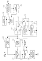
- Fig. 1 is a block diagram of a reproducing portion of a digital VCR, particularly showing a signal processing apparatus for a digital video signal reproducing apparatus according to the present invention.
- the bit rate reduction encoder comprises an input 200 for receiving an analog video signal, an A/D converter 201, a one frame memory 202 for storing digital video signal of one frame, a discrete cosine transformation (DCT) operator 203 for performing the discrete cosine transformation operation, a quantizer 204, a variable length coding encoder 205, a memory 206 for inserting the variable length coded data to sync blocks, an error correction coding encoder 207 for adding inner error correction codes, outer error correction codes and other necessary codes such as sync code and ID code, a recording processor 208 for presenting sync blocks ready to be recorded on a magnetic tape, and an output 209 for outputting the sync blocks to a recording head (not shown) for recording on a recording tape.
- DCT discrete cosine transformation
- the digital video signal from A/D converter 201 is written to the one frame memory 202 accommodating one frame of the digital video signal.
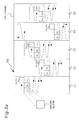
- One frame memory 202 is diagrammatically shown in Fig. 3a.
- memory 202 carrying n-th frame data is divided into five columns C1, C2, C3, C4 and C5. From a preselected point in each of five columns C1, C2, C3, C4 and C5, a block data covering 64 pixels (8 pixels X 8 lines) is extracted to provide five macro blocks 1n, 2n, 3n, 4n and 5n.
- the extraction is carried out such that from each macro block four brightness signal sub-blocks and two color difference signal sub-blocks (one R-Y sub-block and one B-Y sub-block) are read.
- Each compression that will be carried out DCT operation thus comprises thirty (30) sub-blocks.
- the input video signal is thus a 4:2:2 component signal, and the color difference signals are sampled every other line.
- each of the five extracted macro blocks 1n, 2n, 3n, 4n and 5n is then processed in DCT operator 203, quantizer 204, variable length coding encoder 205, memory 206 and error correction coding encoder 207 to present five sync blocks 1n, 2n, 3n, 4n and 5n.
- DCT operator 203 quantizer 204
- variable length coding encoder 205 variable length coding encoder 205
- memory 206 error correction coding encoder 207
- variable length coding encoder 205 In the DCT operator 203, quantizer 204, variable length coding encoder 205, memory 6 and error correction coding encoder 207, the following operations are carried out for five macro blocks, such as 1n-5n, to provide five sync blocks.
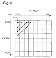
- the data from one block is converted by DCT operation to obtain frequency components analyzed in horizontal and vertical directions, and the DCT converted result will be plotted on 8x8 graph, as shown in Fig. 4, so that each box in 8x8 graph will carry amount of frequency component analyzed by the DCT operation.
- the DC component will be stored in box 400, and the AC components will be stored in other boxes, such that higher the frequency, further away from box 400 the storing box will be.
- DCT converted data will have only DC component.
- the DCT converted data will be given only in box 400, and all the remaining boxes will carry "0s".
- DCT converted data will have low frequency components in the vertical analyzed direction, but low and high frequency components in the horizontal analyzed direction.
- the DCT converted data will be plotted in the boxes of the upper first to several rows in the 8x8 graph, and the remaining boxes will carry "0s".
- DCT converted data will have low frequency components in the horizontal analyzed direction, but low and high frequency components in the vertical analyzed direction.
- the DCT converted data will be plotted in the boxes of the first to several columns from the left side in the 8x8 graph, and the remaining boxes will carry "0s".
- DCT converted data will have low and high frequency components in both vertical and horizontal directions.
- the DCT converted data will be plotted in almost all the boxes in the 8x8 graph.
- the reading starts from the DC component in box 400 and proceeds in a zigzag pattern from the low frequency component to high frequency component, as shown by an arrow in Fig. 4.
- the read data will be stored in memory 206.
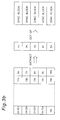
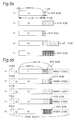
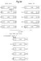
- Fig. 5a an example of read data for five macro blocks 1n, 2n, 3n, 4n and 5n is shown. Note that some data are longer than other data. However, quantization is controlled by quantizer 204 so that total length of five variable length coded data for five macro blocks is always a constant, such as 385 (77x5) bytes including information of quantization and other information, such as two reset flags (0,0) at the beginning of sync block.
- a predetermined amount of data such as 60 byte data, from the lowest frequency data is defined as a LOW FREQUENCY data, and the data exceeding the 60 byte data is defined as a HIGH FREQUENCY data.
- the data for five macro blocks 1n, 2n, 3n, 4n and 5n are rearranged such that the LOW FREQUENCY data 1L, 2L, 3L, 4L and 5L are maintained the same, but the HIGH FREQUENCY data are sequentially shifted, as shown in Fig. 5b, to make each macro block equal to 77 bytes. Therefore, some macro block may carry HIGH FREQUENCY data which belongs to other sync block. Also, all the HIGH FREQUENCY data for these five macro blocks can be found within the same five sync blocks. Thus, these five macro blocks are mutually sharing the HIGH FREQUENCY area for the HIGH FREQUENCY data, and are called five macro blocks of a sharing group.
- the five sync blocks which share the HIGH FREQUENCY area for the HIGH FREQUENCY data are called five sync blocks of a sharing group.
- the sync blocks are sequentially outputted through the output 209, so that the sync blocks are sequentially recorded on a recording tape.
- the signal processing apparatus comprises an input 100 for receiving sync blocks from magnetic tape, a reproducing processor 102 for separately producing each sync block, an inner correction decoder 104 for effecting an inner correction such as by inner parity by the inner code added in the error correction coding encoder 207, a memory 108 for storing one frame data consisting of plural sync blocks and also for storing error flags for respective sync blocks, as shown in Fig. 6, and an outer correction decoder 106 for effecting an outer correction such as by outer parity.
- memory 108 stores the sync blocks in parallel to each other and some errors found in the sync blocks are corrected by inner codes and outer codes. However, if the errors are more than that can be corrected by the inner and outer codes, an error flag is set to "1" to the sync block which still has some errors. The sync block with no error has an error flag reset to "0".
- switches 110 and 112 are switched to terminal C.
- the error sync block along line L1 diminishes at the terminal T, and in turn, the substitution memory 114 reads a substitute sync block of one previous frame from an area which should be supplied with the new sync block.
- the substitute sync block is transmitted along line L4 to a concealment flag setting circuit 116 for setting a concealment flag at the first bit of the two front bits in the substitute sync block.
- the substitute sync block is transmitted along line L5 and switch 110 back to substitution memory 114 for overwriting the substitute sync block with the concealment flag being set and, at the same time, along line L6 and switch 112 to delay 118.
- switches 110 and 112 are changed to terminal C during a moment for sending the second sync block 2n.
- the second sync block 2n is replaced with a substitute sync block 2(n-1) from the previous frame as stored in substitution memory.
- the concealment flag for the second sync block 2(n-1) is set to "1".
- the sync blocks from switch 112 are provided to the delay 118.
- the delay 118 holds the data until five sync blocks of one sharing group are stored.
- they are sequentially transmitted to a HIGH FREQUENCY TRIM flag setting circuit 122. Then, the delay 118 is reset, ready for receiving next five sync blocks of another sharing group.
- the sync blocks from switch 112 are also applied to a concealment flag detector 120 which detects only the concealment flag bit, i.e., the first bit, of the sync blocks.
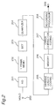
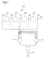
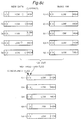
- a detail of the concealment flag detector 120 is shown in Fig. 7.
- the concealment flag detector 120 comprises an input for receiving the concealment flag bit, four shift registers 701, 702, 703 and 704 for producing five subsequent concealment flags including the present concealment flag and the four previous concealment flags, an OR gate 710 for taking an OR of the five subsequent flags, a NAND gate 711 for taking a NAND of the five subsequent flags, and an AND gate 712 for taking an AND between the outputs of the OR gate 710 and NAND gate 711.
- the concealment flag detector 120 receives five concealment flags of one sharing group, it is reset and is ready for receiving next five concealment flags of another sharing group.
- the concealment flag detector 120 detects the following three different situations (i), (ii) and (iii).
- the detected result of the concealment flag detector 120 is applied to HIGH FREQUENCY TRIM (HRT) flag setting circuit 122.
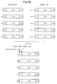
- HRT flag setting circuit 122 maintains the second bit position of the five sync blocks in the sharing group in the reset condition (0), as shown in Figs. 8a and 8c.
- the HRT flag setting circuit 122 sets the second bit position of the five sync blocks in the sharing group to the set condition (1), as shown in Fig. 8b.
- a HIGH FREQUENCY TRIM circuit 124 is coupled with a HIGH FREQUENCY TRIM flag detector 126.
- the HRT flag detector 126 detects set HRT flags, such as in the case of Fig. 8b
- the HIGH FREQUENCY TRIM circuit 124 is activated to trim or cut off the HIGH FREQUENCY data from the sync block. Since the HRT flags are added to all the five sync blocks in one sharing group that has at least one substitute sync block, all the HIGH FREQUENCY data in the five sync blocks in that sharing group are eliminated. When there is one to four substitute sync blocks in one sharing group, the elimination of the HIGH FREQUENCY data is necessary, as explained below.
- the HIGH FREQUENCY data in the substitute sync block may be shifted to the neighbor sync blocks in the sharing group trying to complete the missing part of the HIGH FREQUENCY data in the neighboring sync blocks.
- the HIGH FREQUENCY data in these five sync blocks are cut off.
- the decoding at the bit rate reduction decorder 128 terminates the decoding in response to the 6-th EOB signal.
- the HRT flag detector 126 detects reset HRT flags, such as in the case of Fig. 8a or 8c, the HIGH FREQUENCY TRIM circuit 124 is deactivated to transmit the sync blocks without any change.
- a bit rate reduction decoder 128 receives the sync blocks from the HIGH FREQUENCY TRIM circuit 124 and carries out the variable length code decoding, inverse quantization, and inverse discrete cosine transfer (IDCT) to reproduce the digital video data.
- IDCT inverse discrete cosine transfer
- the number of substituted sync blocks can be minimized, and image deterioration resulting from substitution can be minimized by decoding only the LOW FREQUENCY data of the sync block when one to four sync blocks in one sharing group is substituted by another in the signal processing apparatus according to the present invention.
- block distortion and other image deterioration may occur because the HIGH FREQUENCY data is lost, the resulting visible deterioration in moving image areas is less than that occurring with the loss of block-to-block continuity resulting from substituting a previous block.
- a signal processing apparatus according to the present invention it is possible by applying a signal processing apparatus according to the present invention to display as many blocks as possible on screen.
- bit rate reduction unit is two frames or more, however, less deterioration can be achieved by decoding only the low frequency component of the current page rather than substituting blocks from a past page because of the reduced correlation between the current and past page blocks.
Applications Claiming Priority (2)
| Application Number | Priority Date | Filing Date | Title |
|---|---|---|---|
| JP16720092A JP2962053B2 (ja) | 1992-06-25 | 1992-06-25 | 信号処理装置 |
| JP167200/92 | 1992-06-25 |
Publications (3)
| Publication Number | Publication Date |
|---|---|
| EP0575997A2 true EP0575997A2 (fr) | 1993-12-29 |
| EP0575997A3 EP0575997A3 (en) | 1994-06-08 |
| EP0575997B1 EP0575997B1 (fr) | 1998-09-02 |
Family
ID=15845285
Family Applications (1)
| Application Number | Title | Priority Date | Filing Date |
|---|---|---|---|
| EP19930110060 Expired - Lifetime EP0575997B1 (fr) | 1992-06-25 | 1993-06-24 | Dispositif de traitement de signal d'un enregistreur à cassette vidéo numérique |
Country Status (5)
| Country | Link |
|---|---|
| US (1) | US5392129A (fr) |
| EP (1) | EP0575997B1 (fr) |
| JP (1) | JP2962053B2 (fr) |
| KR (1) | KR100259441B1 (fr) |
| DE (1) | DE69320707T2 (fr) |
Cited By (1)
| Publication number | Priority date | Publication date | Assignee | Title |
|---|---|---|---|---|
| EP0633699A2 (fr) * | 1993-06-30 | 1995-01-11 | Samsung Electronics Co., Ltd. | Méthode de codage intra-image forcé |
Families Citing this family (16)
| Publication number | Priority date | Publication date | Assignee | Title |
|---|---|---|---|---|
| KR0121301B1 (ko) * | 1992-09-30 | 1997-11-17 | 사또오 후미오 | 편집신호 디코딩 장치 |
| US5815636A (en) * | 1993-03-29 | 1998-09-29 | Canon Kabushiki Kaisha | Image reproducing apparatus |
| US6002837A (en) * | 1993-06-30 | 1999-12-14 | Canon Kabushiki Kaisha | Image reproducing apparatus reproducing coded image signals while concealing data which cannot be decoded |
| US5612789A (en) * | 1993-09-03 | 1997-03-18 | Sony Corporation | Video signal recorder and video apparatus with internal clock index signal |
| JPH0795538A (ja) * | 1993-09-17 | 1995-04-07 | Canon Inc | 画像記録再生装置 |
| JPH07282549A (ja) * | 1994-04-12 | 1995-10-27 | Kodo Eizo Gijutsu Kenkyusho:Kk | 圧縮画像データ記録再生装置 |
| JPH08212713A (ja) * | 1995-02-03 | 1996-08-20 | Sony Corp | データレコーダー |
| JP3155952B2 (ja) * | 1995-05-22 | 2001-04-16 | 株式会社エヌ・ティ・ティ・ドコモ | 音声復号装置 |
| KR0165439B1 (ko) * | 1995-09-14 | 1999-03-20 | 김광호 | 디지탈 비디오 테이프 레코더의 화면 구성 장치 및 방법 |
| US6052415A (en) * | 1997-08-26 | 2000-04-18 | International Business Machines Corporation | Early error detection within an MPEG decoder |
| JP4066576B2 (ja) * | 1999-10-26 | 2008-03-26 | ソニー株式会社 | データ再生装置及び方法 |
| US7159164B1 (en) | 2000-06-05 | 2007-01-02 | Qualcomm Incorporated | Method and apparatus for recovery of particular bits of a frame |
| US6728318B2 (en) | 2001-03-02 | 2004-04-27 | Redrock Semiconductor, Ltd. | Error recovery of corrupted MPEG-4 bitstreams using fuzzy decoding of start codes and resync markers |
| JP4562520B2 (ja) * | 2004-12-28 | 2010-10-13 | 富士通テン株式会社 | デジタルデータ受信機 |
| CN101346759B (zh) | 2005-12-21 | 2011-09-07 | 日本电气株式会社 | 代码转换装置、用于代码转换装置的代码转换方法及程序 |
| US8687301B1 (en) * | 2013-01-08 | 2014-04-01 | Lsi Corporation | Parallel no-sync-mark retry |
Citations (6)
| Publication number | Priority date | Publication date | Assignee | Title |
|---|---|---|---|---|
| EP0203773A2 (fr) * | 1985-05-21 | 1986-12-03 | Sony Corporation | Appareil de décodage d'un code de correction d'erreurs |
| EP0470772A2 (fr) * | 1990-08-09 | 1992-02-12 | Matsushita Electric Industrial Co., Ltd. | Dispositif de reproduction de signal vidéo digital |
| EP0471580A2 (fr) * | 1990-08-16 | 1992-02-19 | Matsushita Electric Industrial Co., Ltd. | Méthode de masquage pour signal vidéo |
| EP0517141A2 (fr) * | 1991-06-04 | 1992-12-09 | Kabushiki Kaisha Toshiba | Dispositif de traitement de signal à haute efficacité de codage avec réduction de l'influence de propagation d'erreurs |
| EP0527611A2 (fr) * | 1991-08-09 | 1993-02-17 | Sony Corporation | Dispositif d'enregistrement de signal vidéo numérique |
| EP0546691A2 (fr) * | 1991-11-12 | 1993-06-16 | Samsung Electronics Co. Ltd. | Enregistrement et réproduction numériques |
Family Cites Families (11)
| Publication number | Priority date | Publication date | Assignee | Title |
|---|---|---|---|---|
| BE890517A (fr) * | 1981-09-28 | 1982-01-18 | Staar Sa | Dispositif de memorisation d'images electroniques |
| GB2121642B (en) * | 1982-05-26 | 1985-11-27 | Sony Corp | Error concealment in digital television signals |
| US5032927A (en) * | 1988-03-01 | 1991-07-16 | Fuji Photo Film Co., Ltd. | Image signal recording apparatus capable of recording compressed image data together with audio data |
| JP3050553B2 (ja) * | 1988-04-08 | 2000-06-12 | ソニー株式会社 | データ再生装置 |
| JPH0787013B2 (ja) * | 1988-10-26 | 1995-09-20 | ティアツク株式会社 | ドロップアウト検出回路 |
| JP3018366B2 (ja) * | 1989-02-08 | 2000-03-13 | ソニー株式会社 | ビデオ信号処理回路 |
| US5193010A (en) * | 1989-08-29 | 1993-03-09 | Matsushita Electric Industrial Co., Ltd. | Digital video signal recording and reproducing apparatus having an error concealment control function |
| US5142380A (en) * | 1989-10-23 | 1992-08-25 | Ricoh Company, Ltd. | Image data processing apparatus |
| JPH04140084A (ja) * | 1990-09-28 | 1992-05-14 | Copal Electron Co Ltd | 直流モータ起動不良検出回路 |
| JPH05114251A (ja) * | 1991-10-23 | 1993-05-07 | Matsushita Electric Ind Co Ltd | 誤り修整方法 |
| JPH04271071A (ja) * | 1991-02-26 | 1992-09-28 | Matsushita Electric Ind Co Ltd | 誤り修整方法 |
-
1992
- 1992-06-25 JP JP16720092A patent/JP2962053B2/ja not_active Expired - Fee Related
-
1993
- 1993-06-24 EP EP19930110060 patent/EP0575997B1/fr not_active Expired - Lifetime
- 1993-06-24 KR KR1019930011565A patent/KR100259441B1/ko not_active IP Right Cessation
- 1993-06-24 DE DE1993620707 patent/DE69320707T2/de not_active Expired - Fee Related
- 1993-06-25 US US08/083,052 patent/US5392129A/en not_active Expired - Lifetime
Patent Citations (6)
| Publication number | Priority date | Publication date | Assignee | Title |
|---|---|---|---|---|
| EP0203773A2 (fr) * | 1985-05-21 | 1986-12-03 | Sony Corporation | Appareil de décodage d'un code de correction d'erreurs |
| EP0470772A2 (fr) * | 1990-08-09 | 1992-02-12 | Matsushita Electric Industrial Co., Ltd. | Dispositif de reproduction de signal vidéo digital |
| EP0471580A2 (fr) * | 1990-08-16 | 1992-02-19 | Matsushita Electric Industrial Co., Ltd. | Méthode de masquage pour signal vidéo |
| EP0517141A2 (fr) * | 1991-06-04 | 1992-12-09 | Kabushiki Kaisha Toshiba | Dispositif de traitement de signal à haute efficacité de codage avec réduction de l'influence de propagation d'erreurs |
| EP0527611A2 (fr) * | 1991-08-09 | 1993-02-17 | Sony Corporation | Dispositif d'enregistrement de signal vidéo numérique |
| EP0546691A2 (fr) * | 1991-11-12 | 1993-06-16 | Samsung Electronics Co. Ltd. | Enregistrement et réproduction numériques |
Non-Patent Citations (1)
| Title |
|---|
| IEEE TRANSACTIONS ON CONSUMER ELECTRONICS, vol. 37, no. 3, August, 1991, New York, US, XP000263194, pages 261-265; C. YAMAMITSU et al.: 'A study on trick * |
Cited By (2)
| Publication number | Priority date | Publication date | Assignee | Title |
|---|---|---|---|---|
| EP0633699A2 (fr) * | 1993-06-30 | 1995-01-11 | Samsung Electronics Co., Ltd. | Méthode de codage intra-image forcé |
| EP0633699A3 (fr) * | 1993-06-30 | 1995-04-05 | Samsung Electronics Co Ltd | Méthode de codage intra-image forcé. |
Also Published As
| Publication number | Publication date |
|---|---|
| DE69320707T2 (de) | 1999-01-21 |
| KR940006118A (ko) | 1994-03-23 |
| EP0575997B1 (fr) | 1998-09-02 |
| EP0575997A3 (en) | 1994-06-08 |
| KR100259441B1 (ko) | 2000-06-15 |
| DE69320707D1 (de) | 1998-10-08 |
| JP2962053B2 (ja) | 1999-10-12 |
| US5392129A (en) | 1995-02-21 |
| JPH0614294A (ja) | 1994-01-21 |
Similar Documents
| Publication | Publication Date | Title |
|---|---|---|
| EP0533947B1 (fr) | Codeur et decodeur | |
| KR960002393B1 (ko) | 영상신호기록재생장치 | |
| US5550640A (en) | Digital video signal recording and reproducing apparatus and method for setting a number of compression blocks according to different operational modes | |
| JP3134424B2 (ja) | 可変長符号化方法及び装置 | |
| US5392129A (en) | Digital VCR signal processing apparatus for concealing uncorrectable errors | |
| EP0617558B1 (fr) | Appareil pour dissimuler des erreurs de données | |
| JP2708312B2 (ja) | 記録装置及び再生装置 | |
| JPH0983951A (ja) | 画像符号化記録再生装置 | |
| US5122876A (en) | Image signal restoring apparatus | |
| EP0644691B1 (fr) | Appareils d'enregistrement et de reproduction de signaux vidéo comprimés | |
| EP0602817B1 (fr) | Dispositif de traitement d'un signal vidéo numérique | |
| US5101274A (en) | Digital signal recording apparatus time-division multiplexing video and audio signals | |
| EP0553817B1 (fr) | Appareil de transfert d'informations digitales | |
| US6219157B1 (en) | Image coding apparatus | |
| US6009227A (en) | HDTV digital recorder with compressed image data inserted in a video signal that corresponds to a video interface standard | |
| US20060062309A1 (en) | Coding/decoding apparatus | |
| JP3207739B2 (ja) | 画像再生装置 | |
| US6301390B1 (en) | Encoding image data in blocks read out in a predetermined order | |
| US6208803B1 (en) | Recording and/or reproducing apparatus which produces main information and historical information with respect to signal processing performed on the main information | |
| JP3291785B2 (ja) | ブロック変換符号化データの伝送装置 | |
| JP3106479B2 (ja) | ディジタルコンポーネント信号の記録装置及び記録方法 | |
| JP3158603B2 (ja) | ディジタル画像信号の伝送装置 | |
| JP3063675B2 (ja) | 映像信号の再生装置 | |
| JPH06302125A (ja) | ディジタル信号処理装置 | |
| JPH05292459A (ja) | ディジタル映像信号の記録装置 |
Legal Events
| Date | Code | Title | Description |
|---|---|---|---|
| PUAI | Public reference made under article 153(3) epc to a published international application that has entered the european phase |
Free format text: ORIGINAL CODE: 0009012 |
|
| 17P | Request for examination filed |
Effective date: 19930624 |
|
| AK | Designated contracting states |
Kind code of ref document: A2 Designated state(s): DE FR GB NL |
|
| PUAL | Search report despatched |
Free format text: ORIGINAL CODE: 0009013 |
|
| AK | Designated contracting states |
Kind code of ref document: A3 Designated state(s): DE FR GB NL |
|
| 17Q | First examination report despatched |
Effective date: 19961230 |
|
| GRAG | Despatch of communication of intention to grant |
Free format text: ORIGINAL CODE: EPIDOS AGRA |
|
| GRAG | Despatch of communication of intention to grant |
Free format text: ORIGINAL CODE: EPIDOS AGRA |
|
| GRAH | Despatch of communication of intention to grant a patent |
Free format text: ORIGINAL CODE: EPIDOS IGRA |
|
| GRAH | Despatch of communication of intention to grant a patent |
Free format text: ORIGINAL CODE: EPIDOS IGRA |
|
| GRAA | (expected) grant |
Free format text: ORIGINAL CODE: 0009210 |
|
| AK | Designated contracting states |
Kind code of ref document: B1 Designated state(s): DE FR GB NL |
|
| REF | Corresponds to: |
Ref document number: 69320707 Country of ref document: DE Date of ref document: 19981008 |
|
| ET | Fr: translation filed | ||
| PLBE | No opposition filed within time limit |
Free format text: ORIGINAL CODE: 0009261 |
|
| STAA | Information on the status of an ep patent application or granted ep patent |
Free format text: STATUS: NO OPPOSITION FILED WITHIN TIME LIMIT |
|
| 26N | No opposition filed | ||
| REG | Reference to a national code |
Ref country code: GB Ref legal event code: IF02 |
|
| PGFP | Annual fee paid to national office [announced via postgrant information from national office to epo] |
Ref country code: NL Payment date: 20070617 Year of fee payment: 15 |
|
| PGFP | Annual fee paid to national office [announced via postgrant information from national office to epo] |
Ref country code: DE Payment date: 20070621 Year of fee payment: 15 |
|
| PGFP | Annual fee paid to national office [announced via postgrant information from national office to epo] |
Ref country code: GB Payment date: 20070620 Year of fee payment: 15 |
|
| PGFP | Annual fee paid to national office [announced via postgrant information from national office to epo] |
Ref country code: FR Payment date: 20070608 Year of fee payment: 15 |
|
| GBPC | Gb: european patent ceased through non-payment of renewal fee |
Effective date: 20080624 |
|
| NLV4 | Nl: lapsed or anulled due to non-payment of the annual fee |
Effective date: 20090101 |
|
| REG | Reference to a national code |
Ref country code: FR Ref legal event code: ST Effective date: 20090228 |
|
| PG25 | Lapsed in a contracting state [announced via postgrant information from national office to epo] |
Ref country code: DE Free format text: LAPSE BECAUSE OF NON-PAYMENT OF DUE FEES Effective date: 20090101 |
|
| PG25 | Lapsed in a contracting state [announced via postgrant information from national office to epo] |
Ref country code: NL Free format text: LAPSE BECAUSE OF NON-PAYMENT OF DUE FEES Effective date: 20090101 |
|
| PG25 | Lapsed in a contracting state [announced via postgrant information from national office to epo] |
Ref country code: GB Free format text: LAPSE BECAUSE OF NON-PAYMENT OF DUE FEES Effective date: 20080624 |
|
| PG25 | Lapsed in a contracting state [announced via postgrant information from national office to epo] |
Ref country code: FR Free format text: LAPSE BECAUSE OF NON-PAYMENT OF DUE FEES Effective date: 20080630 |