EP0565035B9 - Optical modulator optical transmitter apparatus and optical transmission system - Google Patents
Optical modulator optical transmitter apparatus and optical transmission system Download PDFInfo
- Publication number
- EP0565035B9 EP0565035B9 EP93105624A EP93105624A EP0565035B9 EP 0565035 B9 EP0565035 B9 EP 0565035B9 EP 93105624 A EP93105624 A EP 93105624A EP 93105624 A EP93105624 A EP 93105624A EP 0565035 B9 EP0565035 B9 EP 0565035B9
- Authority
- EP
- European Patent Office
- Prior art keywords
- optical
- signal
- modulator
- phase
- intensity
- Prior art date
- Legal status (The legal status is an assumption and is not a legal conclusion. Google has not performed a legal analysis and makes no representation as to the accuracy of the status listed.)
- Expired - Lifetime
Links
Images


Classifications
-
- B—PERFORMING OPERATIONS; TRANSPORTING
- B82—NANOTECHNOLOGY
- B82Y—SPECIFIC USES OR APPLICATIONS OF NANOSTRUCTURES; MEASUREMENT OR ANALYSIS OF NANOSTRUCTURES; MANUFACTURE OR TREATMENT OF NANOSTRUCTURES
- B82Y20/00—Nanooptics, e.g. quantum optics or photonic crystals
-
- H—ELECTRICITY
- H04—ELECTRIC COMMUNICATION TECHNIQUE
- H04B—TRANSMISSION
- H04B10/00—Transmission systems employing electromagnetic waves other than radio-waves, e.g. infrared, visible or ultraviolet light, or employing corpuscular radiation, e.g. quantum communication
- H04B10/25—Arrangements specific to fibre transmission
- H04B10/2507—Arrangements specific to fibre transmission for the reduction or elimination of distortion or dispersion
- H04B10/2537—Arrangements specific to fibre transmission for the reduction or elimination of distortion or dispersion due to scattering processes, e.g. Raman or Brillouin scattering
-
- G—PHYSICS
- G02—OPTICS
- G02F—OPTICAL DEVICES OR ARRANGEMENTS FOR THE CONTROL OF LIGHT BY MODIFICATION OF THE OPTICAL PROPERTIES OF THE MEDIA OF THE ELEMENTS INVOLVED THEREIN; NON-LINEAR OPTICS; FREQUENCY-CHANGING OF LIGHT; OPTICAL LOGIC ELEMENTS; OPTICAL ANALOGUE/DIGITAL CONVERTERS
- G02F1/00—Devices or arrangements for the control of the intensity, colour, phase, polarisation or direction of light arriving from an independent light source, e.g. switching, gating or modulating; Non-linear optics
- G02F1/01—Devices or arrangements for the control of the intensity, colour, phase, polarisation or direction of light arriving from an independent light source, e.g. switching, gating or modulating; Non-linear optics for the control of the intensity, phase, polarisation or colour
- G02F1/015—Devices or arrangements for the control of the intensity, colour, phase, polarisation or direction of light arriving from an independent light source, e.g. switching, gating or modulating; Non-linear optics for the control of the intensity, phase, polarisation or colour based on semiconductor elements having potential barriers, e.g. having a PN or PIN junction
- G02F1/017—Structures with periodic or quasi periodic potential variation, e.g. superlattices, quantum wells
- G02F1/01708—Structures with periodic or quasi periodic potential variation, e.g. superlattices, quantum wells in an optical wavequide structure
-
- G—PHYSICS
- G02—OPTICS
- G02F—OPTICAL DEVICES OR ARRANGEMENTS FOR THE CONTROL OF LIGHT BY MODIFICATION OF THE OPTICAL PROPERTIES OF THE MEDIA OF THE ELEMENTS INVOLVED THEREIN; NON-LINEAR OPTICS; FREQUENCY-CHANGING OF LIGHT; OPTICAL LOGIC ELEMENTS; OPTICAL ANALOGUE/DIGITAL CONVERTERS
- G02F2203/00—Function characteristic
- G02F2203/25—Frequency chirping of an optical modulator; Arrangements or methods for the pre-set or tuning thereof
Definitions
- the present invention relates generally to an optical signal transmission using an optical fiber and more particularly to an optical transmitter as well as an optical signal transmission system which are suited advantageously for digital optical communication.
- an external modulation system i.e., a system for modulating a light beam of a constant intensity or power emitted from a laser with an optical intensity modulator
- a hitherto known direct modulation system i.e., a system for modulating the intensity of light beam by modulating a current for driving the laser. This is primarily for the reason that the external modulation system is less susceptible to the chirping.
- stimulated Brillouin scattering which is one of the non-linear optical effects is more likely to take place as spectrum spreading of the light source becomes smaller.
- the stimulated Brillouin scattering takes place, incurring rapid attenuation of the light signal propagating or travelling through the optical fiber.
- the measures for coping with the stimulated Brillouin scattering due to the spectrum spreading is naturally in conflict with the measures for reducing the chirping of the light source. Accordingly, there exists a great demand for a method or technology which can solve both the problems mentioned above simultaneously in a satisfactory manner.
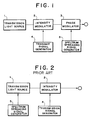
- Fig. 2 shows a structure of an optical transmitter implemented on the basis of the technology disclosed in the above-mentioned literature.
- a light beam emitted from a light source 1 for signal transmission undergoes intensity modulation in an intensity modulator 2 in accordance with a signal to be transmitted (hereinafter referred to also as the transmit signal or transmission signal) generated by a transmit signal generator 4 before being transmitted through an optical fiber.
- the transmit signal or transmission signal a signal to be transmitted
- direct frequency modulation is effected for the light source 1 with a signal generated by a signal generator 5 for thereby spreading the spectrum of the light beam emitted from the light source 1.
- the optical signal having spread spectrum suffers from jitter under the influence of dispersion which the optical signal undergoes in the course of propagation through the optical fiber.
- the time jitter can be estimated smaller than 14 ps when the modulating frequency is set higher than 10 kHz with frequency deviation being within 1 GHz for a transmission fiber exhibiting a total dispersion of 1800 ps/nm.
- the prior art technique described above suffers from problems that a driver circuit of complicated configuration is required for the direct frequency modulation of the light source in order to spread the spectrum of the light beam for signal transmission and that variation in the light intensity can not be avoided.
- JP-A-4-014 010 discloses an optical transmitter apparatus with the features included in the first part of claim 1.
- the document deals with suppressing frequency chirping of an external optical modulator rather than effects of stimulated Brillouin scattering.
- An intensity modulator and a phase modulator are cascaded, and the same electrical signal, which is varied in level, is applied to the phase modulator and, with a certain delay, to the intensity modulator.
- a light beam emitted from the light source undergoes intensity modulation by the intensity modulator and phase modulation by the phase modulator, whereby spectrum of the optical signal is spread, which is effective for suppressing the stimulated Brillouin scattering while avoiding variation in the intensity due to the spectrum spreading.
- optical coupler elements which will otherwise be required for coupling these optical elements can be spared, which in turn means that the optical transmitter apparatus can be realized in a simplified structure of a reduced size.
- Fig. 1 shows schematically a general configuration of an optical transmitter apparatus according to a first embodiment of the present invention.
- a light beam for optical signal transmission is emanated from a light source 1 for signal transmission and caused to pass through an intensity modulator 2 and a phase modulator 3.
- a signal to be transmitted is generated by a transmit signal generator 4 and inputted to the intensity modulator 3, while a spectrum spreading signal generated by a spectrum spreading signal generator 5 is inputted to the phase modulator 3.
- the light beam emitted from the light source 1 undergoes intensity modulation in the intensity modulator 2 in accordance with the signal supplied from the transmit signal generator 4, whereby an intensity modulated optical signal is generated as the optical signal to be transmitted through an optical fiber.
- the optical signal outputted from the intensity modulator 3 undergoes a phase modulation upon passing through the phase modulator 3 in accordance with the spectrum spreading signal generated by the spectrum spreading signal generator 5, whereby spectrum of the optical signal is spread.
- the optical signal outputted from the optical transmitter apparatus shown in Fig. 1 is protected against the stimulated Brillouin scattering.
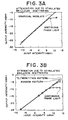
- Figs. 3A and 3B graphically illustrate results of an experiment performed for confirming the effects obtained according to the instant embodiment of the invention for an optical signal transmitted through a single mode dispersion shifted fiber having a length of 60 km.
- input intensity of the optical signal inputted to the optical fiber is taken along the abscissa, while the output intensity of the optical signal upon leaving the fiber is taken along the ordinate.
- Fig. 3A shows the result of the experiment in which a sinusoidal signal was employed as the spectrum spreading signal
- Fig. 3B shows the results obtained by employing a rectangular signal as the spectrum spreading signal.
- measurement was also performed by using a continuous phase optical signal as the spectrum spreading signal.
- the phase modulation with a rectangular signal of a random pattern is more effective for spectrum spreading and hence for suppressing the influence of the stimulated Brillouin scattering when compared with the phase modulation by using a rectangular signal of a regular pattern typified by a "1, 0"-repetition pattern.
- the results of the experiments shows that the spreading of spectrum by modulating the phase of the optical signal is effective for suppressing the stimulated Brillouin scattering.
- the waveform of the spectrum spreading signal is neither limited to the sinusoidal waveform nor the rectangular waveform. Any other suitable waveforms can be employed to this end.
- the order in which the light beam or the optical signal is inputted to the intensity modulator 2 and the phase modulator 3 presents practically no problem.
- the aimed effect can equally be obtained even when the signal input sequence is changed such that the light beam emitted by the light source 1 is first inputted to the phase modulator 3 and then the output optical signal of the latter is inputted to the intensity modulator 2.
- phase modulator 3 As typical elements which can be employed as the phase modulator 3, there may be mentioned those made of a semiconductor material such as gallium arsenide or lithium niobate (LiNbO 3 ), by way of example.
- intensity modulator 2 there may be employed an electro-absorption type intensity modulator or a Mach-Zehnder type intensity modulator which can be implemented by a combination of two phase modulators.
- both the intensity modulator 2 and the phase modulator 3 can be realized by using a same material, both modulators can easily be implemented in an integrated structure.
- An embodiment of the invention in which an optical element realized by integrating the intensity modulator and the phase modulator with each other is employed will be described below.
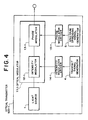
- Fig. 4 shows a configuration of an optical transmitter apparatus 100-1 according to a second embodiment of the invention in which an electroabsorption type intensity modulator is integrally combined with a semiconductor phase modulator.
- a light beam emitted from a light source 1 for signal transmission is inputted to an optical modulator 11-1.
- a signal for transmission which is generated by a transmit signal generator 4 is inputted to an intensity modulator driver circuit 14-1, whose output signal is applied to an intensity modulator element 12-1 incorporated in the optical modulator 11-1.
- the output signal of the intensity modulator driver circuit 14-1 is an electric signal having a predetermined voltage or current level which is sufficiently high for modulating the intensity of the light beam inputted to the optical modulator 11-1.
- a reference numeral 5 denotes a spectrum spreading signal generator, whose output signal is inputted to a phase modulator driver circuit 15-1, the output signal of which in turn is applied to a phase modulator element 13-1 incorporated in the optical modulator 11-1 for modulating phase of the optical signal outputted from the intensity modulator element 12-1.
- the output signal of the phase modulator driver circuit 15-1 is an electric signal having a predetermined voltage or current level which is sufficiently high to spread the spectrum of the optical signal outputted from the intensity modulator element 12-1.
- the light beam inputted to the optical modulator 11-1 undergoes an intensity modulation by the intensity modulator element 12-1 and then a spectrum spreading operation of the phase modulator element 13-1 to be finally sent out from the optical transmitter apparatus 100-1. Because the optical signal as sent out has a spectrum spread, the stimulated Brillouin scattering can effectively be suppressed.
- the optical modulator 11-1 can easily be implemented in an integral structure by manufacturing the intensity modulator element 12-1 and the phase modulator element 13-1 from semiconductor materials belonging to a same series. By integrating both the elements in this way, loss of light at the coupling interface between the intensity modulator element 12-1 and the phase modulator element 13-1 can satisfactorily be prevented. Besides, there can be spared any optical coupler which will otherwise be required for optically coupling the elements 12-1 and 13-1.
- the order in which the light beam and the optical signal are inputted to the intensity modulator element 12-1 and the phase modulator element 13-1 may be reversed relative to the order shown in Fig. 4, to essentially same effects.
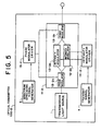
- Fig. 5 shows an optical transmitter apparatus according to a third embodiment of the present invention in which a Mach-Zehnder type intensity modulator constituted by a combination of two phase modulators is combined with a phase modulator in an integral structure.
- a light beam emitted from a light source 1 is inputted to an optical modulator 11-2.
- a signal for transmission is generated by a transmit signal generator 4 and inputted to an intensity modulator driver circuit 14-2 which produces two output signals. These output signals are then inputted to intensity modulator elements 12-2a and 12-2b, respectively, which are incorporated in the optical intensity modulator 11-2.
- Each of the outputs of the intensity modulator driver circuit 14-2 is an electric signal having a predetermined voltage or current level which renders the optical phase difference between the optical signals passing through the intensity modulator elements 12-2a and 12-2b, respectively, to be zero or 180 degrees.
- the optical output of the Mach-Zehnder type intensity modulator assumes a maximum level, when the phase difference between the optical signals passing through the optical modulating elements 12-2a and 12-2b, respectively, is zero degree while assuming a minimum value due to interference when the above-mentioned phase difference is 180 degree.
- a spectrum spreading signal generated by a spectrum spreading signal generator 5 is inputted to a phase modulator driver circuit 15-2, whose output signal is supplied to phase modulator elements 13-2a and 13-2b, respectively, which are equally incorporated in the optical modulator 11-2.
- the output of the phase modulator driver circuit 15-2 is also an electric signal having a predetermined voltage or current level capable of modulating the phase of the light beam and the optical signal passing through the phase modulator elements 13-2a and 13-2b, respectively.
- the light beam inputted to the optical modulator 11-2 is modulated in respect to the intensity by the intensity modulator elements 12-2a and 12-2b, while being spread in spectrum by the phase modulator elements 13-2a and 13-2b, to be finally sent out from the optical transmitter 100-2.
- the optical signal as sent out is scarcely affected by the stimulated Brillouin scattering because of the spectrum being spread.
- the optical modulator 11-2 can easily be realized in an integral structure by manufacturing the intensity modulator elements 12-2a, 12-2b and the phase modulator elements 13-2a, 13-2b from semiconductor materials of a same series such as lithium niobate. Owing to the integration, optical loss at the coupling interfaces between the intensity modulator elements 12-2a, 12-2b and the phase modulator elements 13-2a, 13-2b can be reduced. Besides, optical coupling elements which will otherwise be required can be spared.
- phase modulator is separated into two phase modulator elements 13-2a and 13-2b.
- the intensity modulator elements 12-2a and 12-2b are combined with either one of the phase modulator element 13-2a of the preceding stage or the phase modulator element 13-2b of the succeeding stage.
- Fig. 6 shows an optical transmitter apparatus according to a fourth embodiment of the present invention in which a Mach-Zehnder type intensity modulator constituted by a combination of two phase modulators is designed to serve also for the function of a phase modulator.
- a light beam emitted from a light source 1 is inputted to an optical modulator 11-3.
- a signal to be transmitted as generated by a transmit signal generator 4 and a signal generated by a spectrum spreading signal generator 5 are inputted to an intensity modulator driver circuit 14-3, in which both input signals are combined by voltage combine circuits 6-a and 6-b, the outputs of which are then applied to intensity modulator elements 12-3a and 12-3b, respectively.
- the signal for transmission as generated by the transmit signal generator 4 is applied to the input of the voltage combine circuit 6-a as a voltage signal of positive (plus) polarity, while being applied to the input of the voltage combine circuit 6-b as a voltage signal of negative (minus) polarity, to thereby render the optical phase difference of the optical signal between the intensity modulator elements 12-3a and 12-3b to be zero or 180 degrees.
- the signal outputted from the spectrum spreading signal generator 5 is applied to the inputs of both voltage combine circuits 6-a and 6-b as a voltage signal of positive polarity to make effective an in-phase modulation in the intensity modulator elements 12-3a and 12-3b.
- the light beam inputted to the optical modulator 11-3 is modulated in intensity and phase and spread in spectrum, to be finally sent out from the optical transmitter apparatus 100-3.
- the optical signal as sent out is effectively protected against influence of the stimulated Brillouin scattering.
- the optical modulator 11-3 is constituted only by the intensity modulator elements 12-3a and 12-3b, the number of optical parts as required can be reduced, to another advantage.
- Fig. 7 shows a circuit configuration of an optical transmitter apparatus according to a fifth embodiment of the invention in which a Mach-Zehnder type intensity modulator constituted by a combination of two phase modulators is employed.
- a light beam emitted from a transmission light source 1 is inputted to an optical modulator 11-4.
- a transmit signal to be transmitted as generated by a transmit signal generator 4 is inputted to a digital logic circuit 16.
- Digital signals 17-a and 17-b outputted from the digital logic circuit 16 as a result of logical processing of the transmit signal are inputted to intensity modulator driver circuits 14-4a and 14-4b, respectively.
- the output signals of these two driver circuits 14-4a and 14-4b are inputted to intensity modulator elements 12-4a and 12-4b, respectively, which constitute the optical modulator 11-4.
- the optical signals inputted to the optical modulator 11-4 undergoes intensity modulation and phase modulation through the intensity modulator element 12-4a and 12-4b, respectively, to be sent out from the optical transmitter apparatus 100-4 with spread spectrum being spread.
- the digital signals 17-a and 17-b which are delivered from the two outputs, respectively, of the digital logic circuit 16 assume values "0" and "1".
- the output of the intensity modulator driver circuit 14-4a assumes a level of "V-", whereby the phase of the light beam passing through the intensity modulator element 12-4a is caused to advance by 90° from a reference phase.
- the output of the intensity modulator driver circuit 14-4a assumes a level of "V+", whereby the phase of the light beam passing through the intensity modulator element 12-4a is delayed by 90° relative to the reference phase.
- the output of the intensity modulator driver circuit 14-4b assumes the level of "V-" or "V+”, as a result of which the phase of the light beam passing through the intensity modulator element 12-4b is caused to advance or delay by 90° relative to the reference phase.
- intensity and phase of the optical signal outputted from the optical modulator 11-4 undergoes modulations, as mentioned below.
- operation or function of the digital logic circuit 16 is as follows.
- combination of the digital signals 17-a and 17-b generated by the digital logic circuit 16 is represented by “0, 1" or “1, 0".
- the digital logic circuit 16 when the signal supplied from the transmit signal generator 4 is "1", the digital logic circuit 16 generates combinations of digital signals 17-a and 17-b in an alternating, random or predetermined sequence of "0, 0" and "1, 1".
- phase of the optical signal as outputted is correspondingly modulated with the spectrum thereof being spread, which is effective for suppressing the stimulated Brillouin scattering.
- the optical modulator 11-4 is constituted only by the intensity modulator elements 12-4a and 12-4b, the number of components required for implementation of the optical signal transmitter apparatus according to the instant embodiment can be decreased, to further advantage.
- Fig. 8A shows, by way of example, a circuit configuration of the digital logic circuit 16.
- the digital logic circuit 16 is comprised of two T flip-flops 18-a and 18-b, wherein the signal to be transmitted is inputted to each of these T flip-flops 18-a and 18-b, whereby corresponding output signals 17-a and 17-b are generated by these T flip-flops 18-a and 18-b, respectively.
- the input signal for transmission is a digital signal of NRZ code (non-return-to-zero code), as shown in Fig. 8B at a row 1.
- NRZ code non-return-to-zero code
- the T flip-flop 18-a is triggered in response to a rise-up edge of the input signal to thereby produce an output signal having a waveform such as illustrated in Fig. 8B at a row 2.
- the T flip-flop 18-b is triggered in response to a falling edge of the input signal to produce an output signal having such a waveform as shown in Fig. 8B at a row 3.
- Fig. 9A shows another exemplary configuration of the digital logic circuit 16.
- a signal for transmission i.e., transmit signal
- a signal for transmission is inputted to two logic gates 19-a and 19-b, whereby two output signals 17-a and 17-b are outputted from these logic gates 19-a and 19-b, respectively.
- Fig. 9B illustrates waveforms of the input signal and the output signals of the digital logic gates.
- a reference numeral 20 denotes a digital random signal generator whose output signal is inputted to the aforementioned two digital logic gates 19-a and 19-b.
- the output signals 17-a and 17-b are combined such that these outputs assume a combination of "0, 0" when the input signal is “0", while-assuming a combination of "0, 0” or “1, 1” in dependence on the signal outputted from the digital random signal generator 20.
- the digital random signal generator 20 employed in this embodiment may be so designed as to generate "0" and "1” alternately with each other or generate "0" and “1” mixed in accordance with a predetermined rule. In any case, the stimulated Brillouin scattering can effectively be suppressed.
- the timing at which the output signal of the digital random signal generator 20 should desirably coincide with the timing of the transmit signal. Accordingly, there is conceived such arrangement in which a clock signal employed for controlling the transmit signal generator or alternatively the transmit signal itself is employed as a trigger signal, although illustration of a concrete circuit configuration to this end is omitted.
- a Mach-Zehnder type modulator is employed in the optical signal transmitter apparatuses according to the fourth and fifth embodiments.
- the Mach-Zehnder type modulator however suffers from a problem that extinction ratio is degraded due to difference in the refractive index and the optical path length between the two intensity modulator elements constituting the Mach-Zehnder type modulator.
- the problem of degradation of the extinction ratio can be solved by compensating for the effective optical path length by applying a bias signal to the two outputs of the intensity modulator driver circuit 14-2 or 14-3.
- Fig. 10 shows schematically a structure of an optical signal transmission system in which one of the optical transmitter apparatuses according to the first to fifth embodiments of the invention is employed.
- the optical signal transmission system illustrated is comprised of one optical signal transmitter 100, at least one optical fiber 101 for signal transmission, optical amplifiers 102 and an optical signal receiver 103.
- Output signal of the optical transmitter 100 is inputted to the optical fiber 101.
- the output signal from the optical fiber 101 is inputted straightforwardly to the optical receiver 103.
- the output signal of one optical fiber is once amplified by the optical amplifier 102 and inputted to a succeeding optical fiber 101.
- the output of the last optical fiber is inputted to the optical receiver 103.
- the former can be transmitted to the optical receiver 103 without undergoing adverse influence of the stimulated Brillouin scattering in the course of propagation through the optical fiber.
- Fig. 11 shows schematically a structure of an optical transmission system according to a further embodiment of the invention in which one of the optical transmitters described hereinbefore in conjunction with the first to fifth embodiments can be employed.
- the optical transmission system according to the instant embodiment is comprised of a wavelength division multiplex optical transmitter unit 110 which includes a plurality of optical transmitters 111-1 to 111-n (denoted generally by 111-(1 ⁇ n)) and an optical wavelength multiplexer 112, at least one optical transmission fiber 110 and an optical amplifier(s) 102, and a wavelength division multiplex optical receiver apparatus 113 which includes an optical wavelength demultiplexer 114 and a plurality of optical receivers 115-5 to 115-n (denoted generally by 115-(1 ⁇ n)).
- the outputs of the individual optical transmitters 111-(1 ⁇ n) are inputted to the optical wavelength multiplexer 112 to be multiplexed into an optical signal which is outputted from the wavelength division multiplex optical transmitter unit 110 as the output signal thereof, which is then inputted to the optical fiber 101.
- the output signal leaving the serial optical fiber 101 is inputted straightforwardly to the wavelength division multiplex receiver apparatus 113.
- the output signal of the optical fiber 101 is first amplified by the optical amplifier 102 before being inputted to the wavelength division multiplex optical receiver apparatus 113.
- the optical signal inputted to the wavelength division multiplex optical receiver apparatus 113 is applied to the input of the optical wavelength demultiplexer 114, and a plurality of optical signal outputs resulting from the demultiplexing operation of the demultiplexer 114 are inputted to the optical receivers 115-(1 ⁇ n), respectively, to be received thereby.
- the optical signal outputted from the wavelength division multiplex transmitter unit 110 has spectrum spread by the optical transmitters 111-(1 ⁇ n), the optical signal can reach the wavelength division multiplex receiver apparatus 113 without suffering the influence of the stimulated Brillouin scattering in the course of propagation through the optical fiber 101.
- the optical wavelength multiplexer 112 may be replaced by an optical coupler, to substantially same advantageous effects.
- a structure of this modification is shown in Fig. 12, in which the optical coupler is denoted by a numeral 116.
- the optical signal for transmission which is phase-modulated in the optical transmitter apparatus 100 described hereinbefore in conjunction with the first to fourth embodiments of the invention suffers time jitter upon reception under the influence of dispersion of wavelength during the transmission through the optical fiber.
- Fig. 13 shows schematically a further embodiment of the invention according to which a clock control is adopted in the optical transmitter apparatus of the first embodiment.
- the output signal of the spectrum spreading signal generator 5 is inputted to a clock generator circuit 21 which constitutes a part of the transmit signal generator 4.
- the output of the clock generator circuit 21 is inputted to a data generator circuit 22.
- the optical signal phase-modulated in accordance with the output signal of the spectrum spreading signal generator 5 undergoes change in the transmission delay time under the influence of dispersion in the course of propagation through the optical fiber.
- adjustment of the clock output timing of the clock generator circuit 21 in accordance with the output signal of the spectrum spreading signal generator 5 allows the optical signal to arrive at the receiver apparatus 103 at a substantially constant timing even when the transmission delay time of the phase-modulated optical signal varies under the influence of the dispersion during the transmission.
- the reception sensitivity can be protected against deterioration due to the time jitter notwithstanding of the phase modulation of the optical signal.
- Fig. 14A shows an integrated structure of an intensity modulator element 2 and a phase modulator element 4, which is realized by using a semiconductor multiple quantum well structure.
- Fig. 14B shows a cross-section taken along a line a-a' in Fig. 14A.
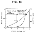
- Fig. 15 graphically illustrates characteristics of the intensity modulator element and the phase modulator element exhibited for applied bias voltages.
- operation characteristics of the modulators can easily be controlled or changed. More specifically, by applying a higher bias voltage to the intensity modulator element than the phase modulator element, absorption coefficient of the multiple quantum well is caused to change more significantly, whereby the degree of intensity modulation is increased.
- change in the intensity will take place more or less even in the phase modulator element.
- magnitude of such change can be suppressed to a sufficiently small value when compared with that of the intensity modulator element, to ensure desired operation.
- Fig. 16A shows an integrated structure of an optical modulator in which multiple quantum well structures having mutually different characteristics are adopted for a phase modulator element and an intensity modulator element, respectively.
- Figs. 16B and 16C are sectional views taken along lines a-a' and b-b' in Fig. 26A, respectively. With the structure shown in these figures, the intensity modulation characteristics and the phase modulation characteristic are isolated. The structure shown in Figs. 16A, 16B and 16C becomes advantageous over that shown in Fig. 23 because the modulator elements can be optimized independent of each other although the manufacturing process of the integrated optical modulator device shown in Figs. 16A, 16B and 16C is complicated.
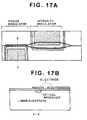
- Figs. 17A and 17B show an integrated optical transmitter structure realized by using a dielectric.
- the intensity modulator element is implemented in a Mach-Zehnder interferometer structure, while the phase modulator element is implemented in the form of a linear waveguide.
- the intensity modulator element can be implemented in other various structures inclusive of a directional coupler type intensity modulator and the like so far as the underlying operation principle is based on the electrooptical effect.
- similar device structure can be obtained when the electrooptical effect of semiconductor crystal such as GaAs, InP and the like is made use of.
- optical transmitter apparatus which can achieve the first and second objects of the invention simultaneously is also intended to be encompassed by the scope of the present invention.
- Fig. 18 shows a structure of an optical transmitter apparatus which includes the first embodiment of the invention.
- the optical transmitter apparatus 100 is composed of a light source 1 for signal transmission, an intensity modulator 2, phase modulators 3-a and 3-b, a transmit signal generator 4 and a spectrum spreading signal generator 5.
- a signal to be transmitted which is generated by a transmit signal generator 4 is supplied to the intensity modulator 2 and the phase modulator 3-a.
- An output signal of the spectrum spreading signal generator 5 is inputted to the phase modulator 3-b.
- the light beam emanated from the light source 1 is caused to pass through the intensity modulator 2 and the phase modulators 3-a and 3-b before being sent out from the optical transmitter apparatus 100.
- the light beam emanated from the light source 1 undergoes intensity modulation and feeble phase modulation or shift upon passing through the intensity modulator 2.
- the optical signal outputted from the intensity modulator 2 undergoes a phase modulation which can cancel out the feeble phase modulation or shift which the signal suffered upon passing through the intensity modulator 2.
- the output signal of the phase modulator 3-a is further subjected to a phase modulation by the phase modulator 3-b which is effective for spreading the spectrum of the optical signal.
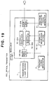
- Fig. 19 shows, by way of example a structure of an optical transmitter in which an optical intensity modulator and an optical phase modulator are integrated with each other. Owing to the integrated structure, optical loss at the coupling parts can be reduced. Besides, the number of optical elements which will otherwise be required can be decreased.
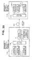
- Fig. 20 shows schematically a structure of a waveform division multiplex optical transmission system according to yet another embodiment of the invention.
- Each of optical transmitters 111-1, 111-2, ..., 111-n includes no optical phase modulator designed for spectrum spreading.
- each optical transmitter is composed of a light source, an intensity modulator and a signal generator for generating a signal to be optically transmitted.
- a plurality of optical signals generated by the individual intensity modulators and having mutually different wavelengths are optically synthesized by an optical coupler 116.
- the synthesized signal light beam undergoes en bloc a phase modulation in an optical phase modulator 3 in accordance with a signal generated by a spectrum spreading signal generator 5.
- the wavelength division multiplexed optical signal undergone the phase modulation is sent out onto an optical fiber 1001 from the wavelength multiplex division transmitter apparatus 110, and received by an optical wavelength demultiplexer 114 to be demultiplexed into the original wavelengths.
- Optical signals resulting from the optical demultiplexing are received by individual optical receivers 115-1, 115-2, ..., 115-n, respectively.
- the stimulated Brillouin scattering can be suppressed to a minimum because spectrum of the optical signal is spread.
- the optical transmitter apparatus 111 has been described as being composed of the light source, the intensity modulator and the transmit signal generator. It should however be understood that the optical transmitter apparatus may include a phase modulator for suppressing the chirping phenomenon. Parenthetically, the optical coupler 116 employed for synthesization of the optical signals may be replaced by an optical wavelength multiplexer.
- the stimulated Brillouin scattering can effectively be suppressed according to the teaching of the present invention that the optical signal undergone an optical phase modulation is transmitted.
- reception sensitivity can be protected against degradation due to the time jitter.
- optical intensity modulator and the optical phase modulator in an integrated structure, light energy loss at inter-element coupling or connecting portions can be reduced with the number of optical elements being decreased, to further advantages.
Landscapes
- Physics & Mathematics (AREA)
- Engineering & Computer Science (AREA)
- Nanotechnology (AREA)
- Chemical & Material Sciences (AREA)
- Optics & Photonics (AREA)
- Nonlinear Science (AREA)
- General Physics & Mathematics (AREA)
- Signal Processing (AREA)
- Life Sciences & Earth Sciences (AREA)
- Biophysics (AREA)
- Computer Networks & Wireless Communication (AREA)
- Crystallography & Structural Chemistry (AREA)
- Electromagnetism (AREA)
- Optical Communication System (AREA)
Applications Claiming Priority (3)
| Application Number | Priority Date | Filing Date | Title |
|---|---|---|---|
| JP85306/92 | 1992-04-07 | ||
| JP8530692 | 1992-04-07 | ||
| JP08530692A JP3223562B2 (ja) | 1992-04-07 | 1992-04-07 | 光送信装置、光伝送装置および光変調器 |
Publications (4)
| Publication Number | Publication Date |
|---|---|
| EP0565035A2 EP0565035A2 (en) | 1993-10-13 |
| EP0565035A3 EP0565035A3 (enExample) | 1994-12-28 |
| EP0565035B1 EP0565035B1 (en) | 2002-07-24 |
| EP0565035B9 true EP0565035B9 (en) | 2003-02-26 |
Family
ID=13854918
Family Applications (1)
| Application Number | Title | Priority Date | Filing Date |
|---|---|---|---|
| EP93105624A Expired - Lifetime EP0565035B9 (en) | 1992-04-07 | 1993-04-05 | Optical modulator optical transmitter apparatus and optical transmission system |
Country Status (4)
| Country | Link |
|---|---|
| US (1) | US5515196A (enExample) |
| EP (1) | EP0565035B9 (enExample) |
| JP (1) | JP3223562B2 (enExample) |
| DE (1) | DE69332131T2 (enExample) |
Families Citing this family (107)
| Publication number | Priority date | Publication date | Assignee | Title |
|---|---|---|---|---|
| US5394260A (en) * | 1992-02-03 | 1995-02-28 | Kokusai Denshin Denwa Kabushiki Kaisha | Optical pulse generator |
| JPH06261005A (ja) * | 1993-03-02 | 1994-09-16 | Matsushita Electric Ind Co Ltd | 光伝送装置 |
| US5373385A (en) * | 1993-11-12 | 1994-12-13 | At&T Corp. | Method and apparatus for reduction of optical communication system impairments |
| DE69531328T2 (de) * | 1994-09-12 | 2004-02-12 | Nippon Telegraph And Telephone Corp. | Intensitätsmoduliertes optisches Übertragungssystem |
| US5619364A (en) * | 1995-02-22 | 1997-04-08 | The United States Of America As Represented By The Secretary Of The Navy | Depolarized source for high power operation of an integrated optical modulator |
| US5566381A (en) * | 1995-03-02 | 1996-10-15 | Lucent Technologies Inc. | Multifrequency lightwave source using phase modulation for suppressing stimulated brillouin scattering in optical fibers |
| JP3304683B2 (ja) * | 1995-05-02 | 2002-07-22 | 富士通株式会社 | 無線装置 |
| JPH08316909A (ja) * | 1995-05-16 | 1996-11-29 | Toshiba Corp | 光伝送システム、光送信モジュール、及び光変調器の駆動方法 |
| JPH0946318A (ja) * | 1995-08-01 | 1997-02-14 | Fujitsu Ltd | 波長多重光伝送システム及び該伝送システムに用いる光送信装置 |
| JPH0961766A (ja) * | 1995-08-19 | 1997-03-07 | Nec Corp | 半導体光変調器 |
| US5828477A (en) * | 1995-11-16 | 1998-10-27 | Harmonic Lightwaves, Inc. | Multi-tone phase modulation for light wave communication system |
| JP3299101B2 (ja) * | 1995-12-15 | 2002-07-08 | 日本電気株式会社 | 波長多重光通信装置 |
| IT1279248B1 (it) | 1995-12-21 | 1997-12-09 | Pirelli Cavi S P A Ora Pirelli | Sistema di trasmissione di segnali ottici modulati e depolarizzati |
| US6310709B1 (en) * | 1995-12-29 | 2001-10-30 | Tyco Submarine Systems Ltd. | Synchronous polarization and phase modulation using a periodic waveform with complex harmonics for improved performance of optical transmission systems |
| JP3405046B2 (ja) * | 1996-02-22 | 2003-05-12 | Kddi株式会社 | レーザ光発生装置 |
| GB9604303D0 (en) * | 1996-02-29 | 1996-05-01 | Stc Submarine Systems Ltd | Chromatic pre-chip in NRZ transmitter |
| DE19617956A1 (de) * | 1996-05-04 | 1997-11-13 | Bosch Gmbh Robert | Optischer Sender |
| JP2955986B2 (ja) * | 1996-05-22 | 1999-10-04 | 日本電気株式会社 | 半導体光変調器及びその製造方法 |
| JPH09321709A (ja) * | 1996-05-29 | 1997-12-12 | Fujitsu Ltd | 光送信器 |
| JP3027944B2 (ja) * | 1996-08-16 | 2000-04-04 | 日本電気株式会社 | 光デュオバイナリ信号光の生成方法および光送信装置 |
| US5892607A (en) * | 1996-10-23 | 1999-04-06 | Scientific-Atlanta, Inc. | Suppression of stimulated brillouin scattering in optical transmission system |
| JP3512580B2 (ja) * | 1996-12-10 | 2004-03-29 | 日本電気株式会社 | 光時分割多重伝送用光送信装置と光受信装置及びこれらを備えた光時分割多重光伝送装置 |
| US20040161245A1 (en) * | 1996-12-20 | 2004-08-19 | Bergano Neal S. | Synchronous amplitude modulation for improved performance of optical transmission systems |
| US6556326B2 (en) * | 1996-12-20 | 2003-04-29 | Tyco Telecommunications (Us) Inc. | Synchronous amplitude modulation for improved performance of optical transmission systems |
| WO1998032247A1 (en) * | 1997-01-22 | 1998-07-23 | Advantest Corporation | Optical pulse transmission system, optical pulse transmitting method, and optical pulse detecting method |
| US5946119A (en) * | 1997-02-12 | 1999-08-31 | Tyco Submarine Systems Ltd. | Wavelength division multiplexed system employing optimal channel modulation |
| CA2197624C (en) * | 1997-02-14 | 2003-07-29 | Robert J. Davies | Hybrid single sideband optical modulator |
| CN1082753C (zh) * | 1997-03-05 | 2002-04-10 | 富士通株式会社 | 减小受激布里渊散射影响的传输波分复用信号方法和设备 |
| US6091864A (en) * | 1997-04-10 | 2000-07-18 | Ortel Corporation | Linear optical modulator for providing chirp-free optical signals |
| JP3094950B2 (ja) * | 1997-05-28 | 2000-10-03 | 日本電気株式会社 | 光送信装置及び光送信方法 |
| JPH1152313A (ja) * | 1997-08-08 | 1999-02-26 | Mitsubishi Electric Corp | 光変調装置 |
| US6388786B1 (en) * | 1997-08-15 | 2002-05-14 | Nec Corporation | Method for generating duobinary signal and optical transmitter using the same method |
| US6556327B1 (en) * | 1997-11-06 | 2003-04-29 | Matsushita Electric Industrial Co., Ltd. | Signal converter, optical transmitter and optical fiber transmission system |
| US6282003B1 (en) * | 1998-02-02 | 2001-08-28 | Uniphase Corporation | Method and apparatus for optimizing SBS performance in an optical communication system using at least two phase modulation tones |
| FR2781322B1 (fr) * | 1998-07-20 | 2000-09-08 | Alsthom Cge Alcatel | Dispositif d'emission de donnees optiques |
| US6320692B1 (en) | 1998-11-27 | 2001-11-20 | Pirelli Cavi E Sistemi S.P.A. | Biasing system for an optical modulator with double output |
| US6763151B1 (en) | 1999-07-02 | 2004-07-13 | Avanex Corporation | Electro-optic modulators with internal impedance matching |
| US6535315B1 (en) * | 2000-01-21 | 2003-03-18 | New Elite Technologies, Inc. | Optical fiber transmitter for simultaneously suppressing stimulated brillouin scattering and self/external-phase modulation-induced nolinear distortions in a long-distance broadband distribution system |
| FR2806559B1 (fr) * | 2000-03-20 | 2002-05-31 | Cit Alcatel | Regenerateur optique synchrone par modulation d'intensite et modulation de phase par effet kerr croise |
| JP2001296506A (ja) * | 2000-04-13 | 2001-10-26 | Nec Corp | Rz光送信器 |
| US6876818B1 (en) * | 2000-08-18 | 2005-04-05 | Futurewei Technologies, Inc. | Method and system for transmitting signals with spectrally enriched optical pulses |
| US6738105B1 (en) * | 2000-11-02 | 2004-05-18 | Intel Corporation | Coherent light despeckling |
| WO2002037622A2 (en) | 2000-11-06 | 2002-05-10 | Vitesse Semiconductor Corporation | Method of controlling the turn off characteristics of a vcsel diode |
| US7173551B2 (en) * | 2000-12-21 | 2007-02-06 | Quellan, Inc. | Increasing data throughput in optical fiber transmission systems |
| US6791694B2 (en) * | 2001-01-16 | 2004-09-14 | Santur Corporation | Tunable optical device using a scanning MEMS mirror |
| US20020131100A1 (en) * | 2001-03-16 | 2002-09-19 | Myers Michael H. | Method for photonic wavelength error detection |
| US20020131125A1 (en) * | 2001-03-16 | 2002-09-19 | Myers Michael H. | Replicated-spectrum photonic transceiving |
| US6407846B1 (en) | 2001-03-16 | 2002-06-18 | All Optical Networks, Inc. | Photonic wavelength shifting method |
| US7149256B2 (en) * | 2001-03-29 | 2006-12-12 | Quellan, Inc. | Multilevel pulse position modulation for efficient fiber optic communication |
| US7307569B2 (en) * | 2001-03-29 | 2007-12-11 | Quellan, Inc. | Increasing data throughput in optical fiber transmission systems |
| WO2002080317A1 (en) * | 2001-03-30 | 2002-10-10 | Santur Corporation | Alignment of an on chip modulator |
| WO2002079864A1 (en) * | 2001-03-30 | 2002-10-10 | Santur Corporation | Modulator alignment for laser |
| US6922278B2 (en) | 2001-03-30 | 2005-07-26 | Santur Corporation | Switched laser array modulation with integral electroabsorption modulator |
| US6816529B2 (en) | 2001-03-30 | 2004-11-09 | Santur Corporation | High speed modulation of arrayed lasers |
| CA2442922A1 (en) * | 2001-04-04 | 2002-10-17 | Quellan, Inc. | Method and system for decoding multilevel signals |
| US20030030873A1 (en) * | 2001-05-09 | 2003-02-13 | Quellan, Inc. | High-speed adjustable multilevel light modulation |
| US7483639B2 (en) * | 2001-05-10 | 2009-01-27 | Fujitsu Limited | Method and system for transmitting information in an optical communication system using distributed amplification |
| US7200344B1 (en) | 2001-05-10 | 2007-04-03 | Fujitsu Limited | Receiver and method for a multichannel optical communication system |
| US7035543B1 (en) | 2001-05-10 | 2006-04-25 | Fujitsu Limited | Method and system for demultiplexing non-intensity modulated wavelength division multiplexed (WDM) signals |
| US6941078B1 (en) * | 2001-05-10 | 2005-09-06 | Fujitsu Limited | Method and system for communicating a clock signal over an optical link |
| JP4698888B2 (ja) * | 2001-06-21 | 2011-06-08 | 三菱電機株式会社 | 光変調器、光変調器の実装基板および光変調器の駆動方法 |
| US7702245B1 (en) | 2001-08-15 | 2010-04-20 | Cisco Technology, Inc. | Spread spectrum in-band utility communication channel |
| US6865345B2 (en) * | 2001-08-28 | 2005-03-08 | Agilent Technologies, Inc. | Frequency translating devices and frequency translating measurement systems that utilize light-activated resistors |
| US7127182B2 (en) * | 2001-10-17 | 2006-10-24 | Broadband Royalty Corp. | Efficient optical transmission system |
| US6990296B2 (en) * | 2001-12-21 | 2006-01-24 | Fujitsu Limited | Optical phase modulation |
| AU2003211094A1 (en) * | 2002-02-15 | 2003-09-09 | Quellan, Inc. | Multi-level signal clock recovery technique |
| US6671077B2 (en) * | 2002-04-16 | 2003-12-30 | Lucent Technologies Inc. | Method and apparatus for generating return-to-zero modulated optical signals |
| AU2003223687A1 (en) * | 2002-04-23 | 2003-11-10 | Quellan, Inc. | Combined ask/dpsk modulation system |
| US7146109B2 (en) * | 2002-04-26 | 2006-12-05 | Lucent Technologies Inc. | Analog modulation of optical signals |
| US6819480B2 (en) * | 2002-05-02 | 2004-11-16 | Lucent Technologies Inc. | Method and apparatus for controlling the extinction ratio of transmitters |
| JP2004013681A (ja) * | 2002-06-10 | 2004-01-15 | Bosu & K Consulting Kk | 名刺情報管理システム |
| US20030235415A1 (en) * | 2002-06-21 | 2003-12-25 | Peters Frank H. | Optical communication devices and optical communication methods |
| US7035361B2 (en) | 2002-07-15 | 2006-04-25 | Quellan, Inc. | Adaptive noise filtering and equalization for optimal high speed multilevel signal decoding |
| US20040057734A1 (en) * | 2002-09-25 | 2004-03-25 | Lucent Technologies, Inc. | Method and system for reducing transmission penalties associated with ghost pulses |
| AU2003287628A1 (en) * | 2002-11-12 | 2004-06-03 | Quellan, Inc. | High-speed analog-to-digital conversion with improved robustness to timing uncertainty |
| US7146110B2 (en) | 2003-02-11 | 2006-12-05 | Optium Corporation | Optical transmitter with SBS suppression |
| US20040190661A1 (en) * | 2003-03-26 | 2004-09-30 | Quellan, Inc. | Method and system for equalizing communication signals |
| KR100547746B1 (ko) * | 2003-04-30 | 2006-01-31 | 삼성전자주식회사 | 듀오바이너리 광 전송장치 |
| US7269358B2 (en) * | 2003-08-01 | 2007-09-11 | Optium Corporation | Optical transmitter for increased effective modal bandwidth transmission |
| US20050025416A1 (en) * | 2003-08-01 | 2005-02-03 | Optium Corporation | Optical fiber transmission system with increased effective modal bandwidth transmission |
| WO2005018134A2 (en) * | 2003-08-07 | 2005-02-24 | Quellan, Inc. | Method and system for crosstalk cancellation |
| US7804760B2 (en) * | 2003-08-07 | 2010-09-28 | Quellan, Inc. | Method and system for signal emulation |
| US7215893B2 (en) * | 2003-08-28 | 2007-05-08 | The Boeing Company | RF photonics residual error correction |
| US7573928B1 (en) | 2003-09-05 | 2009-08-11 | Santur Corporation | Semiconductor distributed feedback (DFB) laser array with integrated attenuator |
| ATE488068T1 (de) | 2003-11-17 | 2010-11-15 | Quellan Inc | Verfahren und system zur löschung von antennenstörungen |
| US7616700B2 (en) * | 2003-12-22 | 2009-11-10 | Quellan, Inc. | Method and system for slicing a communication signal |
| EP1749357B1 (en) * | 2004-05-25 | 2009-04-22 | Azea Networks Limited | Method and apparatus for producing high extinction ratio data modulation formats |
| KR100617771B1 (ko) * | 2004-11-20 | 2006-08-28 | 삼성전자주식회사 | 영복귀-교호부호반전 광송신기 및 이를 이용한영복귀-교호부호반전 광신호의 생성 방법 |
| US7522883B2 (en) * | 2004-12-14 | 2009-04-21 | Quellan, Inc. | Method and system for reducing signal interference |
| US7725079B2 (en) | 2004-12-14 | 2010-05-25 | Quellan, Inc. | Method and system for automatic control in an interference cancellation device |
| GB2421863A (en) * | 2005-01-04 | 2006-07-05 | Salah A Al-Chalabi | Using an interferometer to impose a spread spectrum code and data modulation in an optical communication system |
| US7761011B2 (en) * | 2005-02-23 | 2010-07-20 | Kg Technology Associates, Inc. | Optical fiber communication link |
| US7848661B2 (en) * | 2005-03-15 | 2010-12-07 | Emcore Corporation | Directly modulated laser optical transmission system with phase modulation |
| KR101372361B1 (ko) | 2006-04-26 | 2014-03-12 | 인터실 아메리카스 엘엘씨 | 통신 채널로부터 복사성 방출을 감소시키기 위한 방법 및 시스템 |
| JP2008211439A (ja) | 2007-02-26 | 2008-09-11 | Yokogawa Electric Corp | 光送信器 |
| TW200840362A (en) * | 2007-03-28 | 2008-10-01 | Emcore Corp | Externally modulated laser optical transmission system with feed forward noise cancellation |
| US8948273B2 (en) * | 2007-09-17 | 2015-02-03 | J. Craig Oxford | Method and apparatus for wired signal transmission |
| US8208817B2 (en) * | 2009-03-20 | 2012-06-26 | Alcatel Lucent | High-speed optical modulation using a quantum-well modulator |
| WO2011133222A2 (en) * | 2010-04-21 | 2011-10-27 | Aurora Networks, Inc. | Chirp compensation and sbs suppression using a multi-section laser |
| CN103905125B (zh) * | 2014-04-25 | 2016-09-14 | 中国电子科技集团公司第四十四研究所 | 模拟微波光链路幅相调控装置 |
| US20180269645A1 (en) * | 2016-02-29 | 2018-09-20 | The Johns Hopkins University | High energy fiber laser amplifier with reduced optical linewidth |
| US10811837B2 (en) * | 2017-12-18 | 2020-10-20 | Northrop Grumman Systems Corporation | AM/FM seed for nonlinear spectrally compressed fiber amplifier |
| US11411366B2 (en) * | 2019-01-15 | 2022-08-09 | Northrop Grumman Systems Corporation | Combined laser architecture using wavelength multiplexed seed source |
| CN114448518B (zh) * | 2020-11-04 | 2024-01-30 | 西安电子科技大学 | 一种低复杂度相干检测光载射频链路的方法 |
| JP2024058965A (ja) * | 2022-10-17 | 2024-04-30 | 日本電気株式会社 | 光通信システムにおける送信機、ネスト型変調器の制御方法およびプログラム |
| US12298648B2 (en) * | 2022-12-21 | 2025-05-13 | Luminous Computing, Inc. | Optical modulator with twisted electrodes |
| EP4531306A1 (en) * | 2023-09-27 | 2025-04-02 | NKT Photonics A/S | Optical ground terminal optical transmission system and an optical ground terminal |
Family Cites Families (12)
| Publication number | Priority date | Publication date | Assignee | Title |
|---|---|---|---|---|
| US3875400A (en) * | 1971-04-06 | 1975-04-01 | Pao Yoh Han | Intensity modulated optical carrier communication system |
| JPS6313017A (ja) * | 1986-07-03 | 1988-01-20 | Nec Corp | 光振幅位相変調器 |
| US4754452A (en) * | 1986-09-11 | 1988-06-28 | American Telephone And Telegraph Company, At&T Bell Laboratories | Optical local area network using a common optical carrier with separate user angle modulation |
| JPS645127A (en) * | 1987-06-29 | 1989-01-10 | Nec Corp | Optical transmitter |
| WO1989008356A1 (fr) * | 1988-03-04 | 1989-09-08 | Fujitsu Limited | Procede et dispositif de modulation d'un laser a semi-conducteur |
| JP2658387B2 (ja) * | 1989-04-28 | 1997-09-30 | 日本電気株式会社 | 光変調器とその駆動方法および光変調器駆動装置 |
| US5031235A (en) * | 1989-10-27 | 1991-07-09 | Hoechst Celanese Corp. | Cable system incorporating highly linear optical modulator |
| DE69017848T2 (de) * | 1989-11-30 | 1995-07-06 | Nippon Electric Co | Optische Übertragungsvorrichtung. |
| JP2917333B2 (ja) * | 1989-11-30 | 1999-07-12 | 日本電気株式会社 | 光送信方法及び光送信装置 |
| JP2946630B2 (ja) * | 1990-05-08 | 1999-09-06 | 富士通株式会社 | 光変調器 |
| US5301058A (en) * | 1990-12-31 | 1994-04-05 | Gte Laboratories Incorporated | Single sideband optical modulator for lightwave systems |
| JPH0539177A (ja) * | 1991-08-02 | 1993-02-19 | Fujitec Co Ltd | エレベータホール等の混雑度検出装置 |
-
1992
- 1992-04-07 JP JP08530692A patent/JP3223562B2/ja not_active Expired - Lifetime
-
1993
- 1993-04-02 US US08/042,380 patent/US5515196A/en not_active Expired - Lifetime
- 1993-04-05 DE DE69332131T patent/DE69332131T2/de not_active Expired - Fee Related
- 1993-04-05 EP EP93105624A patent/EP0565035B9/en not_active Expired - Lifetime
Also Published As
| Publication number | Publication date |
|---|---|
| JP3223562B2 (ja) | 2001-10-29 |
| US5515196A (en) | 1996-05-07 |
| EP0565035A2 (en) | 1993-10-13 |
| EP0565035B1 (en) | 2002-07-24 |
| JPH05289125A (ja) | 1993-11-05 |
| DE69332131D1 (de) | 2002-08-29 |
| DE69332131T2 (de) | 2003-03-27 |
| EP0565035A3 (enExample) | 1994-12-28 |
Similar Documents
| Publication | Publication Date | Title |
|---|---|---|
| EP0565035B9 (en) | Optical modulator optical transmitter apparatus and optical transmission system | |
| EP1004920B1 (en) | Optical modulator and method of controlling the same | |
| EP0950167B1 (en) | Variable chirp optical modulator using single modulation source | |
| US5926297A (en) | Optical modulating device and optical modulating method | |
| JP3028906B2 (ja) | ソリトン光通信システム及びその光送信装置と光受信装置 | |
| CA2124124C (en) | Ultra-high capacity non-soliton optical transmission using optical phaseconjugation | |
| US5699179A (en) | Cancellation of distortion components in a fiber optic link with feed-forward linearization | |
| JPH09167998A (ja) | 波長多重光通信装置 | |
| NZ294023A (en) | Non-linear combining of wavelength division multiplexed optical signals with clock signal then applying wavelength dependent delay | |
| JP2002023121A (ja) | 光送信装置及びそれを有する光ファイバ伝送システム | |
| EP1171968B1 (en) | Device and method for compensating polarization mode dispersion in an optical communication system | |
| Prabu et al. | Analysis of optical modulators for radio over free space optical communication systems and radio over fiber systems | |
| US20040070832A1 (en) | Electro-optic gating arrangement with improved duty cycle | |
| US7412173B2 (en) | Apparatus for generating optical carrier suppressed return-to-zero | |
| US20020057478A1 (en) | System and transmitter for transmitting optical data | |
| US7050722B2 (en) | Synchronous optical regenerator using intensity modulation and phase modulation by the crossed kerr effect | |
| US20020109888A1 (en) | Modulation scheme and transmission system for NRZ signals with left and right side filtering | |
| JP3322653B2 (ja) | ダークソリトン光通信システムに用いる光受信装置 | |
| Abejide et al. | Direct and external hybrid modulation approaches for access networks | |
| US20050141072A1 (en) | Electroabsorption modulator with two sections | |
| CA2272376A1 (en) | Variable chirp optical modulator using single modulation source | |
| HK1005284B (en) | Cancellation of distortion components in a fiber optic link with feed-forward linearization |
Legal Events
| Date | Code | Title | Description |
|---|---|---|---|
| PUAI | Public reference made under article 153(3) epc to a published international application that has entered the european phase |
Free format text: ORIGINAL CODE: 0009012 |
|
| AK | Designated contracting states |
Kind code of ref document: A2 Designated state(s): DE FR GB |
|
| PUAL | Search report despatched |
Free format text: ORIGINAL CODE: 0009013 |
|
| AK | Designated contracting states |
Kind code of ref document: A3 Designated state(s): DE FR GB |
|
| 17P | Request for examination filed |
Effective date: 19950530 |
|
| 17Q | First examination report despatched |
Effective date: 19990519 |
|
| GRAG | Despatch of communication of intention to grant |
Free format text: ORIGINAL CODE: EPIDOS AGRA |
|
| GRAG | Despatch of communication of intention to grant |
Free format text: ORIGINAL CODE: EPIDOS AGRA |
|
| GRAH | Despatch of communication of intention to grant a patent |
Free format text: ORIGINAL CODE: EPIDOS IGRA |
|
| GRAH | Despatch of communication of intention to grant a patent |
Free format text: ORIGINAL CODE: EPIDOS IGRA |
|
| GRAA | (expected) grant |
Free format text: ORIGINAL CODE: 0009210 |
|
| AK | Designated contracting states |
Kind code of ref document: B1 Designated state(s): DE FR GB |
|
| REG | Reference to a national code |
Ref country code: GB Ref legal event code: FG4D |
|
| REF | Corresponds to: |
Ref document number: 69332131 Country of ref document: DE Date of ref document: 20020829 |
|
| ET | Fr: translation filed | ||
| PLBE | No opposition filed within time limit |
Free format text: ORIGINAL CODE: 0009261 |
|
| 26N | No opposition filed |
Effective date: 20030425 |
|
| PGFP | Annual fee paid to national office [announced via postgrant information from national office to epo] |
Ref country code: GB Payment date: 20070326 Year of fee payment: 15 |
|
| PGFP | Annual fee paid to national office [announced via postgrant information from national office to epo] |
Ref country code: DE Payment date: 20070606 Year of fee payment: 15 |
|
| PGFP | Annual fee paid to national office [announced via postgrant information from national office to epo] |
Ref country code: FR Payment date: 20070320 Year of fee payment: 15 |
|
| GBPC | Gb: european patent ceased through non-payment of renewal fee |
Effective date: 20080405 |
|
| PG25 | Lapsed in a contracting state [announced via postgrant information from national office to epo] |
Ref country code: DE Free format text: LAPSE BECAUSE OF NON-PAYMENT OF DUE FEES Effective date: 20081101 |
|
| REG | Reference to a national code |
Ref country code: FR Ref legal event code: ST Effective date: 20081231 |
|
| PG25 | Lapsed in a contracting state [announced via postgrant information from national office to epo] |
Ref country code: FR Free format text: LAPSE BECAUSE OF NON-PAYMENT OF DUE FEES Effective date: 20080430 |
|
| PG25 | Lapsed in a contracting state [announced via postgrant information from national office to epo] |
Ref country code: GB Free format text: LAPSE BECAUSE OF NON-PAYMENT OF DUE FEES Effective date: 20080405 |