EP0554061A1 - Flüssigkristallanzeige - Google Patents
Flüssigkristallanzeige Download PDFInfo
- Publication number
- EP0554061A1 EP0554061A1 EP93300570A EP93300570A EP0554061A1 EP 0554061 A1 EP0554061 A1 EP 0554061A1 EP 93300570 A EP93300570 A EP 93300570A EP 93300570 A EP93300570 A EP 93300570A EP 0554061 A1 EP0554061 A1 EP 0554061A1
- Authority
- EP
- European Patent Office
- Prior art keywords
- liquid crystal
- crystal display
- conductive layer
- pixel electrode
- pixel
- Prior art date
- Legal status (The legal status is an assumption and is not a legal conclusion. Google has not performed a legal analysis and makes no representation as to the accuracy of the status listed.)
- Granted
Links
Images


Classifications
-
- G—PHYSICS
- G02—OPTICS
- G02F—OPTICAL DEVICES OR ARRANGEMENTS FOR THE CONTROL OF LIGHT BY MODIFICATION OF THE OPTICAL PROPERTIES OF THE MEDIA OF THE ELEMENTS INVOLVED THEREIN; NON-LINEAR OPTICS; FREQUENCY-CHANGING OF LIGHT; OPTICAL LOGIC ELEMENTS; OPTICAL ANALOGUE/DIGITAL CONVERTERS
- G02F1/00—Devices or arrangements for the control of the intensity, colour, phase, polarisation or direction of light arriving from an independent light source, e.g. switching, gating or modulating; Non-linear optics
- G02F1/01—Devices or arrangements for the control of the intensity, colour, phase, polarisation or direction of light arriving from an independent light source, e.g. switching, gating or modulating; Non-linear optics for the control of the intensity, phase, polarisation or colour
- G02F1/13—Devices or arrangements for the control of the intensity, colour, phase, polarisation or direction of light arriving from an independent light source, e.g. switching, gating or modulating; Non-linear optics for the control of the intensity, phase, polarisation or colour based on liquid crystals, e.g. single liquid crystal display cells
- G02F1/133—Constructional arrangements; Operation of liquid crystal cells; Circuit arrangements
- G02F1/136—Liquid crystal cells structurally associated with a semi-conducting layer or substrate, e.g. cells forming part of an integrated circuit
- G02F1/1362—Active matrix addressed cells
- G02F1/136213—Storage capacitors associated with the pixel electrode
-
- G—PHYSICS
- G02—OPTICS
- G02F—OPTICAL DEVICES OR ARRANGEMENTS FOR THE CONTROL OF LIGHT BY MODIFICATION OF THE OPTICAL PROPERTIES OF THE MEDIA OF THE ELEMENTS INVOLVED THEREIN; NON-LINEAR OPTICS; FREQUENCY-CHANGING OF LIGHT; OPTICAL LOGIC ELEMENTS; OPTICAL ANALOGUE/DIGITAL CONVERTERS
- G02F1/00—Devices or arrangements for the control of the intensity, colour, phase, polarisation or direction of light arriving from an independent light source, e.g. switching, gating or modulating; Non-linear optics
- G02F1/01—Devices or arrangements for the control of the intensity, colour, phase, polarisation or direction of light arriving from an independent light source, e.g. switching, gating or modulating; Non-linear optics for the control of the intensity, phase, polarisation or colour
- G02F1/13—Devices or arrangements for the control of the intensity, colour, phase, polarisation or direction of light arriving from an independent light source, e.g. switching, gating or modulating; Non-linear optics for the control of the intensity, phase, polarisation or colour based on liquid crystals, e.g. single liquid crystal display cells
- G02F1/133—Constructional arrangements; Operation of liquid crystal cells; Circuit arrangements
- G02F1/1333—Constructional arrangements; Manufacturing methods
- G02F1/1335—Structural association of cells with optical devices, e.g. polarisers or reflectors
- G02F1/133509—Filters, e.g. light shielding masks
- G02F1/133512—Light shielding layers, e.g. black matrix
-
- G—PHYSICS
- G02—OPTICS
- G02F—OPTICAL DEVICES OR ARRANGEMENTS FOR THE CONTROL OF LIGHT BY MODIFICATION OF THE OPTICAL PROPERTIES OF THE MEDIA OF THE ELEMENTS INVOLVED THEREIN; NON-LINEAR OPTICS; FREQUENCY-CHANGING OF LIGHT; OPTICAL LOGIC ELEMENTS; OPTICAL ANALOGUE/DIGITAL CONVERTERS
- G02F1/00—Devices or arrangements for the control of the intensity, colour, phase, polarisation or direction of light arriving from an independent light source, e.g. switching, gating or modulating; Non-linear optics
- G02F1/01—Devices or arrangements for the control of the intensity, colour, phase, polarisation or direction of light arriving from an independent light source, e.g. switching, gating or modulating; Non-linear optics for the control of the intensity, phase, polarisation or colour
- G02F1/13—Devices or arrangements for the control of the intensity, colour, phase, polarisation or direction of light arriving from an independent light source, e.g. switching, gating or modulating; Non-linear optics for the control of the intensity, phase, polarisation or colour based on liquid crystals, e.g. single liquid crystal display cells
- G02F1/133—Constructional arrangements; Operation of liquid crystal cells; Circuit arrangements
- G02F1/136—Liquid crystal cells structurally associated with a semi-conducting layer or substrate, e.g. cells forming part of an integrated circuit
- G02F1/1362—Active matrix addressed cells
- G02F1/136218—Shield electrodes
-
- G—PHYSICS
- G02—OPTICS
- G02F—OPTICAL DEVICES OR ARRANGEMENTS FOR THE CONTROL OF LIGHT BY MODIFICATION OF THE OPTICAL PROPERTIES OF THE MEDIA OF THE ELEMENTS INVOLVED THEREIN; NON-LINEAR OPTICS; FREQUENCY-CHANGING OF LIGHT; OPTICAL LOGIC ELEMENTS; OPTICAL ANALOGUE/DIGITAL CONVERTERS
- G02F1/00—Devices or arrangements for the control of the intensity, colour, phase, polarisation or direction of light arriving from an independent light source, e.g. switching, gating or modulating; Non-linear optics
- G02F1/01—Devices or arrangements for the control of the intensity, colour, phase, polarisation or direction of light arriving from an independent light source, e.g. switching, gating or modulating; Non-linear optics for the control of the intensity, phase, polarisation or colour
- G02F1/13—Devices or arrangements for the control of the intensity, colour, phase, polarisation or direction of light arriving from an independent light source, e.g. switching, gating or modulating; Non-linear optics for the control of the intensity, phase, polarisation or colour based on liquid crystals, e.g. single liquid crystal display cells
- G02F1/133—Constructional arrangements; Operation of liquid crystal cells; Circuit arrangements
- G02F1/136—Liquid crystal cells structurally associated with a semi-conducting layer or substrate, e.g. cells forming part of an integrated circuit
- G02F1/1362—Active matrix addressed cells
- G02F1/136227—Through-hole connection of the pixel electrode to the active element through an insulation layer
Definitions
- the present invention relates to a liquid crystal display (LCD). Particularly, the present invention relates to a liquid crystal display in which individual pixel electrodes are provided for each of pixels.
- LCD liquid crystal display
- a liquid crystal display of a matrix type used in an image information processing apparatus such as a video camera recorder or a television is driven by a drive system which is either a simple matrix drive system or an active matrix (AM) drive system.
- a drive system which is either a simple matrix drive system or an active matrix (AM) drive system.
- a switching active element is provided for each pixel so as to prevent a signal from being input to a pixel electrode during a non-select period in order to prevent a cross-talk phenomenon which might occur between scanning lines with a simple matrix drive system.
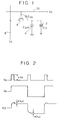
- Fig. 1 shows a circuit equivalent to a circuit corresponding to one pixel of a liquid crystal display using an active matrix drive system.
- the circuit includes a liquid crystal layer 2 having a capacitance C LC , a storage capacitance element 4 provided in parallel with the capacitance C LC and having a capacitance C ADD , a metal-oxide semiconductor (MOS) transistor 6 serving as a switching active element, a signal line 8 for supplying driving voltage V S to the liquid crystal layer 2, and a gate line 10 for controlling a gate voltage V G of the switching transistor 6.
- MOS metal-oxide semiconductor
- a parasitic capacitance C GD exists between the gate and the drain of the switching transistor 6.
- the parasitic capacitance C GD causes a reduction in a voltage V LC applied to the liquid crystal, as shown in Fig. 2. That is, a voltage swing occurs.
- the storage capacitance C ADD be as great as possible so that the swing ⁇ V LC can be minimized.
- the storage capacitance element 4 is formed by using an opaque material, such as that used in agate line or an active layer of a switching transistor, so as to achieve a great storage capacitance C ADD , the proportion of an opaque portion relatively increases, causing a corresponding reduction in the open area ratio.
- the use of a great storage capacitance C ADD is also disadvantageous in that it is necessary to increase the charging and discharging ability of the switching transistor 6, thereby requiring the use of a large-size transistor.
- ITO-ITO indium-tin oxide
- capacitances other than the above C GD that can add to the parasitic capacitance; these include a capacitance C GP between the gate line 10 and the pixel electrode 16, and a capacitance C SP between the signal line 8 and the pixel electrode 16. These capacitances C GP and C SP can cause reductions in the voltage V LC applied to the liquid crystal as does the capacitance C GD .
- the capacitance C GP causes a change corresponding to a change in the potential of the gate line 10
- the capacitance C SP causes a change corresponding to a change in the potential of the signal line 8.
- a primary object of the present invention is to decrease the parasitic capacitance between, for instance, a gate line and a pixel electrode and a signal line and a pixel electrode, while increasing the open area ratio, and thus to enable displays having satisfactorily high levels of definition and gradation.
- Another object of the present invention is to provide a liquid crystal display and an image information processing apparatus including such a liquid crystal display, the liquid crystal display having a plurality of sets of matrix wiring elements, a plurality of active elements and a liquid crystal layer, the liquid crystal display including a conductive layer selectively provided, for being maintained at a predetermined potential, around each of pixel electrodes individually provided for each of pixels.
- the selective formation of the conductive layer makes it possible to achieve the above object while reducing the risk of unwanted parasitic capacitance and leakage current being generated.
- a conductive layer used in the present invention is selectively provided around each of a plurality of pixel electrodes.
- the conductive layer is maintained at a predetermined potential so that the pixel electrode is prevented from being adversely effected by floating capacitance between the pixel electrode and matrix wiring elements or capacitance between lines.
- such a conductive layer may be formed in either the same process as or a different process from the corresponding pixel electrode. Further, the conductive layer may be positioned below a peripheral portion of the pixel electrode or beside the pixel electrode or both.
- the conductive layer need not be maintained at a fixed potential, and may be maintained at, for example, a binary potential, as is a gate selecting line among the matrix wiring elements.
- the conductive layer is preferably provided along at least three of the four sides of the pixel-electrode configuration. Specifically, the conductive layer is preferably provided at least between the pixel electrode and a gate selecting line corresponding to the same pixel as the pixel electrode, between the pixel electrode and a signal line corresponding to the same pixel as the pixel electrode, and between the pixel electrode and another signal line corresponding to an adjacent pixel.
- Figs. 3(a) and 3(b) show an arrangement corresponding to one of a plurality of pixels of an active matrix liquid crystal display (AM-LCD) according to a first embodiment of the present invention, Figs. 3(a) and 3(b) respectively showing a planar structure and a sectional structure of the arrangement.
- AM-LCD active matrix liquid crystal display
- the arrangement includes a MOS transistor 6 serving as a switching active element, a signal line 8, and a gate line 10 for controlling the gate voltage of the switching transistor 6, the gate line 10 serving as a gate selecting line among matrix wiring elements.
- the arrangement also includes a portion of a transparent substrate 12, a transparent pixel-electrode 16, and transparent insulating films 20, 22 and 24.
- a common potential wire 26 for storage capacitance is formed in a substantially ring-shaped configuration around the periphery of the pixel electrode 16.
- the storage capacitance wire 26 is connected to a reference voltage supply V Ref by a wire portion 26a so as to be maintained at a predetermined potential during a drive period of the corresponding pixel.
- the storage capacitance wire 26 is maintained at the same potential as a common electrode which is maintained at a common potential with respect to all the pixels and which is provided on another substrate disposed in opposition to the pixel electrodes.
- the storage capacitance wire 26 has a portion positioned between the pixel electrode 16, on one hand, and the signal line 8 or another signal line 8', on the other, so that a capacitance. is formed between the wire 26 and the signal lines 8 and 8'.
- the parasitic capacitance C SP between the pixel electrode 16 and the signal line 8 or 8' is greatly decreased.
- the storage capacitance wire 26 has another portion positioned between the pixel electrode 16 and the gate line 10, so that a capacitance is formed between the wire 26 and the gate line 10, resulting in the parasitic capacitance C GP between the pixel electrode 16 and the gate line 10 being greatly decreased.
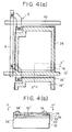
- Figs. 4(a) and 4(b) show an arrangement corresponding to one of a plurality of pixels of another AM-LCD according to a second embodiment of the present invention, Figs. 4(a) and 4(b) respectively showing a planar structure and a sectional structure of the arrangement.
- the construction of the second embodiment is basically the same as that of the first embodiment, and is distinguished therefrom in that a storage capacitance wire 26 is connected to a gate line 10' belonging to another pixel row, and that an outer edge portion of the wire 26 outwardly projects slightly beyond the outer edge of the corresponding pixel electrode 16.
- the gate line 10' is maintained at a certain potential during a time period during which the illustrated pixel row is driven by the gate line 10.
- the second embodiment is also able to greatly decrease the parasitic capacitance C SP between the pixel electrode 16 and the signal line 8 as well as the parasitic capacitance C GP between the pixel electrode 16 and the gate line 10 for driving the corresponding pixel.
- the second embodiment provides effects similar to those of the first embodiment. According to the second embodiment, since the storage capacitance wire and the gate line can be simultaneously formed using the same material, the layer formation processing is facilitated.
- Figs. 5(a) and 5(b) show an arrangement corresponding to one of a plurality of pixels of still another AM-LCD according to a third embodiment of the present invention, Figs. 5(a) and 5(b) respectively showing a planar structure and a sectional structure of the arrangement.
- the construction of the third embodiment is basically the same as that of the second embodiment, and is distinguished therefrom in the following points:
- Embodiment 3 while a common potential wire 26 for storage capacitance is formed as in Embodiment 2, a drain region 28 of a switching transistor 6 extends along a part of the outer periphery of the corresponding pixel electrode 16.
- This construction provides the following effects in addition to effects similar to those provided by Embodiments 1 and 2: Since an additional storage capacitance is formed between the wire 26 and the drain region 28, it possible to achieve a sufficient capacitance value even if the width of the wire 26 is reduced, thereby enabling a further increase in the open area ratio.
- a common potential wire for storage capacitance is provided around the outer periphery of the corresponding pixel electrode.
- a swing of the liquid-crystal application voltage V LC which can be caused by voltage variations in the signal line or the gate line, is reduced, thereby improving image quality.
- V LC liquid-crystal application voltage
- This makes it possible to decrease the storage capacitance value while the image quality is maintained, and hence, to accordingly reduce the size of the switching transistor as well as the width of the storage capacitance wire.
- the effectiveness of the above embodiments of the present invention increase as the pixel size decreases.
- Figs. 6(a) and 6(b) show an arrangement corresponding to one of a plurality of pixels of a further AM-LCD according to a fourth embodiment of the present invention, Figs. 6(a) and 6(b) respectively showing a planar structure and a sectional structure of the arrangement.
- the arrangement includes a gate line 10 for a pixel switch (a portion of the gate line 10 branching to form a gate electrode), a signal line 8 for writing an image signal in the corresponding pixel, and a MOS transistor 6 having semiconductor regions constituting a drain region, a channel region and a source region.
- the arrangement also includes a pixel electrode 16 for driving a portion of a liquid crystal layer 57, and a shielding wire 26 arranged between the pixel electrode 16, on one hand, and the gate line 10 or the signal line 8, on the other.
- Reference numeral 10' denotes another gate line corresponding to another pixel.
- Reference numerals 31, 32, 33, 34 and 35 denote transparent insulating layers.
- the shielding wire 26 When forming the shielding wire 26, it is cnmposed of two or three sublayers at different levels.
- the shielding wire 26 has an upper sublayer 26a and a lower sublayer 26c.
- the upper sublayer 26a is formed after a contact hole is formed in the insulating layers 33 and 34 at a position above the lower sublayer 26c so that the upper and lower sublayers 26a and 26c are interconnected with each other through a contact hole portion 26b in the contact hole.
- another sublayer to be disposed in a contact hole is formed in a step different from the step of forming an upper sublayer 26a.
- the lower sublayer 26c, the contact hole portion 26b and the upper sublayer 26a are formed in such a manner as to surround the entire periphery of the pixel electrode 16 except for a portion of the pixel electrode 16 at which the pixel switch is formed.
- the contact hole opens in a linear form around the mated periphery of the pixel electrode 16.
- the lower sublayer 26c may be formed by patterning a conductive layer at the same level as a conductive layer (such as an aluminum wire) for forming the signal line 8.
- the liquid crystal display shown in Figs. 6 (a) and 6(b) is driven in the following manner:
- a potential corresponding to an image signal is applied to the signal line 8
- a potential for conducting the pixel switch is applied to the gate line 10
- the pixel electrode 16 is brought to a predetermined potential.
- such an operation of writing into pixel electrode is performed simultaneously with respect to all pixel electrodes in one row.
- the gate lines of cells in one row are commonly connected.
- another writing operation with respect to another (adjacent) row is performed by using the same signal line.
- the signal lines belonging to one column are commonly connected.
- a shielding region, or the wire 26 is disposed around a pixel electrode and is maintained at a certain potential. Therefore, the influence of variations in the potential of the gate line and the signal line can be greatly reduced, thereby making it possible to improve image quality.
- the contact hole in the form of a linear opening and the contact hole portion 26b, as well as the lower and upper sublayers 26c and 26a, are formed in such a manner as to surround a certain peripheral portion of the corresponding pixel electrode 16, the contact hole and the contact hole portion 26b need not extend along the whole of that peripheral portion.
- active elements 6 are formed on a substrate 12 having an insulating surface by forming thereon a plurality of islands of a single-crystal semiconductor.
- a gate insulating film 31 and a plurality of gate electrodes 10, 10' are formed.
- another insulating layer 32 is formed.
- a conductor is deposited and patterned, thereby forming signal lines 8 and lower sublayers 26c simultaneously.
- a third insulating layer 33 is formed. Then, another contact hole, through which each active element 6 is to contact a pixel electrode 16, is formed in the insulating layers 31, 32 and 33.
- pixel electrodes 16 are formed by depositing and patterning a transparent conductor.
- the insulating layer 33 is subjected to a planarization process using a method such as a phosphosilicate glass re-flow method or a method comprising a combination of a spin-on glass step and an etch-back step, thereby planarizing the surface of the insulating layer 33.
- the pixel electrodes 16 thus formed are covered with a fourth insulating layer 34.
- a contact hole, through which each lower sublayer 26c is to contact an upper sublayer 26a, is formed in the insulating layers 33 and 34.
- upper sublayers 26a are formed by depositing and patterning a conductor.
- a protecting layer 35 is formed, thereby completing a structure including one of a pair of substrates, between which a liquid crystal layer 57 will be held.
- a structure including another substrate 56 and a common electrode thereon is prepared, and fixed in position with a prescribed gap defined between the substrate structures. Then, a liquid crystal 57 is charged in the gap. Peripheral portions of the substrate structures are sealed, thereby completing an AM-LCD such as that described above.
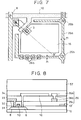
- Fig. 7 is a fragmentary plan view schematically showing an arrangement corresponding to one of a plurality of pixels of a still further AM-LCD according to a fifth embodiment of the present invention.
- the construction of the fifth embodiment is basically the same as that of the fourth embodiment, and is distinguished therefrom in the following points:
- contact hole portions 26b are formed only at limited locations of a shielding wire 26; and those portions of an upper sublayer 26a and a lower sublayer 26c where no contact hole is formed have a decreased width m .
- This construction makes it possible to increase the pixel area, and thus, to increase the open area ratio.
- Fig. 8 is a sectional view, which can be taken along line B-B shown in Fig. 7, schematically showing an arrangement corresponding to one of a plurality of pixels of a still further AM-LCD according to a sixth embodiment of the present invention.
- the construction of the sixth embodiment is basically the same as that of the fourth and fifth embodiments, and is distinguished therefrom in the following points:
- an upper sublayer 26a of a shielding wire 26 is formed by patterning the same conductor layer that is to form a pixel electrode 16; and a lower sublayer 26c is formed by patterning the same conductor layer that is to form a signal line 8.
- a shielding region formed in the above embodiments surrounds a greater part of the periphery of the corresponding pixel electrode. Therefore, if the shield region is formed by using a light-shielding electrically-conductive material, it is possible to prevent penetration of light into gaps between pixels (i.e., cross-talk of light) as well.
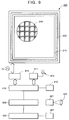
- Fig. 9 schematically shows an image information processing apparatus incorporating a liquid crystal display (LCD) according to the present invention.
- LCD liquid crystal display
- the apparatus includes a LCD 300 having a display section 310 on the center thereof.
- a display section 310 on the center thereof.
- an active matrix portion 204 on a substrate is depicted on an enlarged scale.
- Peripheral circuitry including a shift register is disposed on a peripheral area 203 around the display section 310.
- the peripheral circuitry includes horizontal drive circuits disposed above and below the display section 310, and drive circuits disposed on the left and right of the display section 310, as viewed in the drawing.
- the horizontal drive circuits are connected to signal lines to supply an image signal thereto.
- the drive circuits generates a line selection signal, and are connected to gate lines.
- These drive circuits are also connected to a drive control circuit 410 mounted on another substrate, so as to be controlled thereby.
- a lighting control circuit 411 includes a light source 412 and an inverter for controlling the lighting of the light source 412.
- the drive control circuit 410 and the lighting control circuit 411 are connected to a central control circuit 414.
- the image information processing apparatus further includes an optical system 422 including a lens through which image information is input, an image sensor 421 including a photo-electric conversion element, and a drive circuit 420 for driving the image sensor 421.
- the apparatus includes a recording control circuit 430 including a recording head 431 so that image information obtained by the image sensor 421 and/or image information displayed on the display section 310 can be recorded on a recording medium.
- a shielding region is provided between a pixel electrode and matrix wiring elements in such a manner as to surround the pixel electrode. Therefore, it is possible to greatly reduce adverse influence of potential variations in matrix wiring elements such as gate lines and signal lines.
Applications Claiming Priority (4)
| Application Number | Priority Date | Filing Date | Title |
|---|---|---|---|
| JP38463/92 | 1992-01-30 | ||
| JP3846392 | 1992-01-30 | ||
| JP41948/92 | 1992-01-31 | ||
| JP4194892 | 1992-01-31 |
Publications (2)
| Publication Number | Publication Date |
|---|---|
| EP0554061A1 true EP0554061A1 (de) | 1993-08-04 |
| EP0554061B1 EP0554061B1 (de) | 1998-05-13 |
Family
ID=26377728
Family Applications (1)
| Application Number | Title | Priority Date | Filing Date |
|---|---|---|---|
| EP93300570A Expired - Lifetime EP0554061B1 (de) | 1992-01-30 | 1993-01-27 | Flüssigkristallanzeige |
Country Status (3)
| Country | Link |
|---|---|
| US (1) | US5666180A (de) |
| EP (1) | EP0554061B1 (de) |
| DE (1) | DE69318434T2 (de) |
Cited By (5)
| Publication number | Priority date | Publication date | Assignee | Title |
|---|---|---|---|---|
| EP0592063A2 (de) * | 1992-09-14 | 1994-04-13 | Kabushiki Kaisha Toshiba | Flüssigkristall-Anzeigevorrichtung mit aktiver Matrix |
| EP0782035A1 (de) * | 1995-12-29 | 1997-07-02 | Xerox Corporation | Verfahren zur Herstellung einer Matrix lichtaktiver Zellen und eine solche Matrix |
| WO1999017155A1 (en) * | 1997-09-29 | 1999-04-08 | The Regents Of The University Of California | Display pixels driven by silicon thin film transistors and method of fabrication |
| US7834948B2 (en) | 2004-06-11 | 2010-11-16 | Sharp Kabushiki Kaisha | Active matrix substrate and liquid crystal display device |
| CN107608116A (zh) * | 2015-04-01 | 2018-01-19 | 上海天马微电子有限公司 | 阵列基板、触控显示面板和触控显示装置 |
Families Citing this family (4)
| Publication number | Priority date | Publication date | Assignee | Title |
|---|---|---|---|---|
| JP3143592B2 (ja) * | 1995-09-14 | 2001-03-07 | キヤノン株式会社 | 表示装置 |
| JPH10268794A (ja) * | 1997-03-26 | 1998-10-09 | Sharp Corp | 表示パネル |
| WO2007118332A1 (en) * | 2006-04-19 | 2007-10-25 | Ignis Innovation Inc. | Stable driving scheme for active matrix displays |
| CN105679768B (zh) * | 2016-01-25 | 2019-07-12 | 武汉华星光电技术有限公司 | 阵列基板、液晶显示面板及液晶显示装置 |
Family Cites Families (14)
| Publication number | Priority date | Publication date | Assignee | Title |
|---|---|---|---|---|
| DE3153620C2 (de) * | 1980-04-01 | 1992-01-23 | Canon K.K., Tokio/Tokyo, Jp | |
| US4636038A (en) * | 1983-07-09 | 1987-01-13 | Canon Kabushiki Kaisha | Electric circuit member and liquid crystal display device using said member |
| JPS60222821A (ja) * | 1984-04-20 | 1985-11-07 | Canon Inc | カラ−液晶表示セル |
| US4697887A (en) * | 1984-04-28 | 1987-10-06 | Canon Kabushiki Kaisha | Liquid crystal device and method for driving the same using ferroelectric liquid crystal and FET's |
| FR2571526B1 (fr) * | 1984-08-22 | 1991-02-08 | Canon Kk | Panneau d'affichage et son procede de commande |
| US4744637A (en) * | 1984-10-05 | 1988-05-17 | Canon Kabushiki Kaisha | Liquid crystal device with a protective layer of a particular coefficient of expansion |
| US4838652A (en) * | 1985-05-15 | 1989-06-13 | Canon Kabushiki Kaisha | Image forming apparatus |
| JPS6249399A (ja) * | 1985-08-29 | 1987-03-04 | キヤノン株式会社 | 表示装置 |
| ES2064306T3 (es) * | 1986-02-21 | 1995-02-01 | Canon Kk | Aparato visualizador. |
| JPH07111519B2 (ja) * | 1987-02-19 | 1995-11-29 | 富士通株式会社 | 薄膜トランジスタマトリクス |
| JPS6424232A (en) * | 1987-07-20 | 1989-01-26 | Fujitsu Ltd | Thin film transistor matrix |
| JPH0814669B2 (ja) * | 1988-04-20 | 1996-02-14 | シャープ株式会社 | マトリクス型表示装置 |
| JPH03175430A (ja) * | 1989-12-05 | 1991-07-30 | Nec Corp | 反射型液晶表示装置 |
| JP2616160B2 (ja) * | 1990-06-25 | 1997-06-04 | 日本電気株式会社 | 薄膜電界効果型トランジスタ素子アレイ |
-
1993
- 1993-01-27 EP EP93300570A patent/EP0554061B1/de not_active Expired - Lifetime
- 1993-01-27 DE DE69318434T patent/DE69318434T2/de not_active Expired - Lifetime
-
1996
- 1996-05-14 US US08/645,892 patent/US5666180A/en not_active Expired - Lifetime
Non-Patent Citations (3)
| Title |
|---|
| PATENT ABSTRACTS OF JAPAN vol. 12, no. 492 (P-804)22 December 1988 & JP-A-63 202 719 ( FUJITSU ) 22 August 1988 * |
| PATENT ABSTRACTS OF JAPAN vol. 13, no. 203 (P-870)15 May 1989 & JP-A-01 024 232 ( FUJITSU ) 26 January 1989 * |
| PATENT ABSTRACTS OF JAPAN vol. 15, no. 426 (P-1269)29 October 1991 & JP-A-03 175 430 ( NEC ) 30 July 1991 * |
Cited By (7)
| Publication number | Priority date | Publication date | Assignee | Title |
|---|---|---|---|---|
| EP0592063A2 (de) * | 1992-09-14 | 1994-04-13 | Kabushiki Kaisha Toshiba | Flüssigkristall-Anzeigevorrichtung mit aktiver Matrix |
| EP0592063A3 (en) * | 1992-09-14 | 1994-07-13 | Toshiba Kk | Active matrix liquid crystal display device |
| EP0782035A1 (de) * | 1995-12-29 | 1997-07-02 | Xerox Corporation | Verfahren zur Herstellung einer Matrix lichtaktiver Zellen und eine solche Matrix |
| US5782665A (en) * | 1995-12-29 | 1998-07-21 | Xerox Corporation | Fabricating array with storage capacitor between cell electrode and dark matrix |
| WO1999017155A1 (en) * | 1997-09-29 | 1999-04-08 | The Regents Of The University Of California | Display pixels driven by silicon thin film transistors and method of fabrication |
| US7834948B2 (en) | 2004-06-11 | 2010-11-16 | Sharp Kabushiki Kaisha | Active matrix substrate and liquid crystal display device |
| CN107608116A (zh) * | 2015-04-01 | 2018-01-19 | 上海天马微电子有限公司 | 阵列基板、触控显示面板和触控显示装置 |
Also Published As
| Publication number | Publication date |
|---|---|
| DE69318434T2 (de) | 1998-10-01 |
| US5666180A (en) | 1997-09-09 |
| DE69318434D1 (de) | 1998-06-18 |
| EP0554061B1 (de) | 1998-05-13 |
Similar Documents
| Publication | Publication Date | Title |
|---|---|---|
| US6075580A (en) | Active matrix type liquid crystal display apparatus with conductive light shield element | |
| US6014193A (en) | Liquid crystal display device | |
| US5459595A (en) | Active matrix liquid crystal display | |
| KR100426980B1 (ko) | 전기 광학 장치, 그 제조 방법 및 전자 기기 | |
| JP2001051303A (ja) | 液晶表示装置及びその製造方法 | |
| US6326641B1 (en) | Liquid crystal display device having a high aperture ratio | |
| US7027028B2 (en) | Electrooptic device, driver circuit for electrooptic device, and electronic equipment | |
| EP1049956B1 (de) | Aktivmatrix-flüssigkristall-anzeigevorrichtungen | |
| JP2002049052A (ja) | 電気光学装置 | |
| JPH0263020A (ja) | アクティブマトリクス型液晶表示素子 | |
| US5666180A (en) | Liquid crystal display with reduced parasitic capacitance between pixel elements and matrix wiring elements | |
| US5432625A (en) | Display screen having opaque conductive optical mask and TFT of semiconductive, insulating, and conductive layers on first transparent conductive film | |
| US6411272B1 (en) | Active matrix liquid crystal display devices | |
| JP2794583B2 (ja) | 液晶表示装置 | |
| US7548283B2 (en) | Active matrix structure for display screen and screen comprising one such matrix | |
| JP3251490B2 (ja) | 液晶表示装置 | |
| EP1570311B1 (de) | Aktivmatrix-anzeigevorrichtungen | |
| US20040004606A1 (en) | Image display element and image display device | |
| JP3050175B2 (ja) | 表示装置 | |
| JP3221628B2 (ja) | 液晶表示装置 | |
| US5739878A (en) | Liquid crystal display having common electrode with portions removed at thin film transistors | |
| JP2001343913A (ja) | 電気光学装置、その製造方法および電子機器 | |
| JP3339248B2 (ja) | 表示装置 | |
| JP2947233B2 (ja) | 表示装置 | |
| JPH07199225A (ja) | 表示装置 |
Legal Events
| Date | Code | Title | Description |
|---|---|---|---|
| PUAI | Public reference made under article 153(3) epc to a published international application that has entered the european phase |
Free format text: ORIGINAL CODE: 0009012 |
|
| AK | Designated contracting states |
Kind code of ref document: A1 Designated state(s): DE FR GB |
|
| 17P | Request for examination filed |
Effective date: 19931217 |
|
| 17Q | First examination report despatched |
Effective date: 19960109 |
|
| RHK1 | Main classification (correction) |
Ipc: G02F 1/136 |
|
| GRAG | Despatch of communication of intention to grant |
Free format text: ORIGINAL CODE: EPIDOS AGRA |
|
| GRAG | Despatch of communication of intention to grant |
Free format text: ORIGINAL CODE: EPIDOS AGRA |
|
| GRAG | Despatch of communication of intention to grant |
Free format text: ORIGINAL CODE: EPIDOS AGRA |
|
| GRAH | Despatch of communication of intention to grant a patent |
Free format text: ORIGINAL CODE: EPIDOS IGRA |
|
| GRAH | Despatch of communication of intention to grant a patent |
Free format text: ORIGINAL CODE: EPIDOS IGRA |
|
| GRAA | (expected) grant |
Free format text: ORIGINAL CODE: 0009210 |
|
| AK | Designated contracting states |
Kind code of ref document: B1 Designated state(s): DE FR GB |
|
| REF | Corresponds to: |
Ref document number: 69318434 Country of ref document: DE Date of ref document: 19980618 |
|
| ET | Fr: translation filed | ||
| PLBE | No opposition filed within time limit |
Free format text: ORIGINAL CODE: 0009261 |
|
| STAA | Information on the status of an ep patent application or granted ep patent |
Free format text: STATUS: NO OPPOSITION FILED WITHIN TIME LIMIT |
|
| 26N | No opposition filed | ||
| REG | Reference to a national code |
Ref country code: GB Ref legal event code: IF02 |
|
| PGFP | Annual fee paid to national office [announced via postgrant information from national office to epo] |
Ref country code: FR Payment date: 20110209 Year of fee payment: 19 Ref country code: DE Payment date: 20110131 Year of fee payment: 19 |
|
| PGFP | Annual fee paid to national office [announced via postgrant information from national office to epo] |
Ref country code: GB Payment date: 20110125 Year of fee payment: 19 |
|
| GBPC | Gb: european patent ceased through non-payment of renewal fee |
Effective date: 20120127 |
|
| REG | Reference to a national code |
Ref country code: FR Ref legal event code: ST Effective date: 20120928 |
|
| PG25 | Lapsed in a contracting state [announced via postgrant information from national office to epo] |
Ref country code: GB Free format text: LAPSE BECAUSE OF NON-PAYMENT OF DUE FEES Effective date: 20120127 Ref country code: DE Free format text: LAPSE BECAUSE OF NON-PAYMENT OF DUE FEES Effective date: 20120801 |
|
| REG | Reference to a national code |
Ref country code: DE Ref legal event code: R119 Ref document number: 69318434 Country of ref document: DE Effective date: 20120801 |
|
| PG25 | Lapsed in a contracting state [announced via postgrant information from national office to epo] |
Ref country code: FR Free format text: LAPSE BECAUSE OF NON-PAYMENT OF DUE FEES Effective date: 20120131 |