EP0541323A2 - Carte sans contact, terminal et système de transmission pour la carte - Google Patents
Carte sans contact, terminal et système de transmission pour la carte Download PDFInfo
- Publication number
- EP0541323A2 EP0541323A2 EP92310043A EP92310043A EP0541323A2 EP 0541323 A2 EP0541323 A2 EP 0541323A2 EP 92310043 A EP92310043 A EP 92310043A EP 92310043 A EP92310043 A EP 92310043A EP 0541323 A2 EP0541323 A2 EP 0541323A2
- Authority
- EP
- European Patent Office
- Prior art keywords
- noncontacting
- coil
- card
- circuit
- spiral
- Prior art date
- Legal status (The legal status is an assumption and is not a legal conclusion. Google has not performed a legal analysis and makes no representation as to the accuracy of the status listed.)
- Withdrawn
Links
Images


Classifications
-
- G—PHYSICS
- G06—COMPUTING; CALCULATING OR COUNTING
- G06K—GRAPHICAL DATA READING; PRESENTATION OF DATA; RECORD CARRIERS; HANDLING RECORD CARRIERS
- G06K19/00—Record carriers for use with machines and with at least a part designed to carry digital markings
- G06K19/06—Record carriers for use with machines and with at least a part designed to carry digital markings characterised by the kind of the digital marking, e.g. shape, nature, code
- G06K19/067—Record carriers with conductive marks, printed circuits or semiconductor circuit elements, e.g. credit or identity cards also with resonating or responding marks without active components
- G06K19/07—Record carriers with conductive marks, printed circuits or semiconductor circuit elements, e.g. credit or identity cards also with resonating or responding marks without active components with integrated circuit chips
- G06K19/077—Constructional details, e.g. mounting of circuits in the carrier
- G06K19/07749—Constructional details, e.g. mounting of circuits in the carrier the record carrier being capable of non-contact communication, e.g. constructional details of the antenna of a non-contact smart card
- G06K19/07773—Antenna details
- G06K19/07777—Antenna details the antenna being of the inductive type
- G06K19/07779—Antenna details the antenna being of the inductive type the inductive antenna being a coil
-
- G—PHYSICS
- G06—COMPUTING; CALCULATING OR COUNTING
- G06K—GRAPHICAL DATA READING; PRESENTATION OF DATA; RECORD CARRIERS; HANDLING RECORD CARRIERS
- G06K19/00—Record carriers for use with machines and with at least a part designed to carry digital markings
- G06K19/06—Record carriers for use with machines and with at least a part designed to carry digital markings characterised by the kind of the digital marking, e.g. shape, nature, code
- G06K19/067—Record carriers with conductive marks, printed circuits or semiconductor circuit elements, e.g. credit or identity cards also with resonating or responding marks without active components
- G06K19/07—Record carriers with conductive marks, printed circuits or semiconductor circuit elements, e.g. credit or identity cards also with resonating or responding marks without active components with integrated circuit chips
- G06K19/077—Constructional details, e.g. mounting of circuits in the carrier
- G06K19/07749—Constructional details, e.g. mounting of circuits in the carrier the record carrier being capable of non-contact communication, e.g. constructional details of the antenna of a non-contact smart card
- G06K19/07773—Antenna details
- G06K19/07777—Antenna details the antenna being of the inductive type
- G06K19/07779—Antenna details the antenna being of the inductive type the inductive antenna being a coil
- G06K19/07781—Antenna details the antenna being of the inductive type the inductive antenna being a coil the coil being fabricated in a winding process
-
- G—PHYSICS
- G06—COMPUTING; CALCULATING OR COUNTING
- G06K—GRAPHICAL DATA READING; PRESENTATION OF DATA; RECORD CARRIERS; HANDLING RECORD CARRIERS
- G06K19/00—Record carriers for use with machines and with at least a part designed to carry digital markings
- G06K19/06—Record carriers for use with machines and with at least a part designed to carry digital markings characterised by the kind of the digital marking, e.g. shape, nature, code
- G06K19/067—Record carriers with conductive marks, printed circuits or semiconductor circuit elements, e.g. credit or identity cards also with resonating or responding marks without active components
- G06K19/07—Record carriers with conductive marks, printed circuits or semiconductor circuit elements, e.g. credit or identity cards also with resonating or responding marks without active components with integrated circuit chips
- G06K19/077—Constructional details, e.g. mounting of circuits in the carrier
- G06K19/07749—Constructional details, e.g. mounting of circuits in the carrier the record carrier being capable of non-contact communication, e.g. constructional details of the antenna of a non-contact smart card
- G06K19/07773—Antenna details
- G06K19/07777—Antenna details the antenna being of the inductive type
- G06K19/07779—Antenna details the antenna being of the inductive type the inductive antenna being a coil
- G06K19/07783—Antenna details the antenna being of the inductive type the inductive antenna being a coil the coil being planar
-
- G—PHYSICS
- G06—COMPUTING; CALCULATING OR COUNTING
- G06K—GRAPHICAL DATA READING; PRESENTATION OF DATA; RECORD CARRIERS; HANDLING RECORD CARRIERS
- G06K19/00—Record carriers for use with machines and with at least a part designed to carry digital markings
- G06K19/06—Record carriers for use with machines and with at least a part designed to carry digital markings characterised by the kind of the digital marking, e.g. shape, nature, code
- G06K19/067—Record carriers with conductive marks, printed circuits or semiconductor circuit elements, e.g. credit or identity cards also with resonating or responding marks without active components
- G06K19/07—Record carriers with conductive marks, printed circuits or semiconductor circuit elements, e.g. credit or identity cards also with resonating or responding marks without active components with integrated circuit chips
- G06K19/077—Constructional details, e.g. mounting of circuits in the carrier
- G06K19/07749—Constructional details, e.g. mounting of circuits in the carrier the record carrier being capable of non-contact communication, e.g. constructional details of the antenna of a non-contact smart card
- G06K19/07773—Antenna details
- G06K19/07777—Antenna details the antenna being of the inductive type
- G06K19/07784—Antenna details the antenna being of the inductive type the inductive antenna consisting of a plurality of coils stacked on top of one another
-
- G—PHYSICS
- G06—COMPUTING; CALCULATING OR COUNTING
- G06K—GRAPHICAL DATA READING; PRESENTATION OF DATA; RECORD CARRIERS; HANDLING RECORD CARRIERS
- G06K7/00—Methods or arrangements for sensing record carriers, e.g. for reading patterns
- G06K7/10—Methods or arrangements for sensing record carriers, e.g. for reading patterns by electromagnetic radiation, e.g. optical sensing; by corpuscular radiation
- G06K7/10009—Methods or arrangements for sensing record carriers, e.g. for reading patterns by electromagnetic radiation, e.g. optical sensing; by corpuscular radiation sensing by radiation using wavelengths larger than 0.1 mm, e.g. radio-waves or microwaves
- G06K7/10316—Methods or arrangements for sensing record carriers, e.g. for reading patterns by electromagnetic radiation, e.g. optical sensing; by corpuscular radiation sensing by radiation using wavelengths larger than 0.1 mm, e.g. radio-waves or microwaves using at least one antenna particularly designed for interrogating the wireless record carriers
- G06K7/10336—Methods or arrangements for sensing record carriers, e.g. for reading patterns by electromagnetic radiation, e.g. optical sensing; by corpuscular radiation sensing by radiation using wavelengths larger than 0.1 mm, e.g. radio-waves or microwaves using at least one antenna particularly designed for interrogating the wireless record carriers the antenna being of the near field type, inductive coil
-
- G—PHYSICS
- G07—CHECKING-DEVICES
- G07C—TIME OR ATTENDANCE REGISTERS; REGISTERING OR INDICATING THE WORKING OF MACHINES; GENERATING RANDOM NUMBERS; VOTING OR LOTTERY APPARATUS; ARRANGEMENTS, SYSTEMS OR APPARATUS FOR CHECKING NOT PROVIDED FOR ELSEWHERE
- G07C9/00—Individual registration on entry or exit
- G07C9/20—Individual registration on entry or exit involving the use of a pass
- G07C9/28—Individual registration on entry or exit involving the use of a pass the pass enabling tracking or indicating presence
Definitions
- the present invention relates to a noncontacting card which transfers electric power and signals by electromagnetic coupling, a terminal for it, and furthermore noncontacting transmission systems.
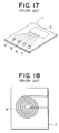
- FIG 17 shows an example of a conventional noncontacting card, which is disclosed in U.S. Pat. No.4,791,285.
- This noncontacting card 1 contains an electric circuit 3 and four coils 4 to 7 connected to this electric circuit 3.
- the coil 4 is one for receiving electric power from a terminal not shown in this figure.
- the coil 5 is one for transmitting data to a terminal.
- the coil 6 is one for receiving data from a terminal and the coil 7 is one for receiving a mode setting signal from a terminal.
- the coil 4 is formed in a spiral shape with a single wire on a printed circuit board 2. An end of the coil 4 is connected to the circuit 3 via a wire on a surface of the printed circuit board 2, and the other end is connected to the circuit 3 via a wire on the back surface of the printed circuit board 2.
- a coil holder of a terminal is shown in Figure 19.
- This coil holder 8 has an upper board 9, a vertical board 12, and a lower board 13, and has a U-like shape at its cross section.
- Spiral coils 11a and 11b are formed on the upper board 9 and the lower board 13 respectively.
- An end of each spiral coil 11a and 11b is connected to electrodes 10 and 14, respectively.
- These spiral coils 11a and 11b are also connected to each other in series via a wire formed on the vertical board 12. Only a pair of coils are shown in Figure 19, but the coil holder 8 has four pairs of coils corresponding to each of the coils 4 to 7 on the noncontacting card 1.
- a noncontacting card contains: a coil circuit having at least two circuits of spiral coils connected to each other in parallel and electromagnetically coupled with a terminal; and a processing circuit connected to the above coil circuit for performing signal processing.
- a terminal for a noncontacting card contains: a coil circuit having at least two circuits of spiral coils connected to each other in parallel and electromagnetically coupled with a noncontacting card; and a processing circuit connected to the above coil circuit for performing signal processing.
- a noncontacting transmission system comprises: a noncontacting card having a coil circuit containing at least two circuits of spiral coils connected to each other in parallel; and a terminal having a coil circuit containing at least two circuits of spiral coils connected to each other in parallel; wherein the coil circuits of the noncontacting card and the terminal are electromagnetically coupled with each other so that the terminal can achieve transmission of electric power to the noncontacting card and so that transmission and receiving of data are achieved between the terminal and the noncontacting card.
- a noncontacting card 21 of an embodiment of the present invention has a printed circuit board 23 sealed in a package 22 made of such as plastic.
- a processing circuit 24 for signal processing and first double spiral coil wires 25a and 25b are formed on a surface of the printed circuit board 23, and are formed a processing circuit 24 for signal processing and first double spiral coil wires 25a and 25b. Ends of these spiral coil wires 25a and 25b are connected to each other, and furthermore connected to a processing circuit 24. The other ends are connected to through-holes 26a and 26b, respectively, formed through a printed circuit board 23.
- second double spiral coil wires 27a and 27b Ends of these spiral coil wires 27a and 27b are connected to each other and furthermore connected to the processing circuit 24. The other ends are connected to through-holes 26a and 26b respectively. That is, the first spiral coil wires 25a and 25b are connected the second spiral coil wires 27a and 27b respectively via through-holes 26a and 26b so that two spiral coil circuits are formed which are
- spiral coils are wound so that wire 25a forms an outer winding and wire 25b forms an inner winding.
- spiral coils are wound so that wire 27a forms an inner winding and 27b forms an outer winding.
- both spiral coil circuits 28a and 28b have the same total wiring length which is the sum of the first spiral coil wire length and the second spiral coil wire length. Therefore, as shown in an equivalent circuit of Figure 4, a resistance and an inductance of the spiral circuit 28a are the same as those of the spiral circuit 28b respectively.
- Spiral coil circuits 28a and 28b connected to each other in parallel in such a manner described above constitute a coil circuit 29.
- This coil circuit 29 functions as a coil for receiving electric power from a terminal not shown in the figure as well as a coil for transmitting and receiving data signal to/from a terminal.
- the through-holes 26a and 26b form a connection means.
- These spiral coil wires 25a, 25b, 27a, and 27b are made of copper foil which is formed on the surfaces of the printed circuit board 23 and etched into a spiral shape.
- a noncontacting card of this embodiment of the present invention can perform high efficiency transmission of electric power and data signal from/to a terminal by electromagnetic coupling with a coil in a terminal, because a coil circuit 29 is composed of two spiral coil circuits 28a and 28b connected to each other in parallel. Especially, a resistance and an inductance of the coil circuit 29 can be small enough because spiral coil circuits 28a and 28b are connected to each other in parallel. As a result, the power loss is reduced and transmission using a high frequency carrier, such as higher than 1 MHz, is possible. Furthermore, equality in resistances and inductances between two spiral coil circuits 28a and 28b leads to a good balance in electromagnetic coupling with a terminal.
- both of double spiral coil wires 25a and 25b can be formed on only one surface of a printed circuit board 23, as shown in Figure 5. Ends of spiral coil wires 25a and 25b are connected to each other and further connected to a processing circuit 24, and the other ends are connected to each other and further connected, via a through-hole 26, to a wire on a back surface leading to a processing circuit 24.
- two spiral coil wires 25a and 25b, which are connected to each other in parallel, have different lengths, these two spiral coil circuits are different in resistances and inductances. However, high efficiency transmission to/from a terminal can be achieved.
- the number of spiral coil wires connected in parallel is not limited to two.
- first triple spiral coil wires 25a to 25c on a surface of a printed circuit board 23 as shown in Figure 7, and form second triple spiral coil wires 27a to 27c on the back surface of the printed circuit board 23 as shown in Figure 8, and connect, as shown in Figure 9, spiral coil wires to corresponding ones via through-holes 26a to 26c.
- spiral coil circuits 28a, 28b, and 28c composed of first and corresponding second spiral wires connected to each other, can be equal in length. Therefore, as shown in an equivalent circuit of Figure 10, spiral coil circuits 28a, 28b, and 28c are equal in resistance and inductance. In this way, more efficient transmission to/from a terminal can be achieved by increasing the number of spiral coil circuits connected in parallel.
- FIG 11 is a schematic diagram of a noncontacting transmission system for the noncontacting transmission of electric power and data signal, which has a terminal combined with a noncontacting card 21.
- a terminal has a processing circuit 30 for performing signal processing based on a preset processing sequence.
- This processing circuit 30 is connected to a spiral coil circuit 31 for making electromagnetic coupling with a coil 29 of a noncontacting card 21.
- the coil circuit 31 is made of a stranded wire 33 comprising a plurality of bundled conducting wires 32. Plural conducting wires of the stranded wire 33 are electrically insulated from each other.
- resistivity ⁇ , space permeability ⁇ o, and relative permeability of conductor ⁇ r are constants which depend just on a conductor material, and only frequency f of AC current is a variable.
- the skin depth ⁇ is plotted as a function of frequency f for various kinds of conductors in a graph of Figure 14. As can be seen from this figure, skin depth ⁇ decreases, as frequency increases. That is, current can flow only in the layer near the surface of a conductor at high frequencies.
- a stranded wire comprising a plurality of bundled fine conducting wires can transmit electric power more efficiently due to its low AC resistance than one wire having a sectional area equivalent to the total sectional area of the stranded wire.
- a processing circuit 30 of the terminal supplies AC current to the coil circuit 31. Then electromagnetic induction induces AC voltage at the coil circuit 29 of the noncontacting card 21, thus the noncontacting card 21 is turned on. After that, based on a preset processing sequence and using the coil circuit 31, the processing circuit 30 transmits or receives data signals to/from the noncontacting card 21.
- a coil circuit 31 of a terminal can be formed in such a manner that it comprises a wire wound around a ferrite core 34 which has a pair of end surfaces 35 and 36 facing each other.
- a coil circuit 29 of a noncontacting card 21 is inserted into the space between these end surfaces 35 and 36.
- the ferrite core 34 has good electrical characteristics--it has higher permeability and less magnetic reluctance than air--, effective electromagnetic coupling can be achieved between a coil circuit 31 of a terminal and a coil circuit 29 of a noncontacting card 21.
- the gap between the end surfaces 35 and 36 of a ferrite core 34 narrower one is more desirable to get effective results.
- FIG 16 shows a noncontacting transmission system composed of a combination of a noncontacting card 41 and a terminal 61.
- the noncontacting card 41 has a coil circuit 42 for receiving electric power, which is connected to a rectifier circuit 44 for performing full-wave rectification of the wave of AC power source.
- the rectifier circuit 44 is connected to a smoothing capacitor 45 for smoothing a pulsating wave flow and further connected to a processing circuit 46.
- the noncontacting card 41 has a coil circuit 47 for transmitting or receiving data signals. This coil circuit 47 is connected to the processing circuit 46 via a transistor 49. Between the coil circuit 42 and coil circuit 47, transistors 50 and 51 are provided to supply AC power induced at the coil circuit 42 to the coil circuit 47.
- the coil circuit 42 has two spiral coils 43a and 43b connected to each other via a transistor 52.
- the coil circuit 47 has two spiral coils 48a and 48b connected to each other via a transistor 53.
- the transistors 52 and 53 work as a selection means. Gates of both of these transistors are connected to the processing circuit 46.
- spiral coils 43a and 43b are connected in parallel and the coil circuit 42 functions as a spiral coil consisting of two coils in parallel.
- spiral coils 43a and 43b are cut off and the coil circuit 42 functions as a spiral coil consisting of just one coil 43a.
- the transistor 53 also operates in a similar way.
- the terminal 61 has a coil circuit 62 for transmitting electric power, which is connected to a AC generator 64, an attenuator 65, and an output voltage detector circuit 66.
- the terminal 61 also has a coil circuit 67 for transmitting and receiving data signals, which is connected to an oscillator 69 for transmitting data signals.
- the coil circuit 67 is, furthermore, connected to a waveform shaping circuit 70.
- the coil circuit 62 has two spiral coils 63a and 63b connected to each other via a switching circuit 71.
- the coil circuit 67 has two spiral coils 68a and 68b connected to each other via a switching circuit 72.
- the switching circuits 71 and 72 work as a selection means.
- spiral coils 63a and 63b are connected in series and the coil circuit 62 functions as a spiral coil consisting of two coils in parallel.
- spiral coils 63a and 63b are cut off and the coil circuit 62 functions as a spiral coil consisting just one coil 63a.
- the switching circuit 72 also operates in a similar way.
- This noncontacting transmission system operates as follows. In the following description, it is assumed that both transistors 52 and 53 of a noncontacting card 42 are on and both switching circuits 71 and 72 of the terminal 61 are closed. First, a noncontacting card 41 is inserted into a terminal 61 and the coil circuit 42 of the noncontacting card 41 is placed near the coil circuit 62 of the terminal 61. Then, the AC generator 64 of the terminal 61 generates an AC voltage. The output voltage detector circuit 66 detects the voltage across the coil circuit 62, and detected voltage is fed back to the attenuator 65 so that the detected voltage is equal to a predetermined value. Thus, the power supply to the noncontacting card 41 is maintained constant.
- signals are transmitted from the oscillator 69 of the terminal 61 via the coil circuit 67, then the coil circuit 47 of the noncontacting card 41 receives those signals by the electromagnetic induction. These received signals make the transistor 49 turn on and the signals are transmitted to the processing circuit 46.
- signals from the processing circuit 46 make transistors 50 and 51 on, and AC power is supplied to the coil circuit 47 for transmitting and receiving signals from the coil circuit 42 for receiving electric power, thus signals are transmitted to the coil circuit 67 of the terminal 61.
- the voltage detected by the output voltage detector circuit 66 of the terminal 61 rises due to the reduction in a load.
- the coil circuit 67 for transmitting and receiving signals when the received signal voltage is high, the received signal voltage can be controlled by opening the switching circuit 72.
- the signal from the processing circuit 46 makes the transistor 52 turn off so that the coil circuit 42 acts as a spiral coil consisting of just one coil 43a.
- the reception/transmission signal level can be optimized by switching the transistor 53. In this case, however, it is more effective to take the best combination of open/closed state of the switching circuit 72 of the terminal 61 and on/off state of the transistor 53 of the noncontacting card 41 to optimize the signal level.
- each of the coils 42 and 47 of the noncontacting card 41 and the coils 62 and 67 of the terminal 61 is composed of two circuits of spiral coils in parallel.
- this invention is not limited to that, but these coils can be composed of three spiral coils or more than that connected in parallel to achieve more effective transmission.
- a winding made of stranded wire, such a wire shown in Figure 12, formed on a printed circuit board can be used for coils of a noncontacting card.
- a coil made of etched copper foil can be used for coils of a terminal.
Applications Claiming Priority (2)
| Application Number | Priority Date | Filing Date | Title |
|---|---|---|---|
| JP3291462A JPH05128324A (ja) | 1991-11-07 | 1991-11-07 | 非接触カード、非接触カード用端末機及び非接触伝送システム |
| JP291462/91 | 1991-11-07 |
Publications (2)
| Publication Number | Publication Date |
|---|---|
| EP0541323A2 true EP0541323A2 (fr) | 1993-05-12 |
| EP0541323A3 EP0541323A3 (en) | 1993-12-22 |
Family
ID=17769189
Family Applications (1)
| Application Number | Title | Priority Date | Filing Date |
|---|---|---|---|
| EP19920310043 Withdrawn EP0541323A3 (en) | 1991-11-07 | 1992-11-03 | Noncontacting card, terminal and transmission system therfore |
Country Status (3)
| Country | Link |
|---|---|
| US (1) | US5436441A (fr) |
| EP (1) | EP0541323A3 (fr) |
| JP (1) | JPH05128324A (fr) |
Cited By (13)
| Publication number | Priority date | Publication date | Assignee | Title |
|---|---|---|---|---|
| FR2707410A1 (fr) * | 1993-07-09 | 1995-01-13 | Noralsy | Installation pour le stockage d'informations dans un objet portatif destiné à transmettre à distance lesdites informations ainsi stockées vers une station fixe. |
| EP0768626A1 (fr) * | 1995-10-13 | 1997-04-16 | Innovatron Industries, S.A. | Système de communication sans contact à modulation de phase et téléalimentation entre bornes et objets portatifs |
| FR2745928A1 (fr) * | 1996-03-11 | 1997-09-12 | Gemplus Card Int | Dispositif d'echange d'informations sans contact avec un ticket electronique |
| WO1997035286A1 (fr) * | 1996-03-19 | 1997-09-25 | Electrowatt Technology Innovation Ag | Systeme pour verifier des pieces de monnaie |
| EP1148406A2 (fr) * | 2000-04-10 | 2001-10-24 | Mitsubishi Denki Kabushiki Kaisha | Appareil de transmission sans contact |
| FR2820532A1 (fr) * | 2001-02-02 | 2002-08-09 | Tagproduct | Dispositif de communication sans contact avec une etiquette electronique |
| WO2002091615A1 (fr) * | 2001-05-04 | 2002-11-14 | Koninklijke Philips Electronics N.V. | Dispositif de communication a configuration de bobine permettant d'etablir une communication avec des supports de donnees fixes |
| EP1310909A1 (fr) * | 1995-06-22 | 2003-05-14 | France Telecom | Carte passive sans contact |
| EP1460712A1 (fr) * | 2003-03-17 | 2004-09-22 | Hewlett-Packard Development Company, L.P. | Verbesserte Antennenleistung durch Verwendung flexibler Leiterplatten |
| CN102074987A (zh) * | 2010-12-31 | 2011-05-25 | 科翔电子(深圳)有限公司 | 便携式通讯设备无线感应充电装置及充电方法 |
| FR2974259A1 (fr) * | 2011-04-18 | 2012-10-19 | Commissariat Energie Atomique | Recepteur alimente par une interface sans fil de type inductif |
| EP1906415A3 (fr) * | 2006-09-28 | 2015-06-03 | Broadcom Corporation | Transformateur hybride intégré/non-intégré |
| FR3028075A1 (fr) * | 2014-11-04 | 2016-05-06 | Ask Sa | Support mince de dipositif radiofrequence a l'epreuve des perforations |
Families Citing this family (40)
| Publication number | Priority date | Publication date | Assignee | Title |
|---|---|---|---|---|
| JPH0877318A (ja) * | 1994-09-08 | 1996-03-22 | Toshiba Corp | 非接触式情報記録媒体 |
| DE4432324A1 (de) * | 1994-09-13 | 1996-03-14 | Vwb Elektronik Techn Gmbh | Vorrichtung f}r eine Einrichtung zur drahtlosen Informationsabfrage und Verfahren zur Herstellung der Vorrichtung |
| JPH0962816A (ja) * | 1994-10-06 | 1997-03-07 | Mitsubishi Electric Corp | 非接触icカードおよびこれを含む非接触icカードシステム |
| JPH0981701A (ja) * | 1995-09-19 | 1997-03-28 | Toshiba Corp | 非接触式情報記録媒体および非接触式情報伝送方法 |
| US5682032A (en) * | 1996-02-22 | 1997-10-28 | Philipp; Harald | Capacitively coupled identity verification and escort memory apparatus |
| US5834756A (en) * | 1996-06-03 | 1998-11-10 | Motorola, Inc. | Magnetically communicative card |
| US5847447A (en) * | 1996-07-09 | 1998-12-08 | Ambient Corporation | Capcitively coupled bi-directional data and power transmission system |
| DE19629646C2 (de) * | 1996-07-23 | 1998-09-10 | Wolf Gmbh Richard | Verfahren und Vorrichtung zur automatischen Identifikation von Komponenten medizinischer Gerätesysteme |
| DE19649761C2 (de) * | 1996-11-30 | 2003-04-03 | Univ Stuttgart | Verfahren zur Herstellung von Flüssigkristall-Displays auf Kunststoff-Folien unter Verwendung von bistabilen Flüssigkristallen |
| JPH10203066A (ja) * | 1997-01-28 | 1998-08-04 | Hitachi Ltd | 非接触icカード |
| FI971180A (fi) * | 1997-03-20 | 1998-12-23 | Micronas Oy | Stripe-line-kela |
| EP0967568B1 (fr) * | 1998-06-23 | 2006-08-30 | Meto International GmbH | Elément d'identification |
| EP0971306A1 (fr) * | 1998-07-10 | 2000-01-12 | Microchip Technology Inc. | Bobine universelle pour la programmation d'étiquettes ayant différentes configurations |
| US6173897B1 (en) * | 1998-07-27 | 2001-01-16 | John W. Halpern | Universal card interface module for contact free cards |
| US6837438B1 (en) * | 1998-10-30 | 2005-01-04 | Hitachi Maxell, Ltd. | Non-contact information medium and communication system utilizing the same |
| EP1304007A1 (fr) * | 2000-05-26 | 2003-04-23 | Cegetel Groupe | Procede de dialogue entre un module d'identification d'abonne, cooperant avec un terminal au sein d'un radiotelephone, et un dispositif local |
| AUPR188600A0 (en) * | 2000-12-05 | 2001-01-04 | Vfj Technology Pty Limited | A smart token and reader device |
| KR20010044484A (ko) * | 2001-02-26 | 2001-06-05 | 노명래 | 스마트카드 |
| EP1484712B1 (fr) * | 2002-03-11 | 2011-08-10 | Universal Entertainment Corporation | Carte a circuit integre |
| JP2006215589A (ja) * | 2003-04-30 | 2006-08-17 | Brother Ind Ltd | 通信装置及び無線タグリーダー/ライター |
| DE102004006504A1 (de) * | 2004-02-10 | 2005-09-08 | Infineon Technologies Ag | Kontaktloser Datenträger mit Signalgeber |
| US7503491B2 (en) * | 2005-10-29 | 2009-03-17 | Magnex Corporation | RFID chip and antenna with improved range |
| US7793839B2 (en) | 2006-08-07 | 2010-09-14 | Smart Wave Technologies Corporation | System enabling the exchange of information between products |
| US7504705B2 (en) * | 2006-09-29 | 2009-03-17 | International Business Machines Corporation | Striped on-chip inductor |
| JP5174424B2 (ja) | 2007-10-24 | 2013-04-03 | デクセリアルズ株式会社 | アンテナ回路及びその抵抗低減方法、並びにトランスポンダ |
| US7926728B2 (en) * | 2007-10-31 | 2011-04-19 | Infineon Technologies Ag | Integrated circuit device including a contactless integrated circuit inlay |
| JP2008090863A (ja) * | 2007-12-11 | 2008-04-17 | Hitachi Chem Co Ltd | Icカード |
| JP2009158598A (ja) * | 2007-12-25 | 2009-07-16 | Panasonic Electric Works Co Ltd | 平面コイル及びこれを用いた非接触電力伝送機器 |
| JP5433199B2 (ja) * | 2008-10-21 | 2014-03-05 | 学校法人慶應義塾 | 電子回路 |
| US9130395B2 (en) | 2008-12-12 | 2015-09-08 | Hanrim Postech Co., Ltd. | Non-contact charging station with planar spiral power transmission coil and method for controlling the same |
| CN101828320B (zh) * | 2008-12-12 | 2013-04-10 | 郑春吉 | 非接触充电站、非接触受电装置及其控制方法 |
| KR100928439B1 (ko) * | 2008-12-12 | 2009-11-24 | 정춘길 | 평면나선형 코어구조의 파워트랜스피씨비코어가 구비된 무접점전력충전스테이션 |
| JP2010277609A (ja) * | 2010-09-01 | 2010-12-09 | Hitachi Chem Co Ltd | Icカード |
| JP5354137B1 (ja) * | 2012-01-30 | 2013-11-27 | 株式会社村田製作所 | 無線icデバイス |
| CN102545356A (zh) * | 2012-02-22 | 2012-07-04 | 浙江大学 | 一种植入式无线充电扩展设备 |
| US9214936B2 (en) * | 2013-06-18 | 2015-12-15 | Hyundai Motor Company | Non-contact sensing module and method of manufacturing the same |
| US11264708B2 (en) * | 2015-01-27 | 2022-03-01 | At&S Austria Technologie & Systemtechnik Aktiengesellschaft | Component carrier with integrated antenna structure |
| EP3449532B1 (fr) | 2016-04-28 | 2024-02-28 | AT & S Austria Technologie & Systemtechnik Aktiengesellschaft | Porte-composant à agencement d'antenne intégré, appareil électronique et procédé de radiocommunication |
| JP2020027813A (ja) * | 2018-08-09 | 2020-02-20 | 矢崎総業株式会社 | 電力伝送ユニット |
| JP2021057377A (ja) * | 2019-09-27 | 2021-04-08 | 株式会社オートネットワーク技術研究所 | インダクタ |
Citations (5)
| Publication number | Priority date | Publication date | Assignee | Title |
|---|---|---|---|---|
| US2843829A (en) * | 1952-12-30 | 1958-07-15 | Du Mont Allen B Lab Inc | Electrical inductance |
| US4791285A (en) * | 1985-07-03 | 1988-12-13 | Koatsu Gas Kogyo Co., Ltd. | Read/write method by a non-contact system and between a storage substrate and read/write unit |
| JPH01150305A (ja) * | 1987-12-08 | 1989-06-13 | Kaoru Umeya | 超伝導磁石用コイル及びその製造方法 |
| US4960983A (en) * | 1987-09-28 | 1990-10-02 | Mitsubishi Denki Kabushiki Kaisha | Noncontact type IC card and system for noncontact transfer of information using the same |
| JPH04137606A (ja) * | 1990-09-28 | 1992-05-12 | Toshiba Lighting & Technol Corp | 平面状巻線 |
Family Cites Families (15)
| Publication number | Priority date | Publication date | Assignee | Title |
|---|---|---|---|---|
| US3845437A (en) * | 1973-05-17 | 1974-10-29 | Allis Chalmers | Series-multiple transformer having non-integer series-parallel voltage ratio |
| FR2527832A1 (fr) * | 1982-05-25 | 1983-12-02 | Barthelemy Louis | Transformateur electrique a circuits primaires modulaires alimentes selectivement |
| JPS6151286A (ja) * | 1984-08-18 | 1986-03-13 | Tdk Corp | カ−ド用トランス |
| US4818855A (en) * | 1985-01-11 | 1989-04-04 | Indala Corporation | Identification system |
| GB8509135D0 (en) * | 1985-04-10 | 1985-05-15 | Gen Electric Co Plc | Transaction system |
| JPH0751391B2 (ja) * | 1985-07-11 | 1995-06-05 | 東京磁気印刷株式会社 | Icカ−ド |
| JPS62134780A (ja) * | 1985-12-09 | 1987-06-17 | Hitachi Ltd | 非接触icカ−ド |
| JPS62161058A (ja) * | 1986-01-10 | 1987-07-17 | Copyer Co Ltd | モ−タの回転速度検出方法 |
| EP0249356B1 (fr) * | 1986-05-26 | 1991-07-24 | Kabushiki Kaisha Toshiba | Carte de données à dispositif de transfert de signaux de manière inductive |
| JPS6357295A (ja) * | 1986-08-29 | 1988-03-11 | 株式会社東芝 | 薄膜電磁変換器 |
| US4791283A (en) * | 1986-06-03 | 1988-12-13 | Intellicard International, Inc. | Transaction card magnetic stripe emulator |
| JPS63116412A (ja) * | 1986-11-05 | 1988-05-20 | Fujikura Ltd | プリントコイルとそのインダクタンス調整方法 |
| JPS6491290A (en) * | 1987-10-01 | 1989-04-10 | Nippon Chemicon | Driving circuit of head core in ic card reader writer |
| JP2735295B2 (ja) * | 1988-09-30 | 1998-04-02 | 株式会社東芝 | 平面インダクタ |
| US5198647A (en) * | 1989-11-28 | 1993-03-30 | Mitsubishi Denki Kabushiki Kaisha | Plural-coil non-contact ic card having pot cores and shielding walls |
-
1991
- 1991-11-07 JP JP3291462A patent/JPH05128324A/ja active Pending
-
1992
- 1992-10-21 US US07/964,262 patent/US5436441A/en not_active Expired - Fee Related
- 1992-11-03 EP EP19920310043 patent/EP0541323A3/en not_active Withdrawn
Patent Citations (5)
| Publication number | Priority date | Publication date | Assignee | Title |
|---|---|---|---|---|
| US2843829A (en) * | 1952-12-30 | 1958-07-15 | Du Mont Allen B Lab Inc | Electrical inductance |
| US4791285A (en) * | 1985-07-03 | 1988-12-13 | Koatsu Gas Kogyo Co., Ltd. | Read/write method by a non-contact system and between a storage substrate and read/write unit |
| US4960983A (en) * | 1987-09-28 | 1990-10-02 | Mitsubishi Denki Kabushiki Kaisha | Noncontact type IC card and system for noncontact transfer of information using the same |
| JPH01150305A (ja) * | 1987-12-08 | 1989-06-13 | Kaoru Umeya | 超伝導磁石用コイル及びその製造方法 |
| JPH04137606A (ja) * | 1990-09-28 | 1992-05-12 | Toshiba Lighting & Technol Corp | 平面状巻線 |
Non-Patent Citations (2)
| Title |
|---|
| PATENT ABSTRACTS OF JAPAN vol. 13, no. 410 (E-819)11 September 1989 & JP-A-01 150 305 ( KAORU UMEYA ) * |
| PATENT ABSTRACTS OF JAPAN vol. 16, no. 408 (E-1255)28 August 1992 & JP-A-04 137 606 ( TOSHIBA LIGHTING & TECHNOL. ) * |
Cited By (21)
| Publication number | Priority date | Publication date | Assignee | Title |
|---|---|---|---|---|
| FR2707410A1 (fr) * | 1993-07-09 | 1995-01-13 | Noralsy | Installation pour le stockage d'informations dans un objet portatif destiné à transmettre à distance lesdites informations ainsi stockées vers une station fixe. |
| EP1310909A1 (fr) * | 1995-06-22 | 2003-05-14 | France Telecom | Carte passive sans contact |
| EP0768626A1 (fr) * | 1995-10-13 | 1997-04-16 | Innovatron Industries, S.A. | Système de communication sans contact à modulation de phase et téléalimentation entre bornes et objets portatifs |
| FR2739955A1 (fr) * | 1995-10-13 | 1997-04-18 | Innovatron Ind Sa | Systeme de communication sans contact a modulation de phase et telealimentation entre bornes et objets portatifs |
| FR2745928A1 (fr) * | 1996-03-11 | 1997-09-12 | Gemplus Card Int | Dispositif d'echange d'informations sans contact avec un ticket electronique |
| WO1997034249A1 (fr) * | 1996-03-11 | 1997-09-18 | Gemplus S.C.A. | Dispositif d'echange d'informations sans contact avec un ticket electronique |
| WO1997035286A1 (fr) * | 1996-03-19 | 1997-09-25 | Electrowatt Technology Innovation Ag | Systeme pour verifier des pieces de monnaie |
| US6065582A (en) * | 1996-03-19 | 2000-05-23 | Electrowatt Technology Innovation Ag | Coin-checking arrangement |
| US6792246B2 (en) | 2000-04-10 | 2004-09-14 | Mitsubishi Denki Kabushiki Kaisha | Noncontact transmitting apparatus |
| EP1148406A2 (fr) * | 2000-04-10 | 2001-10-24 | Mitsubishi Denki Kabushiki Kaisha | Appareil de transmission sans contact |
| EP1148406A3 (fr) * | 2000-04-10 | 2002-06-19 | Mitsubishi Denki Kabushiki Kaisha | Appareil de transmission sans contact |
| FR2820532A1 (fr) * | 2001-02-02 | 2002-08-09 | Tagproduct | Dispositif de communication sans contact avec une etiquette electronique |
| WO2002091615A1 (fr) * | 2001-05-04 | 2002-11-14 | Koninklijke Philips Electronics N.V. | Dispositif de communication a configuration de bobine permettant d'etablir une communication avec des supports de donnees fixes |
| EP1460712A1 (fr) * | 2003-03-17 | 2004-09-22 | Hewlett-Packard Development Company, L.P. | Verbesserte Antennenleistung durch Verwendung flexibler Leiterplatten |
| US6924777B2 (en) | 2003-03-17 | 2005-08-02 | Hewlett-Packard Development Company, L.P. | Enhanced antenna using flexible circuitry |
| EP1906415A3 (fr) * | 2006-09-28 | 2015-06-03 | Broadcom Corporation | Transformateur hybride intégré/non-intégré |
| CN102074987A (zh) * | 2010-12-31 | 2011-05-25 | 科翔电子(深圳)有限公司 | 便携式通讯设备无线感应充电装置及充电方法 |
| FR2974259A1 (fr) * | 2011-04-18 | 2012-10-19 | Commissariat Energie Atomique | Recepteur alimente par une interface sans fil de type inductif |
| EP2515446A1 (fr) | 2011-04-18 | 2012-10-24 | Commissariat à l'Énergie Atomique et aux Énergies Alternatives | Récepteur alimenté par une interface sans fil de type inductif |
| FR3028075A1 (fr) * | 2014-11-04 | 2016-05-06 | Ask Sa | Support mince de dipositif radiofrequence a l'epreuve des perforations |
| WO2016071584A1 (fr) * | 2014-11-04 | 2016-05-12 | Ask | Support mince et flexible de dispositif radiofréquence à l'épreuve des perforations |
Also Published As
| Publication number | Publication date |
|---|---|
| EP0541323A3 (en) | 1993-12-22 |
| JPH05128324A (ja) | 1993-05-25 |
| US5436441A (en) | 1995-07-25 |
Similar Documents
| Publication | Publication Date | Title |
|---|---|---|
| US5436441A (en) | Noncontacting card, noncontacting-card terminal and noncontacting transmission system | |
| US8125208B2 (en) | Transformer device utilizing an air gap for non-contact energy transmission from the primary side to the secondary side | |
| CN110415954B (zh) | 优化发射以及用于无线电力传输的发射/接收trx线圈 | |
| US20210151250A1 (en) | Coil Module, Wireless Charging Transmitting Apparatus, Wireless Charging Receiving Apparatus, Wireless Charging System, and Mobile Terminal | |
| CN110289156B (zh) | 线圈绕组、线圈模组、发射装置、接收装置、系统和终端 | |
| CN108321914B (zh) | 一种线圈及无线充电接收装置、与发射装置与系统 | |
| EP0547120B1 (fr) | Transfomateurs de puissance et inducteurs couples avec entrelacement optimal d'enroulement | |
| JP2001085248A (ja) | トランス | |
| EP1160801B1 (fr) | Ensemble câble multiconducteur à haute fréquence et équipment d'alimentation électique pour un ou plusieurs corps mobiles utilisant un tel câble | |
| JPH1197263A (ja) | 非接触式電力伝送装置およびそれに使用される渦巻型コイル | |
| EP0410526A1 (fr) | Générateur de tension électrique | |
| JPH11176676A (ja) | 小型非接触伝送装置 | |
| RU2108649C1 (ru) | Способ питания электротехнических устройств и устройство для его осуществления | |
| EP0788216A2 (fr) | Filtre pour un circuit d'entraînement d'un moteur | |
| WO2021131607A1 (fr) | Dispositif de détection d'objet étranger, dispositif de transmission d'énergie, dispositif de réception d'énergie et système de transmission d'énergie | |
| US11176294B2 (en) | Method of designing coils for transmitting or receiving power wirelessly | |
| JP7222675B2 (ja) | 無線装置 | |
| EP0497556A1 (fr) | Dispositif de bobine imprimée pour circuit d'accord double | |
| US1843525A (en) | Feeding arrangement for electric devices | |
| EP0196341A1 (fr) | Montage de bobine commandée électroniquement | |
| JP2520057B2 (ja) | トランス装置 | |
| CN217468172U (zh) | 变压器、电源转换电路及适配器 | |
| CN214753198U (zh) | 线圈绕组、线圈模组、发射装置以及接收装置 | |
| US20040169576A1 (en) | Electronic inductive and capacitive component | |
| CN111627677A (zh) | 无线充电线圈、无线充电装置及无线充电线圈的绕制方法 |
Legal Events
| Date | Code | Title | Description |
|---|---|---|---|
| PUAI | Public reference made under article 153(3) epc to a published international application that has entered the european phase |
Free format text: ORIGINAL CODE: 0009012 |
|
| AK | Designated contracting states |
Kind code of ref document: A2 Designated state(s): DE FR GB |
|
| PUAL | Search report despatched |
Free format text: ORIGINAL CODE: 0009013 |
|
| AK | Designated contracting states |
Kind code of ref document: A3 Designated state(s): DE FR GB |
|
| 17P | Request for examination filed |
Effective date: 19940609 |
|
| 17Q | First examination report despatched |
Effective date: 19941124 |
|
| RTI1 | Title (correction) |
Free format text: NONCONTACTING CARD AND NONCONTACTING CARD TERMINAL |
|
| RTI1 | Title (correction) |
Free format text: NONCONTACTING CARD AND NONCONTACTING CARD TERMINAL |
|
| STAA | Information on the status of an ep patent application or granted ep patent |
Free format text: STATUS: THE APPLICATION IS DEEMED TO BE WITHDRAWN |
|
| 18D | Application deemed to be withdrawn |
Effective date: 20020209 |