EP0534422A2 - Dispositif d'alimentation - Google Patents
Dispositif d'alimentation Download PDFInfo
- Publication number
- EP0534422A2 EP0534422A2 EP92116340A EP92116340A EP0534422A2 EP 0534422 A2 EP0534422 A2 EP 0534422A2 EP 92116340 A EP92116340 A EP 92116340A EP 92116340 A EP92116340 A EP 92116340A EP 0534422 A2 EP0534422 A2 EP 0534422A2
- Authority
- EP
- European Patent Office
- Prior art keywords
- circuit
- inductor
- switching element
- terminal
- diode
- Prior art date
- Legal status (The legal status is an assumption and is not a legal conclusion. Google has not performed a legal analysis and makes no representation as to the accuracy of the status listed.)
- Granted
Links
Images


Classifications
-
- H—ELECTRICITY
- H02—GENERATION; CONVERSION OR DISTRIBUTION OF ELECTRIC POWER
- H02M—APPARATUS FOR CONVERSION BETWEEN AC AND AC, BETWEEN AC AND DC, OR BETWEEN DC AND DC, AND FOR USE WITH MAINS OR SIMILAR POWER SUPPLY SYSTEMS; CONVERSION OF DC OR AC INPUT POWER INTO SURGE OUTPUT POWER; CONTROL OR REGULATION THEREOF
- H02M3/00—Conversion of dc power input into dc power output
- H02M3/02—Conversion of dc power input into dc power output without intermediate conversion into ac
- H02M3/04—Conversion of dc power input into dc power output without intermediate conversion into ac by static converters
- H02M3/10—Conversion of dc power input into dc power output without intermediate conversion into ac by static converters using discharge tubes with control electrode or semiconductor devices with control electrode
- H02M3/145—Conversion of dc power input into dc power output without intermediate conversion into ac by static converters using discharge tubes with control electrode or semiconductor devices with control electrode using devices of a triode or transistor type requiring continuous application of a control signal
- H02M3/155—Conversion of dc power input into dc power output without intermediate conversion into ac by static converters using discharge tubes with control electrode or semiconductor devices with control electrode using devices of a triode or transistor type requiring continuous application of a control signal using semiconductor devices only
Definitions
- This invention relates to a constant-voltage power supply device of a continuous current mode and, more particularly, to a power supply device of this type capable of performing functions of conventional power supply devices of BUCK, BOOST and BUCK-BOOSt types with a single circuit system.
- a BUCK type (voltage drop type) circuit shown in Fig. 17 As conventional constant-voltage power supply circuits, a BUCK type (voltage drop type) circuit shown in Fig. 17, a BOOST type (voltage rising type) circuit shown in Fig. 18 and a BUCK-BOOST type circuit shown in Fig. 19 are well known and widely used.
- a power source E a load resistance RL
- a switching element S1 a diode D1
- a capacitor C1 capacitor C1 and inductors L11, L12 and L21.
- the switching element S1 In the BUCK type circuit, the switching element S1 is connected in series to the inductor L11 and the diode d1 is connected between the switching element S1 and the inductor L11 in T-shape.
- the inductor L12 and the diode D1 is connected in series and the switching element S1 is connected between the inductor L12 and the diode D1 in T-shape.
- the switching element S1 is connected in series to the diode D1 and the inductor L21 is connected between the the switching element S1 and the diode D1 in T-shape.
- a CUK (inverted polarity) type converter as shown in Fig. 20 has been proposed and used to overcome the above described problem.
- This CUK converter is advantageous in that generation of noise is reduced because this converter is a continuous current mode both at its input and output.
- the CUK converter corresponds in function to the BUCK-BOOST type circuit, it is not frequently used because this converter operates as an inverted polarity type circuit, i.e., the output becomes a negative voltage when the input is a positive voltage.
- the BUCK type circuit is most frequently used as a constant-voltage power supply circuit because, in the BUCK type circuit, duty factor of the switching element S1 can be changed freely between 0% and 100% and, therefore, the circuit is easy to control and is capable of providing a high efficiency.
- the BOOST type circuit as a frequently used constant-voltage power supply circuit and the CUK type converter which is not used except when a voltage of an opposite polarity is required for some reason has the least chance of being used.
- the CUK type converter is advantageous in preventing generation of a noise because its input and output are of a continuous current mode but it is difficult to substitute the BUCK type or BOOST type circuit by the CUK converter because the polarity is inverted between the input and the output.
- For substituting the BUCK type circuit by the CUK converter it is desirable that duty factor can be used up to 100%.
- the BOOST type, BUCK-BOOST type and the CUK type circuits have restriction in duty factor and, when duty factor becomes 100%, the switching element S1 is destroyed.
- the CUK type converter Although the polarity of voltage is inverted in the CUK type converter as in the BUCK-BOOST type circuit, its output voltage can be controlled at a higher or lower level than its input voltage and, therefore, the CUK type converter can be used both for increasing and decreasing voltage. Accordingly, in the present situation, when a voltage increasing or decreasing circuit of a continuous current mode at both input and output terminals is required, there is no alternative but to use the CUK converter with the limitation that its polarity of voltage is inverted between its input and output.
- an object of the invention to provide a converter type power supply device having two continuous current modes at its input and output corresponding to each of the BUCK, BOOST and BUCK-BOOST type circuits, totalling six continuous current modes.
- a power supply device of four-channel circuit type having an input terminal, an output terminal and a ground terminal comprises a first inductance, one end of which is connected to the input terminal, a second inductance, one end of which is connected to the ground terminal, a converter circuit connected to the other end of the first inductance through an input side of the converter circuit and connected to the other end of the second inductance through a ground side thereof.
- the converter circuit comprises a series circuit of a capacitor and a diode and a switching element connected in parallel to the series circuit, the first inductor being connected between the converter circuit and the input terminal, and the second inductor being connected between a connecting point of the capacitor and the diode and the ground terminal.
- the converter circuit comprises a series circuit of a capacitor and a switching element and a diode connected in parallel to the series circuit, the first inductor being connected between the converter circuit and the input teminal, and the second inductor being connected between a connecting point of the switching element and the capacitor and the ground terminal.
- the converter in the power supply device, comprises a series circuit of a switching element and a diode and a capacitor connected in parallel to the series circuit, the first inductor being connected between the converter circuit and the input terminal, and the second inductor being connected between a connecting point of the switching element and the diode and the ground terminal.
- the converter circuit comprises a series circuit of a capacitor and a diode and a switching element connected in parallel to the series circuit, the first inductor being connected between the converter circuit and the output terminal, and the second inductor being connected between a connecting point of the capacitor and the diode and the ground terminal.
- the converter circuit comprises a series circuit of a capacitor and a switching element and a diode connected in parallel to the series circuit, the first inductor being connected between the converter circuit and the output terminal, and the second inductor being connected between a connecting point of the switching element and the capacitor and the ground terminal.
- the converter circuit comprises a series circuit of a switching element and a diode and a capacitor connected in parallel to the series circuit, the first inductor being connected between the converter circuit and the output terminal, and the second inductor being connected between a connecting point of the switching element and the diode and the ground terminal.
- Fig. 1 shows a first basic principle of the device according to the invention.
- a first inductor L1 is connected between an input terminal 10 and a converter circuit CONV and a second inductor L2 is connected between the converter circuit CONV and a ground terminal 11.
- Reference character 12 designates an output terminal.
- Fig. 2 shows a second basic principle of the device according to the invention.
- a first inductor L1 is connected between a converter circuit COMV and an ouput terminal 12 and a second inductor L2 is connected between the converter circuit CONV and a ground terminal 11.
- a BUCK type circuit has, as shown in Fig. 22, an inductor L11 connected in series on the side of the output terminal 12 so that an output current IOUT becomes a continuous mode due to reactance of the inductor L11.
- a BOOST type circuit has, as shown in Fig. 23, an inductor L12 connected in series on the side of the input terminal 10 so that an input current IIN becomes a continuous mode due to reactance of the inductor L12.
- a CUK type circuit as shown in Fig. 24 is obtained.
- this CUK type circuit it is necessary to determine an input current IIN and an output current IOUT at opposite directions to each other, since in the CUK type circuit, transmission of energy is not achieved unless current flowing to the capacitor C1 alternates.
- this is achieved by connecting the BUCK circuit on the output side in an opposite polarity and, therefore, the CUK type circuit can be operated only as an inverted polarity type circuit. If the polarity of the diode D1 is set one opposite to the one shown in the figure for preventing inversion of the polarity, an expected operation will not be realized because the direction of current flowing to the capacitor C1 will not alternate but become unidirectional.
- the CUK type circuit is made, as described above, on the basis of concept that the inductors L12 and L11 are connected in series to the input and output terminals 10 and 12 and input and output currents are caused to have a continuous mode due to reactance of these inductors, the CUK type circuit can be expressed by Fig. 5.
- a feature of the present invention resides in that, as shown in Figs. 1 and 2, the first inductor L1 is connected in series only on one side of the converter CONV, i.e., either the side of the input terminal 10 or the side of the output terminal 12 and the second inductor L2 is connected between the converter CONV and the ground terminal 11.
- the circuit of the invention is made on the basic concept that a continuous current mode in both input and output currents can be realized even if there are no inductors both on input and output sides simultaneously.
- the CUK type converter is a single circuit whereas the circuit of the present invention can realize six types of continuous mode converters as will be described later. According to these circuits realized by the invention, there are two types of circuits corresponding in function to each of the BUCK type, BOOST type and BUCK-BOOST type circuits and, this is advantageous from the standpoint of practical application of the invention.
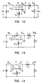
- Figs. 1 to 3 show the first to third embodiments of the invention.
- a common feature of these first to third embodiments is that a first inductor L1 is connected in series between a converter circuit and an input terminal 10 and a second inductor L2 is connected between the converter circuit and a ground terminal 11.
- the converter circuit is constructed of a switching element S1, a capacitor C1 and a diode D1.
- the embodiment of Fig. 3 corresponds to the BUCK type circuit
- the embodiment of Fig. 4 to the BOOST type circuit
- the embodiment of Fig. 5 to the BUCK-BOOST type circuit respectively.
- Figs. 6 to 8 show the fourth to fifth embodiments of the invention.
- a common feature of these embodiments is that a first inductor L1 is connected in series between a converter circuit and an output terminal 12 and a second inductor L2 is connected between the converter circuit and a ground terminal 11.
- the converter circuit is constructed of a switching element S1, a capacitor C1 and a diode D1.
- the embodiment of Fig. 6 corresponds to the BUCK type circuit
- the embodiment of Fig. 7 to the BOOST type circuit
- the embodiment of Fig. 8 to the BUCK-BOOST type circuit respectively.
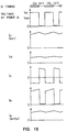
- Figs. 9 to 14 are diagrams for describing the operations of the embodiments of Figs. 3 to 8.
- Fig. 9 will be described with reference to the waveform diagram of Fig. 15.
- impedance of the capacitor C1 is assumed to be sufficiently small at a switching frequency.
- an ouptut current IOUT is provided from the diode D1 alternately through the switching element S1 when the switching element is on and through the diode D1 when the switching element S1 is off.
- Current ID1 flowing through the diode D1 is supplied from the inductor L2 and the capacitor C1 but only from the inductor L2 as a dc, so that average current of ID1 is IL2.
- the output current IOUT is a sum of the currents IL1 and IL2 regardless whether the switching element S1 is on or off whereby a continuous current mode is brought about.
- the input current IIN is the current IL1 itself so that it is originally continuous.
- Current IC1 to the capacitor C1 alternates and voltage across the capacitor C1 is maintained substantially at a constant voltage VIN.
- voltage across the inductor L1 is not equal to voltage across the inductor L2 and, therefore, the circuit requires two coils. Since voltage across the inductor L1 is small, inductance of the inductors L1 and L2 may be L2 ⁇ L1.
- Output current IOUT is current IL1 itself and the circuit is of a continuous current mode.
- Current IL2 is an average current of IS1.
- Fig. 26 shows a basic principle of a switch inverter type power supply circuit of U.S. Patent Application Serial No. 07/896,214 invented by the same inventor as the present application.
- the power supply circuit includes a dc power source, switching means 2 including a switching element which can be turned on and off at a desired timing for switching the dc power source 1 to convert a dc to an ac, dc output means for full wave rectifying an ac input supplied and smoothing it by a capacitor and outputting it as a dc output, series resonance means 4 (Lb, Cb) formed in series to current flowing to an output terminal of the switching means 2 and parallel resonance means 5 (La, Ca) formed in parallel to voltage produced at the output terminal of the switching means 2, and switching control means 6 for intermittently turning on and off the switching means 2.
- switching means 2 including a switching element which can be turned on and off at a desired timing for switching the dc power source 1 to convert a dc to an ac
- this resonance type power supply circuit turning on of the switching element is made at a zero-voltage state and turning off of the switching element is made at a zero-current state whereby switching loss is reduced and efficiency of the circuit is improved.
- series resonance current and parallel resonance voltage have a spectrum which is nearly a single frequency and, as a result, possibility of causing ringing or overshoot by interference with resonance dip in some parts of the circuit is reduced and unnecessary radiation such as harmonics is reduced. Since, however, this resonance type power supply circuit has no stabilizing function, stabilization of its output voltage can be realized by connecting the circuit of the present invention to the secondary side of the resonance type power supply circuit.
Applications Claiming Priority (2)
| Application Number | Priority Date | Filing Date | Title |
|---|---|---|---|
| JP273362/91 | 1991-09-25 | ||
| JP3273362A JP2522128B2 (ja) | 1991-09-25 | 1991-09-25 | 電源装置 |
Publications (3)
| Publication Number | Publication Date |
|---|---|
| EP0534422A2 true EP0534422A2 (fr) | 1993-03-31 |
| EP0534422A3 EP0534422A3 (en) | 1995-05-24 |
| EP0534422B1 EP0534422B1 (fr) | 1997-12-10 |
Family
ID=17526846
Family Applications (1)
| Application Number | Title | Priority Date | Filing Date |
|---|---|---|---|
| EP92116340A Expired - Lifetime EP0534422B1 (fr) | 1991-09-25 | 1992-09-24 | Dispositif d'alimentation |
Country Status (3)
| Country | Link |
|---|---|
| EP (1) | EP0534422B1 (fr) |
| JP (1) | JP2522128B2 (fr) |
| DE (1) | DE69223477T2 (fr) |
Cited By (8)
| Publication number | Priority date | Publication date | Assignee | Title |
|---|---|---|---|---|
| EP0684754A1 (fr) * | 1994-05-24 | 1995-11-29 | MAGNETI MARELLI S.p.A. | Alimentation, en particulier pour véhicules |
| EP0766371A2 (fr) * | 1995-09-27 | 1997-04-02 | Kabushiki Kaisha Toshiba | Petite alimentation de courant continu |
| EP0768812A2 (fr) * | 1995-10-16 | 1997-04-16 | General Electric Company | Ballast électronique à facteur de puissance élevé |
| WO2001091273A2 (fr) * | 2000-05-19 | 2001-11-29 | Telefonaktiebolaget Lm Ericsson (Publ) | Convertisseurs continu-continu |
| WO2003090336A1 (fr) * | 2002-04-19 | 2003-10-30 | Linak A/S | Dispositif de commande, de preference un actionneur, commande et procede de construction |
| EP2317635A1 (fr) * | 2009-11-02 | 2011-05-04 | ABB Research Ltd | Ensemble de convertisseur CC-CC non isolé |
| CN105593778A (zh) * | 2013-09-20 | 2016-05-18 | 凌力尔特有限公司 | 用于连接电子系统中的两个节点的开关拓扑 |
| CN108432110A (zh) * | 2015-12-22 | 2018-08-21 | 诺乌姆工程有限公司 | Dc/dc转换器 |
Families Citing this family (2)
| Publication number | Priority date | Publication date | Assignee | Title |
|---|---|---|---|---|
| US8704504B2 (en) * | 2010-09-03 | 2014-04-22 | Semiconductor Energy Laboratory Co., Ltd. | Power supply circuit comprising detection circuit including reference voltage circuits as reference voltage generation circuits |
| WO2016113915A1 (fr) * | 2015-01-16 | 2016-07-21 | 新電元工業株式会社 | Convertisseur élévateur/abaisseur |
Citations (1)
| Publication number | Priority date | Publication date | Assignee | Title |
|---|---|---|---|---|
| FR2647980A1 (fr) * | 1989-06-02 | 1990-12-07 | Europ Agence Spatiale | Convertisseur electrique a plusieurs bobines d'induction |
Family Cites Families (2)
| Publication number | Priority date | Publication date | Assignee | Title |
|---|---|---|---|---|
| JPS5719819A (en) * | 1980-07-09 | 1982-02-02 | Fujitsu Ltd | Switching regulator circuit |
| JPS57101591U (fr) * | 1980-12-10 | 1982-06-22 |
-
1991
- 1991-09-25 JP JP3273362A patent/JP2522128B2/ja not_active Expired - Fee Related
-
1992
- 1992-09-24 EP EP92116340A patent/EP0534422B1/fr not_active Expired - Lifetime
- 1992-09-24 DE DE1992623477 patent/DE69223477T2/de not_active Expired - Fee Related
Patent Citations (2)
| Publication number | Priority date | Publication date | Assignee | Title |
|---|---|---|---|---|
| FR2647980A1 (fr) * | 1989-06-02 | 1990-12-07 | Europ Agence Spatiale | Convertisseur electrique a plusieurs bobines d'induction |
| WO1990015469A1 (fr) * | 1989-06-02 | 1990-12-13 | Agence Spatiale Europeenne | Convertisseur electrique a plusieurs bobines d'induction |
Non-Patent Citations (1)
| Title |
|---|
| IEEE TRANSACTIONS ON POWER ELECTRONICS, vol. 1,no. 6, pages 151-157, XP 000175329 DRAGAN MAKSIMOVIC ET AL 'SWITCHING CONVERTERS WITH WIDE DC CONVERSION RANGE' * |
Cited By (18)
| Publication number | Priority date | Publication date | Assignee | Title |
|---|---|---|---|---|
| EP0684754A1 (fr) * | 1994-05-24 | 1995-11-29 | MAGNETI MARELLI S.p.A. | Alimentation, en particulier pour véhicules |
| EP0766371A2 (fr) * | 1995-09-27 | 1997-04-02 | Kabushiki Kaisha Toshiba | Petite alimentation de courant continu |
| EP0766371A3 (fr) * | 1995-09-27 | 1999-03-17 | Kabushiki Kaisha Toshiba | Petite alimentation de courant continu |
| EP0768812A2 (fr) * | 1995-10-16 | 1997-04-16 | General Electric Company | Ballast électronique à facteur de puissance élevé |
| EP0768812A3 (fr) * | 1995-10-16 | 1998-04-01 | General Electric Company | Ballast électronique à facteur de puissance élevé |
| WO2001091273A2 (fr) * | 2000-05-19 | 2001-11-29 | Telefonaktiebolaget Lm Ericsson (Publ) | Convertisseurs continu-continu |
| WO2001091273A3 (fr) * | 2000-05-19 | 2002-05-10 | Ericsson Telefon Ab L M | Convertisseurs continu-continu |
| WO2003090336A1 (fr) * | 2002-04-19 | 2003-10-30 | Linak A/S | Dispositif de commande, de preference un actionneur, commande et procede de construction |
| EP2317635A1 (fr) * | 2009-11-02 | 2011-05-04 | ABB Research Ltd | Ensemble de convertisseur CC-CC non isolé |
| CN102055316A (zh) * | 2009-11-02 | 2011-05-11 | Abb研究有限公司 | 非隔离直流-直流转换器组件 |
| CN102055316B (zh) * | 2009-11-02 | 2014-03-12 | Abb研究有限公司 | 包括非隔离直流-直流转换器组件的太阳能电站 |
| CN105593778A (zh) * | 2013-09-20 | 2016-05-18 | 凌力尔特有限公司 | 用于连接电子系统中的两个节点的开关拓扑 |
| EP3047344A4 (fr) * | 2013-09-20 | 2017-05-10 | Linear Technology Corporation | Topologie de commutation permettant de raccorder deux n uds dans un système électronique |
| CN108432110A (zh) * | 2015-12-22 | 2018-08-21 | 诺乌姆工程有限公司 | Dc/dc转换器 |
| US10498240B2 (en) | 2015-12-22 | 2019-12-03 | NOVUM engineerING GmbH | DC/DC converter with reduced ripple |
| CN108432110B (zh) * | 2015-12-22 | 2021-01-08 | 诺乌姆工程有限公司 | Dc/dc转换器 |
| EP3394972B1 (fr) * | 2015-12-22 | 2021-01-27 | Novum engineerING GmbH | Convertisseur continu-continu |
| US10924000B2 (en) | 2015-12-22 | 2021-02-16 | NOVUM engineerING GmbH | DC-DC converter with reduced ripple |
Also Published As
| Publication number | Publication date |
|---|---|
| JPH0591729A (ja) | 1993-04-09 |
| EP0534422A3 (en) | 1995-05-24 |
| JP2522128B2 (ja) | 1996-08-07 |
| DE69223477D1 (de) | 1998-01-22 |
| EP0534422B1 (fr) | 1997-12-10 |
| DE69223477T2 (de) | 1998-07-09 |
Similar Documents
| Publication | Publication Date | Title |
|---|---|---|
| US6304065B1 (en) | Power electronic circuits with all terminal currents non-pulsating | |
| US5208739A (en) | Integrated magnetic power converter | |
| US6023154A (en) | Parallel and interwoven buck converter for high efficiency, low voltage power supply | |
| JPH04351465A (ja) | Dc・dcコンバータ | |
| US7706153B2 (en) | DC-DC Converter | |
| EP0880220A2 (fr) | Convertisseur en pont complet et phases décalées avec commutation à modulation de largeur d'impulsions douce | |
| WO2002011274A1 (fr) | Convertisseur d'energie a resonance a topologie alexander et circuit d'inversion | |
| EP0534422B1 (fr) | Dispositif d'alimentation | |
| JP3247108B2 (ja) | スイッチングレギュレータ | |
| US5430405A (en) | Control circuit for converters operating in the discontinuous mode | |
| US4674019A (en) | Transformer-coupled two-inductor buck converter | |
| JPH05176532A (ja) | 電源回路 | |
| US4422139A (en) | Transformer coupled up-down converter | |
| JPS61277367A (ja) | 昇圧形dc/dcコンバ−タ | |
| JP2561201B2 (ja) | 共振型dc−dcコンバータ | |
| JP3400132B2 (ja) | スイッチング電源 | |
| JP3525148B2 (ja) | コンバータ | |
| JP3767446B2 (ja) | 可変出力型dc/dcコンバータ | |
| JP2614056B2 (ja) | Dc/dcコンバータ | |
| JPH10327581A (ja) | スイッチング電源装置 | |
| SU955429A1 (ru) | Преобразователь посто нного напр жени в посто нное транемот | |
| JPH09163725A (ja) | Dc/dcコンバータ | |
| JP2000324814A (ja) | スイッチング電源装置 | |
| JPH0641385U (ja) | 降圧型チョッパ式電源回路 | |
| JPH02228257A (ja) | Dc―dcコンバータ |
Legal Events
| Date | Code | Title | Description |
|---|---|---|---|
| PUAI | Public reference made under article 153(3) epc to a published international application that has entered the european phase |
Free format text: ORIGINAL CODE: 0009012 |
|
| 17P | Request for examination filed |
Effective date: 19920924 |
|
| AK | Designated contracting states |
Kind code of ref document: A2 Designated state(s): DE GB |
|
| PUAL | Search report despatched |
Free format text: ORIGINAL CODE: 0009013 |
|
| AK | Designated contracting states |
Kind code of ref document: A3 Designated state(s): DE GB |
|
| 17Q | First examination report despatched |
Effective date: 19960313 |
|
| GRAG | Despatch of communication of intention to grant |
Free format text: ORIGINAL CODE: EPIDOS AGRA |
|
| GRAG | Despatch of communication of intention to grant |
Free format text: ORIGINAL CODE: EPIDOS AGRA |
|
| GRAH | Despatch of communication of intention to grant a patent |
Free format text: ORIGINAL CODE: EPIDOS IGRA |
|
| GRAH | Despatch of communication of intention to grant a patent |
Free format text: ORIGINAL CODE: EPIDOS IGRA |
|
| GRAA | (expected) grant |
Free format text: ORIGINAL CODE: 0009210 |
|
| AK | Designated contracting states |
Kind code of ref document: B1 Designated state(s): DE GB |
|
| REF | Corresponds to: |
Ref document number: 69223477 Country of ref document: DE Date of ref document: 19980122 |
|
| PLBE | No opposition filed within time limit |
Free format text: ORIGINAL CODE: 0009261 |
|
| STAA | Information on the status of an ep patent application or granted ep patent |
Free format text: STATUS: NO OPPOSITION FILED WITHIN TIME LIMIT |
|
| 26N | No opposition filed | ||
| REG | Reference to a national code |
Ref country code: GB Ref legal event code: IF02 |
|
| PGFP | Annual fee paid to national office [announced via postgrant information from national office to epo] |
Ref country code: GB Payment date: 20060920 Year of fee payment: 15 |
|
| PGFP | Annual fee paid to national office [announced via postgrant information from national office to epo] |
Ref country code: DE Payment date: 20060922 Year of fee payment: 15 |
|
| GBPC | Gb: european patent ceased through non-payment of renewal fee |
Effective date: 20070924 |
|
| PG25 | Lapsed in a contracting state [announced via postgrant information from national office to epo] |
Ref country code: DE Free format text: LAPSE BECAUSE OF NON-PAYMENT OF DUE FEES Effective date: 20080401 |
|
| PG25 | Lapsed in a contracting state [announced via postgrant information from national office to epo] |
Ref country code: GB Free format text: LAPSE BECAUSE OF NON-PAYMENT OF DUE FEES Effective date: 20070924 |