EP0533709B1 - Verfahren und system zum übertragen von energie und daten - Google Patents
Verfahren und system zum übertragen von energie und daten Download PDFInfo
- Publication number
- EP0533709B1 EP0533709B1 EP19910910294 EP91910294A EP0533709B1 EP 0533709 B1 EP0533709 B1 EP 0533709B1 EP 19910910294 EP19910910294 EP 19910910294 EP 91910294 A EP91910294 A EP 91910294A EP 0533709 B1 EP0533709 B1 EP 0533709B1
- Authority
- EP
- European Patent Office
- Prior art keywords
- main unit
- unit
- data
- transmitting
- auxiliary unit
- Prior art date
- Legal status (The legal status is an assumption and is not a legal conclusion. Google has not performed a legal analysis and makes no representation as to the accuracy of the status listed.)
- Expired - Lifetime
Links
Images


Classifications
-
- H—ELECTRICITY
- H04—ELECTRIC COMMUNICATION TECHNIQUE
- H04B—TRANSMISSION
- H04B5/00—Near-field transmission systems, e.g. inductive or capacitive transmission systems
- H04B5/70—Near-field transmission systems, e.g. inductive or capacitive transmission systems specially adapted for specific purposes
-
- G—PHYSICS
- G06—COMPUTING OR CALCULATING; COUNTING
- G06K—GRAPHICAL DATA READING; PRESENTATION OF DATA; RECORD CARRIERS; HANDLING RECORD CARRIERS
- G06K7/00—Methods or arrangements for sensing record carriers, e.g. for reading patterns
- G06K7/08—Methods or arrangements for sensing record carriers, e.g. for reading patterns by means detecting the change of an electrostatic or magnetic field, e.g. by detecting change of capacitance between electrodes
- G06K7/082—Methods or arrangements for sensing record carriers, e.g. for reading patterns by means detecting the change of an electrostatic or magnetic field, e.g. by detecting change of capacitance between electrodes using inductive or magnetic sensors
-
- H—ELECTRICITY
- H04—ELECTRIC COMMUNICATION TECHNIQUE
- H04B—TRANSMISSION
- H04B5/00—Near-field transmission systems, e.g. inductive or capacitive transmission systems
- H04B5/20—Near-field transmission systems, e.g. inductive or capacitive transmission systems characterised by the transmission technique; characterised by the transmission medium
- H04B5/24—Inductive coupling
- H04B5/26—Inductive coupling using coils
- H04B5/266—One coil at each side, e.g. with primary and secondary coils
-
- H—ELECTRICITY
- H04—ELECTRIC COMMUNICATION TECHNIQUE
- H04B—TRANSMISSION
- H04B5/00—Near-field transmission systems, e.g. inductive or capacitive transmission systems
- H04B5/70—Near-field transmission systems, e.g. inductive or capacitive transmission systems specially adapted for specific purposes
- H04B5/79—Near-field transmission systems, e.g. inductive or capacitive transmission systems specially adapted for specific purposes for data transfer in combination with power transfer
Definitions
- the present invention relates to a method for transmitting energy from a main unit to a sub unit and for bidirectional transmission of data between the main unit and the sub unit, and a system consisting of a main unit and a sub unit for transmitting energy from the main unit to the sub unit and for bidirectional transmission of data between the main unit and the slave unit.
- GB-A-2182794 discloses an energy and data transmission method of the above-mentioned type.
- a clock signal which is shown in the first line in FIG. 10, is transmitted from the main unit to the secondary unit.
- Each transmission cycle comprises 18 clock bits, each of which comprises an 8-bit data word that can be transmitted in a first direction, an 8-bit data word that can be transmitted in the reverse direction, and switchover data bits.
- the transmitted signal frequency which is shown in the second line of FIG. 10 is sampled for the presence of a "1" or a "0"
- the data word thus acquired, sequentially received, having 8 data bits after complete reception of the data word is fed to a comparator which compares this data word with a data word previously stored in a memory. If the two data words match, a logic "1" is generated on the output side. If even a single bit of the data word is detected incorrectly in such a transmission method or transmission system due to any interference, the transmitted data word is no longer recognized.
- EP-A-288 791 already discloses a method and a system for transmitting energy from a main unit to a secondary unit and for bidirectional data transmission known between these units.
- energy transfer takes place alternately from the main unit to the secondary unit or data transfer from one unit to the other unit.
- the transmission of energy and data takes place in a fixed cycle.
- Each cycle begins with an energy pulse of a predetermined duration which is transmitted from the main unit to the secondary unit in order to ensure that the secondary unit is supplied with energy.
- a decay phase has elapsed after the energy pulse has been switched off, there is a switchover phase during which the main electronics can switch the data direction between the main unit and the secondary unit for all further data cycles by sending out another energy pulse. If there is no energy transmission from the main unit to the secondary unit during this switchover phase, data transmission in the previously defined data transmission direction is carried out after the aforementioned second decay phase has elapsed.
- the transmission of data between the main unit and the slave unit takes place in both data transmission directions by means of binary amplitude shift keying modulation. This enables simple demodulation and high interference immunity.
- the secondary unit it is necessary for the secondary unit to have its own frequency-determining element, so that it cannot be completely implemented as a user-specific integrated circuit.
- the secondary unit it is necessary for the secondary unit to have an energy store with a relatively high capacity, which likewise prevents integration and a compact design.
- EP-A1-02 87 175 discloses a further method and system for transmitting energy from a main unit to a secondary unit and for bidirectional data transmission between these units. With this system there is a simultaneous transmission of energy and data.
- a carrier is amplitude modulated, and, as will be explained later, eight bits (one byte) are modulated onto a high-frequency carrier for each data bit to be transmitted.
- a clock signal and a data signal are obtained from the received, modulated signal by means of a voltage divider in order to be able to distinguish a transmitted "0" with a first small amplitude from a transmitted "1" with a second, large amplitude. It is therefore necessary to adapt the transmission power of the main unit to the attenuation of the respective transmission link.
- the transmission of data from the subunit to the main unit takes place in that the subunit makes a load change on the secondary coil with half the carrier frequency.
- the phase position of the switching of the load change on the secondary coil determines the state of the retransmitted bit.
- two start bits, one data bit with its complementary value, one clock bit with its complementary value and two stop bits are transmitted from the main unit for the transmission of each data bit. After these bits have been transmitted, the carrier is not modulated for a period of eight oscillations of the carrier. During this time, the data retransmission takes place by sending back a data bit with the load change of the secondary coil described above.
- EP-A2-03 20 015 Another method and system for transmitting energy from a main unit to a secondary unit and for bidirectional data transmission between these units is known from EP-A2-03 20 015.
- the data transmission from the main unit to the secondary unit takes place by pulse duration modulation of a high-frequency supply voltage signal by means of three different pulse-pause ratios, which correspond to a transmitted "1", a transmitted "0” or the retrieval of a bit from the secondary unit.
- the retransmission of data from the slave unit to the main unit takes place by short-circuiting the secondary coil in the decay phase after the transmitted pulse from the main unit to the secondary unit, as a result of which the decay level of the primary coil voltage changes.
- a comparator in the main unit decides at a fixed point in time in the transmission cycle whether the value of the primary coil voltage of the return corresponds to a "1" or "0" from the secondary unit to the main unit.
- EP-A2-01 85 610 Another method and system for transmitting energy from a main unit to a secondary unit and for bidirectional data transmission between these units is known from EP-A2-01 85 610.
- the data transmission from the main unit to the secondary unit takes place by modulating the mutual phase position of two coherent supply voltage oscillations.
- the data transmission in the opposite direction takes place through load changes on the coils of the secondary unit. This enables simultaneous bidirectional data transmission. Two spatially separated pairs of coils are required for the transmission of the two coherent signals.
- a network for data and energy transmission is already known, which is a network has, to which a plurality of identically structured units is connected.
- the network is powered by a central power supply.
- the power supply unit is used solely for the energy supply with AC voltage.
- the data transmission between the individual units takes place in that in each case one unit accesses the network in order to apply amplitude modulation to the AC voltage signal present there.
- a message transmission system is already known from EP-A2-01 95 626, in which messages modulated in the frequency shift keying method are transmitted from a secondary unit to a main unit.
- the present invention seeks to develop a method and system for transmitting energy from a main unit to a slave unit and for bidirectional transmission of data between these units so that the slave unit is simple and compact and that a secure transmission of the data is guaranteed in both data transmission directions.
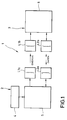
- the system for the transmission of data and energy designated in its entirety by reference number 1 in FIG. 1, comprises a main unit 2 and a secondary unit 3.
- the main unit 2 comprises a power supply unit 4 for supplying a main circuit device 5 which is provided with a first and a second Coupling element L1a, L2a is connected.
- the secondary unit 3 comprises a secondary circuit device 6, which is connected to a third and fourth coupling element L1b, L2b.
- An energy transmission from the main unit 2 to the secondary unit 3 takes place via the first and third coupling elements L1a, L1b.
- a bidirectional data transmission between the main unit 2 and the secondary unit 3 takes place via the second and fourth coupling elements L2a, L2b.
- the coupling elements L1a, L1b, L2a, L2b have the form of coils for generating an inductive coupling.
- the secondary unit 3 comprises a rectifier circuit 7, which converts the alternating supply signal received by the third coupling element L1b into a DC supply voltage V cc .
- the third coupling element L1b is also followed by a first signal shaping circuit 8, which converts the received, essentially sinusoidal signal into an essentially rectangular clock signal, which is supplied on the one hand to a reference counter 9 and on the other hand to a sequence control circuit 10.
- the fourth coupling element L2b is followed by a first transmit / receive changeover switch 11, the switching state of which is determined by the sequence control circuit 10.
- the first transmission / reception switch 11 connects the fourth coupling element L2b to a second signal shaping circuit 12, which is connected on the input side to a data counter 13.
- a microprocessor 14 is connected both to the reference counter 9 and to the data counter 13 and is also connected to the sequence control circuit 10 for mutual data exchange.
- the microprocessor 14 has a reset logic circuit 15, which resets the microprocessor, for example, when the supply voltage V cc is initially applied and in the event of undesired program states occurring.
- a frequency shift keying circuit 16 for the retransmission of data from the secondary unit 3 to the main unit 2 is controlled by the microprocessor 14 for binary frequency shift keying depending on the logical value of the bit to be retransmitted and is connected on the output side to the first transmission / reception switch 11, the frequency shift keying circuit 16 connects in its transmit position with the fourth coupling element L2b.
- the main unit 2 comprises a host computer 17 which is in communication with a second microprocessor 18.
- the main unit 2 further comprises an oscillator 19 which is connected to a power amplifier 20 which is connected on the output side to the first coupling element L1a for transmitting a high-frequency supply change signal to the secondary unit 3.
- the output signal of the oscillator 19 is supplied to the second coupling element L2a as a function of a gate time or switch-on time defined by the second microprocessor 18 in the transmission position of a second transmission / reception switch 21.
- a short or long gate time corresponds to the connection of the output signal of the oscillator 19 to the second coupling element L2a to the transmission of a first or second binary data value from the main unit 2 to the secondary unit 3.
- this connects the second coupling element L2a to a first phase-locked loop 22 and a second phase-locked loop 23, each on the output side are connected to the second microprocessor 18.
- the first phase-locked loop 22 is responsive to signals of the first frequency generated by the frequency shift keying circuit 16 of the slave unit 3, while the second phase-locked loop 22 is responsive to signals of the second frequency from the frequency shift keying circuit 16.
- the transmission method is explained in more detail below with reference to FIGS. 2 to 4.
- a clock signal is generated in the auxiliary unit 3 by the first signal shaping circuit 8, with which the reference counter 9 is clocked or incremented.
- the data counter 13 is counted up in accordance with the vibrations of the transmitted data signal, the sequence control circuit 10 having the reference counter 9 counted from the receipt of the data signal and thus from the start of the counting of the data counter 13.
- the reference counter 9 is used to define a time window with a time base defined by the clock signal.
- the microprocessor 14 effects a readout of the data counter 13 at this point in time.
- the first microprocessor 14 switches the first transmission / reception switch 11 in order to initiate a retransmission of data from the secondary unit 3 to the main unit 2.
- the frequency shift keying circuit 16 now generates a transmission signal with one of two transmission frequencies.
- the second microprocessor 18 of the main unit has switched the second transmission / reception switch 21 after completion of the data transmission to the secondary unit 3, so that either the first or the second phase-locked control circuit 22, 23 to that of the secondary unit 3 sent signal responds, which in turn is detected by the second microprocessor 18. This completes the data retransmission.
- a multi-bit data retransmission requires a corresponding multiple frequency shift keying with a suitable multiple phase-locked loop instead of a binary frequency shift keying.
- the method and system according to the invention enable a very low amount of circuitry on the side of the auxiliary unit 3, which, in addition to comparators and basic gates, can be implemented almost exclusively with flip-flops for realizing counters and dividers. This makes it easy to design the slave unit as a user-specific integrated circuit.
- both the main unit and the secondary unit can have the other unit wait before each data transmission in order to perform certain time-critical tasks.
- the method according to the invention is also characterized by a high level of transmission security.
- a suitable choice of the time window almost any transmission security can be achieved. If the time window defined in terms of circuitry is chosen large enough, the data counter contents can be interpreted by suitable software in such a way that bits are transmitted in pairs, for example, or that the data counter contents corresponds directly to one byte. Of course, this leads to a reduction in the transmission security that can be achieved.
- the data transmission from the slave unit to the main unit is also insensitive to interference due to the selected frequency shift keying modulation method.
- the slave unit can send back one bit after each bit received, the transmission of a byte in both data directions is possible almost simultaneously.
Landscapes
- Engineering & Computer Science (AREA)
- Computer Networks & Wireless Communication (AREA)
- Signal Processing (AREA)
- Artificial Intelligence (AREA)
- Computer Vision & Pattern Recognition (AREA)
- Physics & Mathematics (AREA)
- General Physics & Mathematics (AREA)
- Theoretical Computer Science (AREA)
- Bidirectional Digital Transmission (AREA)
- Near-Field Transmission Systems (AREA)
- Selective Calling Equipment (AREA)
- Synchronisation In Digital Transmission Systems (AREA)
Priority Applications (1)
| Application Number | Priority Date | Filing Date | Title |
|---|---|---|---|
| AT91910294T ATE99474T1 (de) | 1990-06-12 | 1991-06-05 | Verfahren und system zum uebertragen von energie und daten. |
Applications Claiming Priority (2)
| Application Number | Priority Date | Filing Date | Title |
|---|---|---|---|
| DE4018814A DE4018814A1 (de) | 1990-06-12 | 1990-06-12 | Verfahren und system zum uebertragen von energie und daten |
| DE4018814 | 1990-06-12 |
Publications (2)
| Publication Number | Publication Date |
|---|---|
| EP0533709A1 EP0533709A1 (de) | 1993-03-31 |
| EP0533709B1 true EP0533709B1 (de) | 1993-12-29 |
Family
ID=6408272
Family Applications (1)
| Application Number | Title | Priority Date | Filing Date |
|---|---|---|---|
| EP19910910294 Expired - Lifetime EP0533709B1 (de) | 1990-06-12 | 1991-06-05 | Verfahren und system zum übertragen von energie und daten |
Country Status (7)
| Country | Link |
|---|---|
| EP (1) | EP0533709B1 (enExample) |
| JP (1) | JPH05502147A (enExample) |
| KR (1) | KR960000146B1 (enExample) |
| AU (1) | AU640026B2 (enExample) |
| CA (1) | CA2084995A1 (enExample) |
| DE (2) | DE4018814A1 (enExample) |
| WO (1) | WO1991020135A1 (enExample) |
Cited By (1)
| Publication number | Priority date | Publication date | Assignee | Title |
|---|---|---|---|---|
| US7458453B2 (en) | 2003-06-27 | 2008-12-02 | Christian Bauer Gmbh + Co. | Disk clutch and method for operating same |
Families Citing this family (6)
| Publication number | Priority date | Publication date | Assignee | Title |
|---|---|---|---|---|
| DE19636031A1 (de) * | 1996-09-05 | 1998-03-12 | Varchmin J Uwe Prof Dr Ing | Power-Bus |
| US8363744B2 (en) | 2001-06-10 | 2013-01-29 | Aloft Media, Llc | Method and system for robust, secure, and high-efficiency voice and packet transmission over ad-hoc, mesh, and MIMO communication networks |
| DE10228060A1 (de) * | 2002-06-19 | 2004-01-15 | Robert Bosch Gmbh | Verfahren und Schaltungsanordnung zur Übertragung binärer Nutzdaten |
| DE10240671A1 (de) | 2002-09-04 | 2004-03-18 | Christian Bauer Gmbh + Co | Klopfsensor eines Verbrennungsmotors |
| AT512504B1 (de) * | 2012-03-22 | 2013-09-15 | Seibersdorf Labor Gmbh | Vorrichtung und Verfahren zur Bestimmung der Kapazität |
| CN110350943B (zh) * | 2018-09-28 | 2023-09-15 | 深圳市速腾聚创科技有限公司 | 带能量传输的无线通讯装置及带能量传输的无线通讯方法 |
Family Cites Families (14)
| Publication number | Priority date | Publication date | Assignee | Title |
|---|---|---|---|---|
| FR2290801A1 (fr) * | 1974-11-08 | 1976-06-04 | Thomson Csf | Poste d'emission-reception d'informations mises sous forme numerique et dispositif de liaison bilaterale comportant deux tels postes |
| JPS5732144A (en) * | 1980-08-06 | 1982-02-20 | Nippon Gakki Seizo Kk | Energy and/or data transmitter and receiver |
| AU1999983A (en) * | 1982-10-01 | 1984-04-05 | Sugar Research Limited | Load monitoring means |
| DE3336717A1 (de) * | 1983-10-08 | 1985-04-25 | Dai Nippon Printing Co., Ltd., Tokio/Tokyo | Verfahren und vorrichtung zur kontaktlosen, elektromagnetischen hin- und rueckuebertragung von steuerbefehlen und daten |
| JPS60171475A (ja) * | 1984-02-15 | 1985-09-04 | アイデンティフィケ−ション・デバイセス・インコ−ポレ−テッド | 識別システム |
| JPS61101885A (ja) * | 1984-10-24 | 1986-05-20 | Tdk Corp | Icカ−ド結合方式 |
| DE3447560A1 (de) * | 1984-12-21 | 1986-07-10 | Angewandte Digital Elektronik Gmbh, 2051 Brunstorf | Einrichtung zur beruehrungslosen signal- und energieuebertragung |
| GB8507281D0 (en) * | 1985-03-20 | 1985-04-24 | Emi Ltd | Data communications system |
| JPS61283981A (ja) * | 1985-06-11 | 1986-12-13 | Nippon Denzai Kogyo Kenkyusho:Kk | 集積回路カ−ド |
| DE3631477C3 (de) * | 1986-09-16 | 1995-01-26 | Siegfried Dipl Ing Schwarz | Netzwerk für die Steuer-, Meß- und Regeltechnik zur Daten- und Energie-Übertragung |
| NL8700861A (nl) * | 1987-04-13 | 1988-11-01 | Nedap Nv | Lees-, schrijfsysteem met miniatuur informatiedrager. |
| DE3714195A1 (de) * | 1987-04-29 | 1988-11-10 | Fraunhofer Ges Forschung | Verfahren zur beruehrungslosen energie- und datenuebertragung, sowie mechanisch und elektronisch kodiertes schloss |
| ATE108965T1 (de) * | 1987-12-09 | 1994-08-15 | Omron Tateisi Electronics Co | Induktives datenübertragungssystem. |
| JPH0732368B2 (ja) * | 1987-12-09 | 1995-04-10 | オムロン株式会社 | データ通信装置 |
-
1990
- 1990-06-12 DE DE4018814A patent/DE4018814A1/de active Granted
-
1991
- 1991-06-05 DE DE91910294T patent/DE59100782D1/de not_active Expired - Fee Related
- 1991-06-05 JP JP3509507A patent/JPH05502147A/ja active Pending
- 1991-06-05 WO PCT/DE1991/000480 patent/WO1991020135A1/de not_active Ceased
- 1991-06-05 KR KR1019920703164A patent/KR960000146B1/ko not_active Expired - Lifetime
- 1991-06-05 CA CA002084995A patent/CA2084995A1/en not_active Abandoned
- 1991-06-05 AU AU79719/91A patent/AU640026B2/en not_active Ceased
- 1991-06-05 EP EP19910910294 patent/EP0533709B1/de not_active Expired - Lifetime
Cited By (1)
| Publication number | Priority date | Publication date | Assignee | Title |
|---|---|---|---|---|
| US7458453B2 (en) | 2003-06-27 | 2008-12-02 | Christian Bauer Gmbh + Co. | Disk clutch and method for operating same |
Also Published As
| Publication number | Publication date |
|---|---|
| AU640026B2 (en) | 1993-08-12 |
| DE4018814A1 (de) | 1992-01-02 |
| AU7971991A (en) | 1992-01-07 |
| KR960000146B1 (ko) | 1996-01-03 |
| KR930701798A (ko) | 1993-06-12 |
| JPH05502147A (ja) | 1993-04-15 |
| EP0533709A1 (de) | 1993-03-31 |
| WO1991020135A1 (de) | 1991-12-26 |
| CA2084995A1 (en) | 1991-12-13 |
| DE4018814C2 (enExample) | 1993-02-04 |
| DE59100782D1 (de) | 1994-02-10 |
Similar Documents
| Publication | Publication Date | Title |
|---|---|---|
| DE3041134C2 (de) | Datenübertragungsanordnung zur Datenübertragung über eine Stromleitung | |
| DE3850753T2 (de) | Induktives Datenübertragungssystem. | |
| DE3687811T2 (de) | Adressgeneration fuer schaltungseinheiten. | |
| EP0191019B1 (de) | Einrichtung zum übertragen von binären daten zwischen einem mobilen datenträger und einer feststation | |
| DE3237405C2 (de) | Datenübertragungssystem | |
| DE3041945A1 (de) | Sender-empfaenger fuer mittels optischer fasern uebertragene daten | |
| DE2403098A1 (de) | System zum uebertragen spaltphasenmanchesterkodierter zweiwertiger datensignale | |
| DD269478A5 (de) | Elektronisches datenverarbeitungssystem | |
| EP0533709B1 (de) | Verfahren und system zum übertragen von energie und daten | |
| DE2449660C3 (de) | Verfahren und Einrichtung zur Synchronisation von im Zeitmultiplex arbeitenden, untereinander gleichberechtigten autonomen Geberstationen | |
| EP0150540B1 (de) | Verfahren zur Datenübertragung, sowie Station zur Durchführung des Verfahrens | |
| EP0559159B1 (de) | Elektronische Schliessanordnung | |
| DE69008917T2 (de) | Einrichtungen mit Frequenzumtastung für Stromschleife. | |
| DE2134783C3 (de) | Verfahren zur Ermittlung von Fehlern in den mit Regeneratoren versehenen Zwischenstellen eines mit Pulscodemodulation arbeitenden Übertragungssystems | |
| EP0715412B1 (de) | Verfahren und Anordnung zur Ermittlung von Phasenänderungen eines Referenz-Eingangssignals eines Phasenregelkreises | |
| DE1960790C3 (de) | Adreßcodiertes Übermittlungssystem nach dem Pulslage-Modulationsverfahren | |
| EP0079527B1 (de) | Datenübertragungsanlage für Vollduplexübertragung | |
| DE3421493A1 (de) | Datenuebertragungssystem | |
| DE2439246C3 (de) | Phasensynchronisierschaltung | |
| DE2818916C2 (de) | Einrichtung zum Synchronisieren mehrerer autonom im Zeitmultiplexbetrieb sendender Sendestationen | |
| DE2912854A1 (de) | Demodulationsverfahren fuer binaere frequenzmodulierte signale | |
| EP0433706B1 (de) | Zusatzsignalübertragung in einem Übertragungssystem für digitale Signale hoher Bitfolgefrequenz | |
| DE2513780C3 (de) | Phasensynchronisationsschaltung zur Regulierung des Gleichlaufs zwischen der Sende- und Empfangstrommel bei Faksimile-Geräten | |
| DE68905630T2 (de) | Verfahren und anordnung zur synchronisation von terminals, die ueber eine kette ohne zeittransparenz kommunizieren. | |
| DE2106172B2 (de) | Digitales synchronmodem |
Legal Events
| Date | Code | Title | Description |
|---|---|---|---|
| PUAI | Public reference made under article 153(3) epc to a published international application that has entered the european phase |
Free format text: ORIGINAL CODE: 0009012 |
|
| 17P | Request for examination filed |
Effective date: 19921113 |
|
| AK | Designated contracting states |
Kind code of ref document: A1 Designated state(s): AT BE CH DE DK ES FR GB GR IT LI LU NL SE |
|
| 17Q | First examination report despatched |
Effective date: 19930517 |
|
| GRAA | (expected) grant |
Free format text: ORIGINAL CODE: 0009210 |
|
| AK | Designated contracting states |
Kind code of ref document: B1 Designated state(s): AT BE CH DE DK ES FR GB GR IT LI LU NL SE |
|
| PG25 | Lapsed in a contracting state [announced via postgrant information from national office to epo] |
Ref country code: GR Free format text: LAPSE BECAUSE OF FAILURE TO SUBMIT A TRANSLATION OF THE DESCRIPTION OR TO PAY THE FEE WITHIN THE PRESCRIBED TIME-LIMIT Effective date: 19931229 Ref country code: SE Effective date: 19931229 Ref country code: NL Effective date: 19931229 Ref country code: ES Free format text: THE PATENT HAS BEEN ANNULLED BY A DECISION OF A NATIONAL AUTHORITY Effective date: 19931229 Ref country code: DK Effective date: 19931229 Ref country code: BE Effective date: 19931229 |
|
| REF | Corresponds to: |
Ref document number: 99474 Country of ref document: AT Date of ref document: 19940115 Kind code of ref document: T |
|
| ITF | It: translation for a ep patent filed | ||
| GBT | Gb: translation of ep patent filed (gb section 77(6)(a)/1977) |
Effective date: 19940111 |
|
| RIN2 | Information on inventor provided after grant (corrected) |
Free format text: KUEHN, JUERGEN * DALSASS, KARL-GUENTHER * SCHERER, KLAUS * VOLKWEIN, BERND |
|
| REF | Corresponds to: |
Ref document number: 59100782 Country of ref document: DE Date of ref document: 19940210 |
|
| ET | Fr: translation filed | ||
| PGFP | Annual fee paid to national office [announced via postgrant information from national office to epo] |
Ref country code: AT Payment date: 19940613 Year of fee payment: 4 |
|
| NLV1 | Nl: lapsed or annulled due to failure to fulfill the requirements of art. 29p and 29m of the patents act | ||
| PG25 | Lapsed in a contracting state [announced via postgrant information from national office to epo] |
Ref country code: LU Free format text: LAPSE BECAUSE OF NON-PAYMENT OF DUE FEES Effective date: 19940630 |
|
| PLBE | No opposition filed within time limit |
Free format text: ORIGINAL CODE: 0009261 |
|
| STAA | Information on the status of an ep patent application or granted ep patent |
Free format text: STATUS: NO OPPOSITION FILED WITHIN TIME LIMIT |
|
| 26N | No opposition filed | ||
| PG25 | Lapsed in a contracting state [announced via postgrant information from national office to epo] |
Ref country code: AT Effective date: 19950605 |
|
| PGFP | Annual fee paid to national office [announced via postgrant information from national office to epo] |
Ref country code: FR Payment date: 19960614 Year of fee payment: 6 |
|
| PGFP | Annual fee paid to national office [announced via postgrant information from national office to epo] |
Ref country code: CH Payment date: 19960621 Year of fee payment: 6 |
|
| PGFP | Annual fee paid to national office [announced via postgrant information from national office to epo] |
Ref country code: DE Payment date: 19960703 Year of fee payment: 6 |
|
| PGFP | Annual fee paid to national office [announced via postgrant information from national office to epo] |
Ref country code: GB Payment date: 19970527 Year of fee payment: 7 |
|
| PG25 | Lapsed in a contracting state [announced via postgrant information from national office to epo] |
Ref country code: LI Free format text: LAPSE BECAUSE OF NON-PAYMENT OF DUE FEES Effective date: 19970630 Ref country code: CH Free format text: LAPSE BECAUSE OF NON-PAYMENT OF DUE FEES Effective date: 19970630 |
|
| REG | Reference to a national code |
Ref country code: CH Ref legal event code: PL |
|
| PG25 | Lapsed in a contracting state [announced via postgrant information from national office to epo] |
Ref country code: FR Free format text: LAPSE BECAUSE OF NON-PAYMENT OF DUE FEES Effective date: 19980227 |
|
| PG25 | Lapsed in a contracting state [announced via postgrant information from national office to epo] |
Ref country code: DE Free format text: LAPSE BECAUSE OF NON-PAYMENT OF DUE FEES Effective date: 19980303 |
|
| REG | Reference to a national code |
Ref country code: FR Ref legal event code: ST |
|
| REG | Reference to a national code |
Ref country code: FR Ref legal event code: ST |
|
| PG25 | Lapsed in a contracting state [announced via postgrant information from national office to epo] |
Ref country code: GB Free format text: LAPSE BECAUSE OF NON-PAYMENT OF DUE FEES Effective date: 19980605 |
|
| GBPC | Gb: european patent ceased through non-payment of renewal fee |
Effective date: 19980605 |
|
| PG25 | Lapsed in a contracting state [announced via postgrant information from national office to epo] |
Ref country code: IT Free format text: LAPSE BECAUSE OF NON-PAYMENT OF DUE FEES;WARNING: LAPSES OF ITALIAN PATENTS WITH EFFECTIVE DATE BEFORE 2007 MAY HAVE OCCURRED AT ANY TIME BEFORE 2007. THE CORRECT EFFECTIVE DATE MAY BE DIFFERENT FROM THE ONE RECORDED. Effective date: 20050605 |