EP0521859B1 - Pll-frequenzsynthesierer mit hartem begrenzer gesteuert durch einen direkten digital-synthesierer - Google Patents
Pll-frequenzsynthesierer mit hartem begrenzer gesteuert durch einen direkten digital-synthesierer Download PDFInfo
- Publication number
- EP0521859B1 EP0521859B1 EP91903171A EP91903171A EP0521859B1 EP 0521859 B1 EP0521859 B1 EP 0521859B1 EP 91903171 A EP91903171 A EP 91903171A EP 91903171 A EP91903171 A EP 91903171A EP 0521859 B1 EP0521859 B1 EP 0521859B1
- Authority
- EP
- European Patent Office
- Prior art keywords
- output
- frequency
- signal
- dds
- loop
- Prior art date
- Legal status (The legal status is an assumption and is not a legal conclusion. Google has not performed a legal analysis and makes no representation as to the accuracy of the status listed.)
- Expired - Lifetime
Links
Images


Classifications
-
- H—ELECTRICITY
- H03—ELECTRONIC CIRCUITRY
- H03L—AUTOMATIC CONTROL, STARTING, SYNCHRONISATION, OR STABILISATION OF GENERATORS OF ELECTRONIC OSCILLATIONS OR PULSES
- H03L7/00—Automatic control of frequency or phase; Synchronisation
- H03L7/06—Automatic control of frequency or phase; Synchronisation using a reference signal applied to a frequency- or phase-locked loop
- H03L7/16—Indirect frequency synthesis, i.e. generating a desired one of a number of predetermined frequencies using a frequency- or phase-locked loop
- H03L7/18—Indirect frequency synthesis, i.e. generating a desired one of a number of predetermined frequencies using a frequency- or phase-locked loop using a frequency divider or counter in the loop
- H03L7/183—Indirect frequency synthesis, i.e. generating a desired one of a number of predetermined frequencies using a frequency- or phase-locked loop using a frequency divider or counter in the loop a time difference being used for locking the loop, the counter counting between fixed numbers or the frequency divider dividing by a fixed number
-
- H—ELECTRICITY
- H03—ELECTRONIC CIRCUITRY
- H03L—AUTOMATIC CONTROL, STARTING, SYNCHRONISATION, OR STABILISATION OF GENERATORS OF ELECTRONIC OSCILLATIONS OR PULSES
- H03L7/00—Automatic control of frequency or phase; Synchronisation
- H03L7/06—Automatic control of frequency or phase; Synchronisation using a reference signal applied to a frequency- or phase-locked loop
- H03L7/16—Indirect frequency synthesis, i.e. generating a desired one of a number of predetermined frequencies using a frequency- or phase-locked loop
- H03L7/18—Indirect frequency synthesis, i.e. generating a desired one of a number of predetermined frequencies using a frequency- or phase-locked loop using a frequency divider or counter in the loop
- H03L7/1806—Indirect frequency synthesis, i.e. generating a desired one of a number of predetermined frequencies using a frequency- or phase-locked loop using a frequency divider or counter in the loop the frequency divider comprising a phase accumulator generating the frequency divided signal
Definitions
- the present invention relates to frequency synthesizers. More specifically, the present invention relates to a novel and improved apparatus and method for frequency synthesis utilizing a direct digital synthesizer (DDS) capable of generating any one of a plurality of periodic reference signals, each having a different periodic frequency.
- DDS direct digital synthesizer
- phase lock loop is designed to output a signal at a range of frequencies with frequency resolution, or step size, equal to the loop reference frequency.
- phase lock loops synthesize a frequency by using a control voltage to drive a voltage controlled oscillator (VCO) which generates a signal of a frequency near the desired frequency.
- VCO voltage controlled oscillator
- a frequency divider is used to divide the VCO signal output frequency by an integer value. The integer value is chosen such that if the VCO were generating exactly the desired frequency, the resultant divided frequency signal would be exactly the same reference frequency.
- the divided frequency signal is input along with the reference frequency signal to a phase detector.
- the phase detector compares the phase of the two input signals and outputs a voltage proportional to the difference in phase of the two input signals.
- the output of the phase detector is coupled through a loop filter, necessary to insure loop stability, where it is input to the VCO as the control voltage. Accordingly, the output signal from the VCO is adjusted to a frequency exactly that of the desired frequency.
- the performance of a phase lock loop is related to several factors including (1) the frequency of the reference signal, (2) the magnitude of the divisor necessary to divide the output frequency down to the reference frequency, and (3) the bandwidth of the loop filter.
- the frequency of the reference signal dictates the frequency resolution, or step size of the loop, i.e. the smaller the reference frequency, the greater the frequency resolution.
- the magnitude of the loop divisor has great impact on the noise performance of the loop. As such, any phase noise or spurious noise in the reference frequency will appear in the loop output having its original magnitude multiplied by the loop divisor.
- the bandwidth of the loop filter which is normally five to ten percent of the reference frequency, impacts the speed with which the loop can settle on a new frequency. Thus the narrower the loop filter bandwidth, the slower the loop will be able to settle on the new frequency.
- Frequency synthesis may also be accomplished using a direct digital synthesizers (DDS).
- DDS can be utilized to provide a periodic signal variable in frequency over a bandwidth with fine frequency resolution.
- the DDS produces digitized periodic frequencies by accumulating phase at a higher rate consistent with sampling theory, translating the phase into a periodic waveform via a lookup table, and converting the resulting digital representation of the periodic wave to an analog signal using a digital to analog converter.
- the DDS output signal can contain amplitude modulated (AM) noise spurs due to quantizaton errors and thermal noise in the DDS. It is therefore desirable to eliminate these spurs from the DDS output signal.
- AM amplitude modulated
- DDS direct digital synthesizer
- Yet another object of the present invention is to provide a novel and improved phase lock loop frequency synthesizer which has substantially faster frequency switching time than a conventional frequency synthesizer of comparable frequency resolution and frequency range.
- the present invention is a novel and improved method and apparatus for synthesizing frequencies.
- the output of a direct digital synthesizer is provided, either directly or though a filter and/or a hard limiter to a phase lock loop.
- a DDS can be utilized to provide a periodic signal variable in frequency over a bandwidth with fine frequency resolution.
- the coupling of the output of the DDS to a phase lock loop provides one withthe capability to gererate a frequencies of fine resolution over a relatively large bandwidth.
- the DDS analog output signal may be provided directly to a filter, typically a bandpass filter, which eliminates the out of band noise spurs.
- the filtered output signal is then provided to a phase lock loop.
- the DDS output signal may contain amplitude modulated (AM) noise spurs due to quantizaton errors of the DDS.
- AM amplitude modulated
- the limiter limits the amplitude of the DDS output signal, spurious noise is eliminated except for higher uneven order harmonics of the generated fundamental frequency.
- the output of the limiter may be input to a filter, typically a bandpass filter, to eliminate the frequency harmonics.
- the output of the filter thus is a clean, analog signal at the desired fundamental frequency containing phase modulated (PM) spurious signals only.
- the DDS analog output signal may be provided directly to a filter, typically a bandpass filter, which eliminates the out of band noise spurs.
- the filtered output signal is then provided to the limiter which eliminates the spurs, except for the higher uneven order harmonics of the fundamental frequency, and phase modulated (PM) spurious signals.
- This type of signal may be characterized as containing the frequency components of a square wave. A signal of this type is particularly useful in digital circuits for uses such as clock signals.
- phase lock loop frequency synthesizer An implementation of the DDS with hard limiter and filter is illustrated in the form of a phase lock loop frequency synthesizer in which the DDS is used to provide a loop reference frequency to the phase lock loop.
- the DDS generated analog signal thus serves as a source for a reference frequency for the phase lock loop.
- the phase lock loop frequency synthesizer makes coarse output frequency adjustments, in increments of the nominal reference frequency, by varying the loop divisor value.
- the phase lock loop frequency synthesizer further makes fine output frequency adjustments by varying the DDS output frequency, e.g. the source of the phase lock loop reference frequency. Therefore, the fine adjustment increment is the frequency resolution of the DDS output multiplied by the value of the loop divisor.
- the phase lock loop can operate with a relatively high nominal reference frequency, thus allowing for a loop filter of relatively wide bandwidth. Accordingly the phase lock loop can operate with a relatively fast switching time.
- very fine output frequency step size changes may be realized because the step size is the loop divisor multiplied by the DDS frequency resolution. Such step size changes are typically several orders of magnitude finer than a conventional fine tune phase lock loop.
- a DDS driven phase lock loop frequency synthesizer with a hard limiter provides enhancements in output frequency resolution and clarity, at substantially faster switching speeds, over the prior art devices. Further, such a phase lock loop frequency synthesizer requires only one phase lock loop and one DDS. DDS's are typically VLSI devices and therefore require relatively little space or power. Thus, the hardware, space, and power requirements of the DDS driven phase lock loop frequency synthesizer are substantially less than that of a conventional multi-loop frequency synthesizer.
- the DDS driven phase lock loop frequency synthesizer also eliminates the wideband spurious noise associated with the mixing of outputs from multiple phase lock loops, because the present invention requires no such mixing.
- the DDS driven phase lock loop frequency synthesizer further suppresses and eliminates spurious noise by coupling a DDS "clean-up" filter between the DDS output and the phase detector input of the phase lock loop.
- the DDS "clean-up” filter is fundamental to this invention. This filter suppresses and eliminates wideband spurs from the DDS reference signal before the phase lock loop multiplies the magnitude of the spurs.
- the phase lock loop multiplies the magnitude of the DDS spurs, not the relative frequency.
- the output of the phase lock loop will contain DDS spurious tones within ⁇ B/2 of the output frequency, f out where B is the bandwidth of the "clean-up" filter. Spurious signals will be suppressed beyond fout ⁇ B/2. This principle is ideal in situations where the synthesizer output is to be modulated, since the dose-in DDS spurs can be hidden in the modulated spectrum.
- a high order "clean-up" filter with sharp cutoffs can be physically realized more easily at certain frequencies. These frequencies are typically much higher than the desired phase lock loop reference frequency. This allows for the effective placement of the "clean-up" filter center frequency, while still providing the loop with an appropriate reference frequency.
- the nominal output of the DDS is set at a frequency at which a good "clean-up" filter can be realized.
- a fixed value frequency divider may be positioned between the output of the "clean-up" filter and the reference input to the phase lock loop. This frequency divider divides the filtered DDS output signal down in frequency to an appropriate reference frequency for the phase lock loop. It is known that a frequency divider has the property of lowering spurious phase noise by a factor of its divisor value. Therefore the frequency divider further suppresses any narrow band spurious noise which passes through the "clean-up" filter.
- the preferred embodiments of the present invention therefore provide several advantages and improvements over prior art frequency synthesizers. These improvements include finer output frequency resolution, cleaner output signal frequency, flexibility in waveform generation, faster switching time, a reduction in hardware, space, and power requirements, and improved noise characteristics.
- Prior art frequency synthesizers typically utilize multiple phase lock loops to obtain frequency resolution and cover the desired bandwidth.
- Such multi-loop designs usually incorporate frequency mixers to combine the outputs of the loops. It is well known that such mixers inherently introduce spurious intermodulation products. Many broadband spurs are typically generated, as opposed to the dose in and readily predictable spurs created by a direct digital synthesizer.
- DDS direct digital synthesizer
- a hard limiter i.e., an amplitude limiter
- the use of a limiter is found to significantly reduce spurious noise in the DDS generated analog signal.
- the noise which the limiter removes is essentially an amplitude modulated (AM) noise.
- AM noise is quantization spurious emissions due to the digital to analog converter (DAC) in the DDS.
- DAC digital to analog converter
- the DDS also generates phase modulated (PM) noise. Both the the AM and PM noise affect the frequency purity of the DDS output signal.
- FIG. 1 illustrates such an exemplary embodiment of a frequency synthesizer wherein the DDS drives, through a filter and limiter, a phase lock loop.
- frequency synthesizer 100 is configured with direct digital synthesizer (DDS) 102 driving a phase lock loop.
- DDS 102 serves as a variable reference source means for generating a selected one of a plurality of reference frequency signals, each at a different frequency.
- DDS 102 typically comprises phase accumulator 104, sine lookup table 106 and digital to analog converter (DAC) 108.
- Phase accumulator 104 receives a digital fine frequency control signal which determines the phase increment for accumulation at the DDS dock rate.
- the accumulated phase value is output to sine lookup table 106, typically a read only memory which stores sine values.
- Sine lookup table 106 provides an output signal, indicative of the digital representation of a periodic waveform, as an input to DAC 108.
- DAC 108 converts the digital representation of the periodic waveform into an analog amplitude value as the output reference signal which is an analog representation of the periodic waveform.
- DDS 102 is responsive to the fine frequency control signal for altering the frequency of the output reference signal.
- DDS 102 is further responsive to a direct digital synthesizer clock signal with which its internal digital hardware is driven.
- the output from DDS 102, specifically DAC 108, is provided to an input of direct digital synthesizer "clean-up" filter 110.
- Filter 110 serves as a filter means for enhancing the spectral purity of the reference signal output from DAC 108.
- the enhanced reference signal output from filter 110 is coupled as an input to limiter 111.
- Limiter 111 is conventionally referred to as a "hard” limiter in that it limits the maximum amplitude of the filtered reference signal to a predetermined level.
- the output of limiter 111 is provided as a limited/enhanced reference signal to an input of optional frequency divider 112. Should divider 112 not be used, the output of limiter 111 is provided as an input to phase lock loop 114, and more particularly as an input to phase detector 116.
- Limiter 111 may be constructed in many different forms.
- One simple form is that of back-to-back diodes.
- Another form of a limiter is that of a saturating amplifier, such as the case of an op amp voltage comparator.
- Another form in which the limiter may be is that of an inverter logic gate having the output coupled to the input through a resistor of such a value as 100 K ⁇ .
- Limiter 111 is utilized to suppress the amplitude modulated (AM) spurious components from the DDS generated signal.
- the spurious components are the AM portion of the amplitude quantization process, as well as the AM portion of the thermal noise.
- the use of the limiter facilitates elimination of these AM spurs.
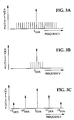
- Figures 3A-3C are provided.
- Figures 3A-3C are an illustration of the frequency spectrum of the signals as output from DDS 102 through filter 110 and limiter 111 at various points in the circuit of Figure 1.
- Figure 3A corresponds to the frequency spectrum of the signal output from DDS 102 to filter 110 at point A of Figure 1.
- Figures 3B and 3C respectively correspond to the signals at points B and C as respective outputs from filter 110 and limiter 111 of Figure 1.
- the AM spurs are illustrated as a function of amplitude with respect to frequency.
- the output of the DDS at point A is characterized as a strong signal at the fundamental frequency, f DDS , surrounded by much weaker spurious signals at various frequencies.
- the output of the bandpass filter at point B is characterized again as a strong signal at the fundamental frequency, f DDS , but surrounded by much weaker spurious signals only within the pass band of the filter. Hence the filter eliminates all spurs at out of band frequencies.
- the output of the limiter at point C is characterized again as a strong signal at the fundamental frequency.
- limiter 111 is removed from between the output of filter 110 and the input of divider 112, and inserted between the output of DAC 108 and the input of filter 110.
- the limiter is illustrated in Figure 1 in dashed lines and identified by the reference numeral 111'. Accordingly, the signal output from DDS 102 is limited in amplitude and provided to an input of filter 110.
- Filter 110 filters undesirable frequency components from the amplitude limited reference signal.
- the limited/enhanced reference signal as output from filter 102 is provided as an input to divider 112. Should divider 112 not be used, the output of filter 110 is provided as an input to phase lock loop 114, and more particularly as an input to phase detector 116.
- Figures 4A-4C are provided.
- Figures 4A-4C are an illustration of the frequency spectrum of the signals as output from DDS 102 through limiter 111' and filter 110 is provided for various points in the circuit of Figure 1.
- Figure 4A corresponds to the frequency spectrum of the signal output from DDS 102 to limiter 111' at point A of Figure 1.
- Figures 4B and 4C respectively correspond to the signals at points B' and C' as respective outputs from limiter 111' and filter 110 of Figure 1.
- the AM spurs are illustrated as a function of amplitude with respect to frequency.
- the output of the DDS at point A is characterized as a strong signal at the fundamental frequency, f DDS , surrounded by much weaker spurious signals at various frequencies as was for Figure 3A.
- the output of the limiter at point B' is characterized again as a strong signal at the fundamental frequency, f DDS , with substantially all spurious signals eliminated with the exception of signals at the higher uneven order harmonics of the fundamental frequency, i.e. ⁇ 3f DDS , ⁇ 5f DDS , etc.
- divider 112 serves as a reference signal divider means for generating a divided reference signal having a periodic frequency equal to the frequency of the limited/enhanced reference signal divided by a predetermined integer value, M.
- the frequency divided reference signal is provided to phase lock loop 114 as the phase lock loop reference frequency.
- phase lock loop 114 is comprised of phase detector 116, loop filter 118, voltage controlled oscillator (VCO) 120 and loop divider 122.
- Phase lock loop 114 serves as a frequency tuning means for generating a loop output signal having a periodic frequency which is an integer multiple of the frequency of the input reference signal.
- phase detector 116 is coupled to the output of limiter 111, or divider 112 if provided.
- limiter 111' positioned at the output of DDS 102
- the output of filter 110,or divider 112 if provided is coupled to on input of phase detector 116.
- the output of phase detector 116 is coupled to an input of loop filter 118, typically constructed as an op amp filter.
- the output of loop filter 118 is coupled to a control input of VCO 120.
- the output of VCO 120 is provided as the phase lock loop output signal and is also fed back to an input of loop divider 122.
- the output of loop divider 122 is coupled as the other input of phase detector 116.
- Phase detector 116 serves as a comparator means for comparing the DDS circuitry provided reference signal to the divided loop output signal. Phase detector 116 is responsive to a difference in phase of the reference signal from the DDS circuitry and the divided loop output signal for generating a frequency tuning control signal. Phase detector 116 generates the frequency tuning control signal whose voltage level is proportional to the difference in frequencies of the compared signals.
- Loop filter 118 serves as a tuning control signal filter. Loop filter 118 receives and filters the frequency tuning control signal and provides a VCO control signal. The VCO control signal is provided to the voltage control input of VCO 120.
- VCO 120 serves as a frequency generation means for generating the loop output signal in response to the VCO control signal. Specifically, VCO 120 alters the frequency of the loop output signal in response to a change in the voltage level of the input VCO control signal.
- Loop divider 122 is coupled to the output of VCO 120 so as to receive the loop output signal.
- Loop divider 122 serves as a loop divider means which receives the loop output signal and generates a divided loop signal which corresponds in frequency to the loop output signal divided by N.
- the divided loop signal is provided to the other input of phase comparator 116.
- Loop divider 122 is responsive to a coarse frequency control signal for setting the integer divisor value by which the loop output signal frequency is divided for feedback to phase detector 116.
- the DDS produces digitized periodic waveforms, typically a sine wave although a square wave may as easily be generated, of a given frequency by accumulating phase at a higher rate.
- the accumulated phase is translated to a periodic waveform via a lookup table.
- the resulting digital representation of the periodic waveform is translated to analog form using a digital to analog converter.
- Phase lock loop 114 is designed to output a range of frequencies where the frequency resolution is equal to its reference frequency.
- phase lock loop 114 is designed for loop output signals that can vary from 200-400 MHz. If the reference frequency applied to phase lock loop 114 is 10 MHz, the possible outputs from phase lock loop 114 are 200, 210, 220, 230,...., 390, and 400 MHz.
- the frequency of each phase lock loop output signal is the division ratio of the loop, the value by which output divider 122 divides, multiplied by the reference frequency.
- the reference frequency may be made to vary in extremely small steps. Note that the step size of the DDS driven phase lock loop varies with the divisor value of the loop divider (N) and is therefore not constant throughout the range of output frequencies.
- Filter 110 is a critical component and is preferably a bandpass filter designed with as narrow a bandwidth and as steep a roll-off as possible. This filter may therefore be a crystal filter or a surface acoustic wave (SAW) filter.
- SAW surface acoustic wave
- Use of the optional divider 112 provides versatility in selection of the center frequency of filter 110. For example, it is sometimes difficult to obtain a crystal filter with a center frequency of 1 MHz, but straightforward to specify a center frequency of 10 MHz. A design which requires a reference frequency to phase lock loop 114 of 1 MHz can therefore be realized. Accordingly, a DDS output signal with its frequency centered at 10 MHz, is provided as an input to a 10 MHz crystal filter.
- the output of the crystal filter is provided to a fixed divide by 10 divider before being applied at the phase lock loop input.
- Divider 112 has the added benefit of reducing the amplitude of the DDS phase noise and spurious content by 20log(M) dB, where M is the fixed division ratio.
- the spurious performance of the frequency synthesizer of Figure 1 may be readily analyzed.
- the DDS output includes spurious signals typically caused by phase truncation of the output waveform, amplitude quantization of the waveform, nonlinearities of the DAC output, and aliases attributable to the sampling process.
- the phase noise in the DDS output is governed by the phase noise characteristics of the DDS clock signal, as well as the noise performance of the digital circuitry comprising the DDS. As was discussed earlier with reference to Figures 3A-3C and 4A-4C, many of the noise spurs may be significantly reduced or eliminated.
- Phase lock loop 114 acts as a low pass filter to signals applied to its reference input.
- the loop has second order low pass filter characteristics with a bandwidth equal to the phase lock loop bandwidth.
- Reference spurs and phase noise are multiplied in the loop by the factor N in voltage or 20log(N) in dB, where N is the divisor value of loop divider 122.
- the loop output signal is therefore characterized by the output frequency surrounded by a bandpass spectrum of multiplied reference spurs and phase noise.
- this spectrum is the spurious content of the DDS output plus 20log(M) dB, and suppressed by 6 dB per octave outside of the phase lock loop bandwidth.
- Filter 110 is utilized to provide suppression of spurious signals and phase noise, particularly those generated by the DDS.
- phase lock loop multiplies the amplitude of the DDS spurious signals by N.
- the frequency difference between the phase lock loop synthesizer output frequency and the spur remains the same as that between the DDS output frequency and the DDS spur frequency.
- an FM modulation of the phase lock loop synthesizer output may occur. This modulation produces a family of spurs harmonically related to the DDS spur, decreasing in amplitude with the order of the harmonic.
- These FM spurs remain close in to the synthesizer output frequency and in general fall off rapidly. Therefore, spurs may be present at the synthesizer output within a bandwidth equal to that of filter 110 surrounding the output frequency. But beyond this the output can be made arbitrarily clean by selecting a filter 110 with a sufficient shape factor and ultimate attenuation.
- the use of filter 110 and limiter 111 serves to reduce the overall spurs generated by DDS 102.
- phase lock loop 114 has a 1 MHz step resolution.
- the reference input to phase lock loop 114 is centered at 1 MHz, and the value of the divisor of loop divider 122, N, is in the range 200 ⁇ N ⁇ 400.
- the output of the synthesizer is in steps of N times the reference frequency input to the phase lock loop from the DDS and filter/limiter arrangement.
- the DDS must output a range of frequencies sufficient to bridge the 1 MHz phase lock loop resolution.
- the bandwidth of the output of the DDS is therefore the loop frequency resolution divided by the minimum value of N, e.g. 1 MHz/200 which equals 5 KHz.
- the DDS must therefore output a signal at 1 MHz ⁇ 2.5 KHz.
- the resolution of the synthesizer is that of the DDS times N. With a typical DDS frequency resolution of 0.01 Hz, the synthesizer resolution varies from 2 Hz at the low frequency end to 4 Hz at the high frequency end. Ignoring transient response issues, filter 110 can be made as narrow as possible, i.e. approximately 6 KHz, 1 dB bandwidth. The synthesizer will output spurious signals attributable to the DDS within ⁇ 3KHz of the output tone, and falling off per the characteristic of filter 110, the characteristic of limiter 111, plus the loop response.
- the maximum level of these spurious signals in dB is the maximum level of the DDS spurs within the clean-up filter bandwidth plus 52 dB, where 52 dB is 10log(N max ), i.e., 10log(400).
- DDS phase noise is multiplied by 52 dB maximum, and is filtered both by filter 110 and the loop response.
- the synthesizer therefore produces close in spurious signals and a close in phase noise pedestal due to the reference, but no theoretical spurs far beyond the clean-up filter and loop bandwidth.
- the transient response and switching time of the frequency synthesizer of Figure 1 is established by the bandwidth of filter 110 and the loop characteristics of phase lock loop 114.
- a DDS has switching times typically less than 100 nsec, and therefore does not significantly effect the switching time.
- the settling time of a phase lock loop is inversely related to the loop bandwidth.
- the loop bandwidth of a phase lock loop can typically be no wider than five to ten percent of the frequency step size.
- the design of the frequency synthesizer of Figure 1 provides remarkably fine frequency resolution with a phase lock loop having a relatively large frequency step size, and therefore a wide permissible loop bandwidth.
- the phase lock loop of the the embodiment of Figure 1 will settle very quickly.
- switching time will be governed by the transient characteristic of filter 110, rather than the loop bandwidth of phase lock loop 114.
- the selection of filter 110 is a tradeoff between the spurious noise performance and switching speed of the synthesizer.
- DDS 102 and filter 110 could have been centered at 10 MHz and followed by divider 112 with a divisor value of 10. This circuitry would provide the 1 MHz ⁇ 2.5 KHz input to phase lock loop 114.
- the bandwidth of the filter 110 at 10 MHz would be approximately 60 KHz, providing faster settling time than the 6 KHz design. While the wider bandwidth clean-up filter passes a greater range of DDS spurs and noise, this is offset somewhat by the 20 dB improvement afforded by divider 112.
- FIG. 2 illustrates in block diagram form a frequency synthesizer which incorporates a DDS within the phase lock loop.
- synthesizer 200 includes circuit 202 which comprises a phase lock loop incorporating within the loop a direct digital synthesizer.
- Circuit 202 receives a reference frequency, typically from a frequency standard 204, through fixed reference divider 206. The frequency of the frequency standard output signal is divided by fixed reference divider 206 for input to circuit 202.
- Circuit 202 comprises phase detector 208, loop filter 210, VCO 212, optional loop divider 214, DDS 216, DDS cleanup filter 218, limiter 219 and optional loop divider 220.
- the output from fixed reference divider 206, f r is provided as one input to phase detector 208.
- the output of phase detector 208 is coupled as previously discussed to the input of loop filter 210.
- the output of loop filter 210 is coupled as the control voltage to VCO 212.
- VCO 212 is provided as the frequency synthesizer output with the VCO output signal also fed back either directly or through optional loop divider 214 to the DDS clock input of DDS 216.
- DDS 216 is provided with a frequency control input signal which is used to set the DDS frequency.
- the output of DDS 216 is to provided to filter 218.
- the output of filter 218 is provided to the input of limiter 219.
- the output of limiter 219 is provided either directly to or through optional loop divider 220 to the other input of phase detector 208.
- limiter 219 may be removed from the output of filter 218 and inserted at the input thereof. In this variation of Figure 2, the limiter is illustrated by the dashed lines indicated by the reference numeral 219'.
- the synthesizer output frequency is a function of the reference frequency f r , input to phase detector 208 from fixed reference divider 206; the number of bits in the digital word of the frequency control signal which controls DDS 216, N; the DDS step size determined by the frequency control signal, A; and the values of the dividers 214 and 220, respectively X and Y.
- each frequency synthesizer provides an output signal to a switching device, such as an FET transistor or PIN diode switch.
- a switching device such as an FET transistor or PIN diode switch.
- Such a switching device would provide selection between the outputs of the multiple frequency synthesizer for an ultimate output signal.
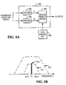
- FIG. 5A illustrates in block diagram form an exemplary application of the DDS driven phase lock loop described herein.
- upconverter 500 is comprised of low pass filters 502 and 504, and image reject mixer 506.
- I and Q channel baseband data or video signals are respectfully input to filters 502 and 504.
- the filtered I and Q channel signals are output from filters 502 and 504 to image reject mixer 506.
- DDS driven phase lock loop 508 generates a local oscillator signal for input to image reject mixer 506 of upconverter 500 where the input signals are upconverted in frequency
- the frequency upconverted signals are output from image reject mixer 506.
- the DDS driven phase lock loop generated signal appears spur-free when used to upconvert a relatively wide data or video spectrum.
- the frequency upconverted data or video spectrum envelope is illustrated by the dashed line 510.
- the carrier frequency f c is indicated by the reference numeral 512.
- the envelope of potential spurious tones is indicated by the dashed line 514.
Claims (24)
- Eine Frequenzsynthetisiervorrichtung, die folgendes aufweist:eine direkte digitale Synthetisiervorrichtung (DDS) mit einem Feinfrequenzsteuereingang und einem DDS Takt- oder Clock-Eingang zum jeweiligen Empfang von extern erzeugten Phasendaten und einem extern erzeugten Takt- oder Clocksignal und mit einem Ausgang, an dem ein Referenz- oder Bezugssignal vorgesehen wird, wobei die Direktdigitalsynthetisiervorrichtung folgendes aufweist:einen Phasenakkumulator mit einem Phasendateneingang zum Empfang der Phasendaten, einen Akkumulator-Takteingang zum Empfang des Takt- oder Clocksignals und einen Akkumulatorausgang;einen Nur-Lese-Speicher (ROM) mit einer Vielzahl von adressierbaren Speicherstellen oder -plätzen, deren jeder einen vorbestimmten Sinuswert speichert, einen Adresseneingang gekoppelt mit dem Akkumulatorausgang, einen Speichertakt- oder Clock-Eingang zum Empfang des Takt- oder Clocksignals und einen Speicherausgang; undeinen Digital-zu-Analogumwandler mit einem Umwandlereingang gekoppelt mit dem Speicherausgang, einen Konvertertakteingang zum Empfang des Takt- oder Clocksignals und einen Konverterausgang als den erwähnten DDS-Ausgang; undeinen Begrenzer mit einem Eingang gekoppelt mit dem Bezugssignal und einem Begrenzerausgang.
- Frequenzsynthetisiervorrichtung nach Anspruch 1, wobei ferner folgendes vorgesehen ist:
ein Filter mit einem Eingang gekoppelt mit dem Begrenzerausgang und einem Filterausgang. - Frequenzsynthetisiervorrichtung nach Anspruch 1, wobei ferner folgendes vorgesehen ist:
ein Filter angeordnet zwischen dem Digital-zu-Analogumwandler und dem Begrenzer mit einem Eingang gekoppelt mit dem Umwandler oder Konverterausgang und einem Filterausgang gekoppelt mit dem Begrenzereingang. - Frequenzsynthetisiervorrichtung nach Anspruch 3, wobei ferner folgendes vorgesehen ist:
ein Frequenzteiler mit einem Eingang gekoppelt mit dem Begrenzerausgang und einen Frequenzteilerausgang, wobei der Frequenzteiler die Bezugssignalfrequenz durch M teilt. - Frequenzsynthetisierer nach Anspruch 2, wobei ferner folgendes vorgesehen ist:
ein Frequenzteiler mit einem Eingang gekoppelt mit dem Filterausgang und einem Frequenzteilerausgang, wobei der Frequenzteiler die Referenz- oder Bezugssignalfrequenz durch M teilt. - Frequenzsynthetisiervorrichtung nach Anspruch 2, wobei ferner folgendes vorgesehen ist:
eine Phasenverriegelungsschleife mit einem Schleifeneingang gekoppelt mit dem Filterausgang, einen Grobfrequenzsteuereingang zum Empfang eines dividiert-durch-N-Signals, einen Schleifenausgang, wobei die Phasenverriegelungsschleife an dem Schleifenausgang ein Synthetisiervorrichtungsausgangssignal vorsieht, und zwar mit einer Frequenz, die N-mal die Frequenz des Bezugssignals ist. - Frequenzsynthetisiervorrichtung nach Anspruch 3, wobei ferner eine Phasenverriegelungsschleife vorgesehen ist, und zwar mit einem Schleifeneingang gekoppelt mit dem Begrenzerausgang, eine Grobfrequenzsteuerungseingangsgröße oder ein Grobfrequenzsteuerungseingang zum Empfang des dividiert-durch-N-Signals und eine Schleifenausgangsgröße oder ein Schleifenausgang, wobei die Phasenverriegelungsschleife an dem Schleifenausgang ein Synthetisiervorrichtungsausgangssignal erzeugt, und zwar mit einer Frequenz, die N-mal die Frequenz des Bezugssignals ist.
- Frequenzsynthetisiervorrichtung nach Anspruch 7, wobei ferner ein Frequenzteiler vorgesehen ist, und zwar angeordnet zwischen dem Begrenzer und der Phasenverriegelungsschleife, und zwar mit einem Eingang gekoppelt mit dem Begrenzerausgang und einen Frequenzteilerausgang gekoppelt mit dem Schleifeneingang, wobei der Frequenzteiler die Referenzsignalfrequenz durch M teilt, wobei die Phasenverriegelungsschleife das Synthetisiervorrichtungsausgangsgrößensignal mit einer Frequenz vorsieht, die N-mal größer ist als die Referenz-Signalfrequenz dividiert durch M.
- Frequenzsynthetisiervorrichtung nach Anspruch 6, wobei ferner folgendes vorgesehen ist:
ein Frequenzteiler angeordnet zwischen dem Filter und der Phasenverriegelungsschleife mit einem Eingang gekoppelt mit dem Filterausgang und ein Frequenzteilerausgang gekoppelt mit dem Schleifeneingang, wobei der Frequenzteiler die Bezugssignalfrequenz durch M teilt, wobei die Phasenverriegelungsschleife das Synthetisiervorrichtungsausgangssignal mit einer Frequenz vorsieht, die N-mal die Bezugssignalfrequenz dividiert durch M ist. - Frequenzsynthetisierer nach Anspruch 6, wobei die Phasenverriegelungsschleife folgendes aufweist:einen Phasendetektor mit einem Bezugsgrößeneingang gekoppelt mit dem Filterausgang, einen Rückkoppeleingang und einen Detektorausgang;ein Schleifenfilter mit einem Schleifenfiltereingang gekoppelt mit dem Detektorausgang, und einen Schleifenfilterausgang;einen spannungsgesteuerten Oszillator mit einem Steuereingang gekoppelt mit dem Schleifenfilterausgang und einen Oszillatorausgang, wobei das Synthetisiervorrichtungsausgangssignal an dem Oszillatorausgang vorgesehen wird; undeinen variablen Frequenzteiler mit einem Teilereingang gekoppelt mit dem Oszillatorausgang, einen Teilersteuereingang zum Empfang des dividiere durch N-Signals und einen Teilerausgang gekoppelt mit dem Detektorrückkopplungseingang.
- Frequenzsynthetisiervorrichtung nach Anspruch 7, wobei die Phasenverriegelungsschleife folgendes aufweist:einen Phasendetektor mit einem Bezugseingang gekoppelt mit dem Begrenzerausgang, einen Rückkoppeleingang und einen Detektorausgang;ein Schleifenfilter mit einem Schleifenfiltereingang gekoppelt mit dem Detektorausgang und einen Schleifenfilterausgang;einen spannungsgesteuerten Oszillator mit einem Steuereingang gekoppelt mit dem Schleifenfilterausgang und einen Oszillatorausgang, wobei das Synthetisiervorrichtungsausgangssignal an dem Oszillatorausgang vorgesehen wird; undeinen variablen Frequenzteiler mit einem Teilereingang gekoppelt mit dem Oszillatorausgang wobei ein Teilersteuereingang vorgesehen ist zum Empfang des Dividiere-durch-N-Signals und ein Teilerausgang gekoppelt mit dem Detektorrückkopplungseingang
- Frequenzsynthetisiervorrichtung nach Anspruch 8 wobei die Phasenverriegelungsschleife folgendes aufweist:Ein Phasendetektor mit einem Bezugsgrößeneingang gekoppelt mit dem Frequenzteilerausgang, einem Rückkopplungseingang und einem Detektorausgang;einen Schleifenfilter mit einem Schleifenfiltereingang gekoppelt mit dem Detektorausgang und einem Schleifenfilterausgang;einen spannungsgesteuerten Oszillator mit einem Steuereingang gekoppelt mit dem Schleifenfilterausgang und einem Oszillatorausgang wobei das Synthesisiervorrichtungsausgangssignal an dem Oszillatorausgang vorgesehen ist;und einem variablen Frequenzteiler mit einem Teilereingang gekoppelt mit dem Oszillatorausgang, einem Teilersteuereingang zum Empfang des Teile-durch-N-Signals und einen Teilerausgang gekoppelt mit dem Detektorrückkopplungseingang
- Frequenzsynthetisiervorrichtung nach Anspruch 9 wobei die Phasenverriegelungsschleife folgendes aufweist:ein Phasendetektor mit einem Bezugsgrößeneingang gekoppelt mit dem Frequenzteilerausgang, einem Rückkopplungseingang und einem Detektorausgang;ein Schleifenfilter mit einem Schleifenfiltereingang gekoppelt mit dem Detektorausgang und einem Schleifenfilterausgang;einen spannungsgesteuerten Oszillator mit einem Steuereingang gekoppelt mit dem Schleifenfilterausgang und einem Oszillatorausgang wobei das Synthetisiervorrichtungsausgangssignal an dem Oszialltorausgang vorgesehen ist;einen variablen Frequenzteiler mit einem Teilereingang gekoppelt mit dem Oszillatorausgang wobei der Teilersteuereingang zum Empfang des Teile-durch-N-Signals dient und wobei ein Teilerausgang mit dem Detektorrückkoppeleingang gekoppelt ist
- Frequenzsynthetisiervorrichtung nach Anspruch 2 wobei die Phasenverriegelungsschleife folgendes aufweist:ein Phasendetektor mit einem Bezugseingang zum Empfang eines extern erzeugten Frequenzstandardsignals mit einer vorbestimmten Frequenz, ein Rückkopplungseingang gekoppelt mit dem Filterausgang und ein Detektorausgang;ein Schleifenfilter mit einem Schleifenfiltereingang gekoppelt mit dem Detektorausgang und einem Schleifenfilterausgang;und einen spannungsgesteuerten Oszillator mit einem Steuereingang gekoppelt mit dem Schleifenfilterausgang und einem Oszillatorausgang wobei das Synthetisiervorrichtungsausgangssignal vorgesehen wird an dem Oszillatorausgang wobei der Oszillatorausgang mit dem DDS-Takteingang gekoppelt ist
- Frequenzsynthetisiervorrichtung nach Anspruch 3 wobei die Phasenverriegelungsschleifenvorrichtung folgendes aufweist:ein Phasendetektor mit einem Referenz eingang zum Empfang eines extern erzeugten Frequenzstandardsignals einer vorbestimmten Frequenz, ein Rückkopplungseingang gekoppelt mit dem Begrenzungsvorrichtungsausgang und ein Detektorausgang;ein Schleifenfilter mit einem Schleifenfiltereingang gekoppelt mit dem Detektorausgang und einem Schleifenfilterausgang; undeinen spannungsgesteuerten Oszillator mit einem Steuereingang gekoppelt mit dem Schleifenfilterausgang und einem Oszillatorausgang wobei das Synthetisiervorrichtungsausgangssignal an dem Oszillatorausgang vorgesehen ist und wobei der Oszillatorausgang mit dem DDS-Takt gekoppelt ist
- ein Verfahren zur Frequenzsynthetisierung wobei die folgenden Schritte vorgesehen sind:Vorsehen eines Direktsignalssynthetisierers DDS der in der Lage ist, ein DDS-Analogausgangssignal zu erzeugen und zwar bei einer Frequenz ausgewählt aus einer Vielzahl von Frequenzen;Vorsehen von extern erzeugten Phasendaten und Taktsignalen für den DDS;Erzeugung des DDS ansprechend auf eine Eingangsgröße oder einen Eingang der Phasendaten und des Taktsignals wobei das DDS-Analogausgangssignal eine Frequenz besitzt die den Phasendaten entspricht, wobei der Schritt des Erzeugens des DDS-Analogausgangssignals die folgenden Schritte aufweist:Akkumulieren von Phaseninkrementwerten der Phasendaten mit einer Rate entsprechend dem Taktsignal;Vorsehen eines akkumulierten Phaseninkrementwertausgangssignals entsprechend den akkumulierten Phaseninkrementwerten;Speichern einer Vielzahl von Amplitudenwerten deren jeder einem entsprechenden akkumulierten Phaseninkrementwert entspricht;Vorsehen eines Speicherausgangssignals welches eine Anzeige bildet für den Amplitudenwert entsprechend jedem akkumulierten Phaseninkrementwert des akkumulierten Phaseninkrementwertausgangssignals;Umwandeln des Speicherausgangssignals in ein Analogsignal entsprechend einem Amplitudenwert representiert durch das Speicherausgangssignal;Vorsehen des Analogsignals mit einer Rate entsprechend dem Taktsignal und zwar als das DDS-Analogausgangssignal; undBegrenzen der Amplitude des DDS-Analogausgangssignals
- Verfahren nach Anspruch 16 wobei ferner der Schritt des Vergrößerns oder Verbesserns der spektralen Reinheit des DDS-Analogausgangssignals vorgesehen ist
- Verfahren nach Anspruch 17 wobei der Schritt des Vergrößerns der spektralen Reinheit des DDS-Analogausgangssignals ausgeführt wird bevor der Schritt des Begrenzens der Amplitude des DDS-Analogausgangssignals vorgenommen wird
- Verfahren nach Anspruch 17 wobei der Schritt des Verbesserns oder Vergrößerns der spektralen Reinheit des DDS-Analogausgangs ausgeführt wird nachdem der Schritt des Begrenzens der Amplitude des DDS-Analogausgangssignals vorgenommen wurde
- Verfahren nach Anspruch 18 wobei ferner der Schritt des Teilens oder Dividierens des DDS-Analogausgangssignals in der Frequenz durch M vorgesehen ist
- Verfahren nach Anspruch 19 wobei ferner der Schritt des Teilens des DDS-Analogausgangssignals in der Frequenz durch M vorgesehen wird
- Verfahren nach Anspruch 17 wobei ferner der Schritt des Vorsehens des DDS-Analogausgangssignals für eine Phasenverriegelungsschleife vorgesehen ist, wobei die Phasenverriegelungsschleifenausgangssignale erzeugt und zwar mit einer Frequenz die das N-fache der DDS-Ausgangssignalsfrequenz ist
- Verfahren nach Anspruch 20 wobei ferner der Schritt des Vorsehens des DDS-Ausgangssignals zu einer Phasenverriegelungsschleife vorgesehen ist und wobei die Phasenverriegelungsschleife Schleifenausgangssignale erzeugt mit einer Frequenz des N-fachen der DDS-Analogausgangssignalfrequenz
- Verfahren nach Anspruch 21 wobei ferner der Schritt des Vorsehens des DDS-Analogausgangssignals zur Phasenverriegelungsschleife vorgesehen ist, wobei die Phasenverriegelungsschleifenausgangssignale erzeugt mit einer Frequenz die das N-fache der DDS-Analogausgangsfrequenz ist.
Applications Claiming Priority (3)
| Application Number | Priority Date | Filing Date | Title |
|---|---|---|---|
| US502101 | 1990-03-29 | ||
| US07/502,101 US5028887A (en) | 1989-08-31 | 1990-03-29 | Direct digital synthesizer driven phase lock loop frequency synthesizer with hard limiter |
| PCT/US1990/006058 WO1991015056A1 (en) | 1990-03-29 | 1990-10-22 | Direct digital synthesizer driven phase lock loop frequency synthesizer with hard limiter |
Publications (3)
| Publication Number | Publication Date |
|---|---|
| EP0521859A1 EP0521859A1 (de) | 1993-01-13 |
| EP0521859A4 EP0521859A4 (en) | 1993-06-09 |
| EP0521859B1 true EP0521859B1 (de) | 1997-01-15 |
Family
ID=23996340
Family Applications (1)
| Application Number | Title | Priority Date | Filing Date |
|---|---|---|---|
| EP91903171A Expired - Lifetime EP0521859B1 (de) | 1990-03-29 | 1990-10-22 | Pll-frequenzsynthesierer mit hartem begrenzer gesteuert durch einen direkten digital-synthesierer |
Country Status (12)
| Country | Link |
|---|---|
| US (1) | US5028887A (de) |
| EP (1) | EP0521859B1 (de) |
| JP (1) | JPH05507818A (de) |
| KR (1) | KR100236891B1 (de) |
| AT (1) | ATE147905T1 (de) |
| AU (1) | AU657261B2 (de) |
| CA (1) | CA2079320C (de) |
| DE (1) | DE69029743T2 (de) |
| DK (1) | DK0521859T3 (de) |
| ES (1) | ES2095932T3 (de) |
| GR (1) | GR3022817T3 (de) |
| WO (1) | WO1991015056A1 (de) |
Families Citing this family (81)
| Publication number | Priority date | Publication date | Assignee | Title |
|---|---|---|---|---|
| US5008900A (en) * | 1989-08-14 | 1991-04-16 | International Mobile Machines Corporation | Subscriber unit for wireless digital subscriber communication system |
| US5146473A (en) * | 1989-08-14 | 1992-09-08 | International Mobile Machines Corporation | Subscriber unit for wireless digital subscriber communication system |
| KR0170630B1 (ko) * | 1990-06-20 | 1999-03-20 | 강진구 | 휘도/색신호 전처리장치 |
| US5084681A (en) * | 1990-08-03 | 1992-01-28 | Hewlett-Packard Company | Digital synthesizer with phase memory |
| US5151661A (en) * | 1991-08-26 | 1992-09-29 | Westinghouse Electric Corp. | Direct digital FM waveform generator for radar systems |
| JPH05145343A (ja) * | 1991-11-18 | 1993-06-11 | Nec Corp | デイジタルfm変調器 |
| JP2545008B2 (ja) * | 1991-11-21 | 1996-10-16 | ソニー・テクトロニクス株式会社 | 可変周波数信号発生方法 |
| JPH05191304A (ja) * | 1992-01-08 | 1993-07-30 | Nec Corp | 送受信装置用シンセサイザ |
| US5281863A (en) * | 1992-03-26 | 1994-01-25 | Intel Corporation | Phase-locked loop frequency-multiplying phase-matching circuit with a square-wave output |
| JPH05335937A (ja) * | 1992-05-28 | 1993-12-17 | Mitsubishi Electric Corp | 周波数分周回路 |
| US5329260A (en) * | 1992-07-17 | 1994-07-12 | Ii Morrow Inc. | Numerically-controlled modulated oscillator and modulation method |
| JPH06177651A (ja) * | 1992-12-08 | 1994-06-24 | Uniden Corp | 周波数シンセサイザ |
| US5323125A (en) * | 1993-03-15 | 1994-06-21 | Motorola, Inc. | Frequency agile method for transmitting multi-level data |
| US5553062A (en) * | 1993-04-22 | 1996-09-03 | Interdigital Communication Corporation | Spread spectrum CDMA interference canceler system and method |
| US5363403A (en) * | 1993-04-22 | 1994-11-08 | Interdigital Technology Corporation | Spread spectrum CDMA subtractive interference canceler and method |
| US5394117A (en) * | 1993-05-28 | 1995-02-28 | Ail Systems, Inc. | Direct digital synthesizer-based injection locked oscillator |
| US5423076A (en) * | 1993-09-24 | 1995-06-06 | Rockwell International Corporation | Superheterodyne tranceiver with bilateral first mixer and dual phase locked loop frequency control |
| US5596290A (en) * | 1993-10-08 | 1997-01-21 | Northrop Grumman Corporation | Direct frequency synthesizer having moderate bandwidth |
| US5631920A (en) * | 1993-11-29 | 1997-05-20 | Lexmark International, Inc. | Spread spectrum clock generator |
| US5488627A (en) * | 1993-11-29 | 1996-01-30 | Lexmark International, Inc. | Spread spectrum clock generator and associated method |
| US5467294A (en) * | 1994-03-09 | 1995-11-14 | Hu; Vince | High speed, low power direct digital synthesizer |
| US5487027A (en) * | 1994-05-18 | 1996-01-23 | Lord Corporation | Process and apparatus for providing an analog waveform synchronized with an input signal |
| US5528308A (en) * | 1994-05-31 | 1996-06-18 | The Grass Valley Group, Inc. | Direct synthesis of a digital audio sample clock |
| US5598440A (en) * | 1994-11-08 | 1997-01-28 | Mpb Technologies Inc. | DDS driven DDS synthesizer for generating sinewave waveforms with reduced spurious signal levels |
| KR960016812B1 (ko) * | 1994-11-26 | 1996-12-21 | 재단법인 한국전자통신연구소 | 하이브리드 주파수 합성기(Hybrid Frequency Synthesizer) |
| EP0815648B1 (de) * | 1995-03-16 | 2002-06-19 | QUALCOMM Incorporated | Durch einen direkten digitalen synthetisierer gesteuerter pll-frequenzsynthetisierer mit einem clean-up phasenregelkeis |
| JPH08292218A (ja) * | 1995-04-21 | 1996-11-05 | Advantest Corp | スペクトラムアナライザの測定方法 |
| US5638010A (en) * | 1995-06-07 | 1997-06-10 | Analog Devices, Inc. | Digitally controlled oscillator for a phase-locked loop providing a residue signal for use in continuously variable interpolation and decimation filters |
| US7020111B2 (en) | 1996-06-27 | 2006-03-28 | Interdigital Technology Corporation | System for using rapid acquisition spreading codes for spread-spectrum communications |
| US7123600B2 (en) | 1995-06-30 | 2006-10-17 | Interdigital Technology Corporation | Initial power control for spread-spectrum communications |
| US6885652B1 (en) | 1995-06-30 | 2005-04-26 | Interdigital Technology Corporation | Code division multiple access (CDMA) communication system |
| ZA965340B (en) | 1995-06-30 | 1997-01-27 | Interdigital Tech Corp | Code division multiple access (cdma) communication system |
| US7929498B2 (en) | 1995-06-30 | 2011-04-19 | Interdigital Technology Corporation | Adaptive forward power control and adaptive reverse power control for spread-spectrum communications |
| US6032028A (en) * | 1996-04-12 | 2000-02-29 | Continentral Electronics Corporation | Radio transmitter apparatus and method |
| JP3291198B2 (ja) * | 1996-05-08 | 2002-06-10 | 富士通株式会社 | 半導体集積回路 |
| US5953386A (en) * | 1996-06-20 | 1999-09-14 | Lsi Logic Corporation | High speed clock recovery circuit using complimentary dividers |
| US5748047A (en) * | 1996-08-15 | 1998-05-05 | Northrop Grumman Corporation | Microwave frequency generator and method of generating a desired microwave frequency signal |
| US5834985A (en) * | 1996-12-20 | 1998-11-10 | Telefonaktiebolaget L M Ericsson (Publ) | Digital continuous phase modulation for a DDS-driven phase locked loop |
| JPH10276087A (ja) * | 1997-03-21 | 1998-10-13 | Tektronix Inc | デジタル・クロック・シンセサイザ |
| ES2262229T3 (es) * | 1997-04-07 | 2006-11-16 | BENQ MOBILE GMBH & CO. OHG | Ajuste digital afc mediante dos reciprocos. |
| US5861766A (en) * | 1997-04-17 | 1999-01-19 | Western Digital Corporation | Multimode frequency synthesizer having high loop gain in frequency seek mode |
| FI107479B (fi) | 1997-08-06 | 2001-08-15 | Nokia Networks Oy | Askelohjattu taajuussyntetisaattori |
| US20020051434A1 (en) * | 1997-10-23 | 2002-05-02 | Ozluturk Fatih M. | Method for using rapid acquisition spreading codes for spread-spectrum communications |
| US6137852A (en) * | 1997-12-23 | 2000-10-24 | Motorola, Inc | Phase detector circuit and method of phase detecting |
| US6263035B1 (en) | 1998-02-02 | 2001-07-17 | Oki Telecom, Inc. | System and method for adjusting a phase angle of a recovered data clock signal from a received data signal |
| US6539411B1 (en) | 1998-10-29 | 2003-03-25 | Lucent Technologies Inc. | Direct digital synthesizer |
| AU2147900A (en) | 1998-11-12 | 2000-05-29 | Broadcom Corporation | Fully integrated tuner architecture |
| US6369918B1 (en) * | 1999-02-08 | 2002-04-09 | National Semiconductor Corporation | Apparatus, method, and computer program to reduce distortion of scanner restarts |
| US6347325B1 (en) * | 1999-03-16 | 2002-02-12 | Analog Devices, Inc. | Direct-digital synthesizers |
| US6094101A (en) * | 1999-03-17 | 2000-07-25 | Tropian, Inc. | Direct digital frequency synthesis enabling spur elimination |
| US7082293B1 (en) * | 1999-10-21 | 2006-07-25 | Broadcom Corporation | Adaptive radio transceiver with CMOS offset PLL |
| DE19952826C1 (de) * | 1999-11-03 | 2001-04-12 | Krohne Sa | Zeitbasisgenerator |
| US6366174B1 (en) | 2000-02-21 | 2002-04-02 | Lexmark International, Inc. | Method and apparatus for providing a clock generation circuit for digitally controlled frequency or spread spectrum clocking |
| US6658043B2 (en) | 2001-10-26 | 2003-12-02 | Lexmark International, Inc. | Method and apparatus for providing multiple spread spectrum clock generator circuits with overlapping output frequencies |
| US7302237B2 (en) * | 2002-07-23 | 2007-11-27 | Mercury Computer Systems, Inc. | Wideband signal generators, measurement devices, methods of signal generation, and methods of signal analysis |
| JP2006510274A (ja) * | 2002-12-11 | 2006-03-23 | コーニンクレッカ フィリップス エレクトロニクス エヌ ヴィ | 統合された独立検査器を備える伝送チャネルを有する集積回路 |
| US7165445B2 (en) * | 2003-08-25 | 2007-01-23 | Asylum Research Corporation | Digital control of quality factor in resonant systems including cantilever based instruments |
| US7327816B2 (en) * | 2003-12-23 | 2008-02-05 | Teradyne Inc. | High resolution synthesizer with improved signal purity |
| US7023368B1 (en) * | 2004-08-31 | 2006-04-04 | Euvis, Inc. | Digital-to-analog signal converting apparatus and method to extend usable spectrum over Nyquist frequency |
| US7324789B2 (en) * | 2005-01-20 | 2008-01-29 | Broadcom Corporation | PLL frequency synthesizer architecture for low phase noise and reference spurs |
| JP2006235129A (ja) * | 2005-02-23 | 2006-09-07 | Matsushita Electric Ind Co Ltd | 映像信号処理装置 |
| US8811915B2 (en) * | 2005-03-04 | 2014-08-19 | Psion Inc. | Digital wireless narrow band radio |
| US20070080852A1 (en) * | 2005-10-07 | 2007-04-12 | Blumke Joel C | Phase locked loop as linear chirp extender |
| DE102005049578A1 (de) * | 2005-10-17 | 2007-04-19 | Rohde & Schwarz Gmbh & Co. Kg | Signalgenerator mit direkt ausleitbarer DDS-Signalquelle |
| US7636386B2 (en) * | 2005-11-15 | 2009-12-22 | Panasonic Corporation | Method of continuously calibrating the gain for a multi-path angle modulator |
| US9225350B1 (en) * | 2005-11-30 | 2015-12-29 | Keysight Technologies, Inc. | Low noise frequency source |
| US7208990B1 (en) | 2006-04-28 | 2007-04-24 | Giga-Tronics, Inc. | Low noise microwave frequency synthesizer having loop accumulation |
| US7215167B1 (en) | 2006-04-28 | 2007-05-08 | Giga-Tronics, Inc. | Low noise microwave frequency synthesizer having fast switching |
| US7521974B2 (en) * | 2006-05-31 | 2009-04-21 | Freescale Semiconductor, Inc. | Translational phase locked loop using a quantized interpolated edge timed synthesizer |
| US7675369B2 (en) * | 2006-06-12 | 2010-03-09 | Honeywell International Inc. | Frequency hopping oscillator circuit |
| US7514970B2 (en) * | 2006-08-23 | 2009-04-07 | Giga-Tronics, Inc. | Decimal frequency synthesizer |
| WO2009013860A1 (ja) * | 2007-07-23 | 2009-01-29 | Panasonic Corporation | デジタルpll装置 |
| US7834713B2 (en) * | 2008-02-29 | 2010-11-16 | Itt Manufacturing Enterprises, Inc. | Synthesized local oscillator and method of operation thereof |
| CN102118164B (zh) * | 2011-04-09 | 2013-01-23 | 山东交通学院 | 一种内插混频器的dds激励pll的微波频率合成方法及合成器 |
| US9294063B1 (en) * | 2012-05-15 | 2016-03-22 | Maxim Integrated Products, Inc. | Digital input circuit and method for high voltage sensors |
| US8618841B1 (en) * | 2012-10-30 | 2013-12-31 | Hittite Microwave Corporation | Method for reducing spurious for a clock distribution system |
| AU2014401663B2 (en) * | 2014-07-25 | 2019-04-18 | Allen-Vanguard Corporation | System and method for ultra wideband radio frequency scanning and signal generation |
| CN109412591B (zh) * | 2018-09-06 | 2022-07-15 | 中国电子科技集团公司第二十九研究所 | 一种x波段细步进频综生成方法及系统 |
| CN112087230A (zh) * | 2020-09-17 | 2020-12-15 | 中国科学院空天信息创新研究院 | 宽带线性调频信号发生装置及方法 |
| CN115085818B (zh) * | 2022-06-10 | 2024-02-09 | 中国科学院精密测量科学与技术创新研究院 | 一种用于激光器调制的零谐波宽频可调输出的射频信号源 |
| CN115425967B (zh) * | 2022-08-31 | 2023-11-14 | 北京北方华创微电子装备有限公司 | 相位同步装置和方法、射频电源、半导体工艺设备 |
Family Cites Families (5)
| Publication number | Priority date | Publication date | Assignee | Title |
|---|---|---|---|---|
| US4263565A (en) * | 1979-04-27 | 1981-04-21 | Rca Corporation | Amplitude limiter with automatic duty cycle control for use in a phase-locked loop |
| DE2951134A1 (de) * | 1979-12-19 | 1981-07-23 | Robert Bosch Gmbh, 7000 Stuttgart | Schaltungsanordnung zur gewinnung eines abtasttaktes |
| US4516084A (en) * | 1983-02-18 | 1985-05-07 | Rca Corporation | Frequency synthesizer using an arithmetic frequency synthesizer and plural phase locked loops |
| EP0278140A1 (de) * | 1987-02-12 | 1988-08-17 | Hewlett-Packard Limited | Taktsignalgenerator |
| US4841256A (en) * | 1987-10-20 | 1989-06-20 | Pennwalt Corporation | Piezoelectric phase locked loop circuit |
-
1990
- 1990-03-29 US US07/502,101 patent/US5028887A/en not_active Expired - Lifetime
- 1990-10-22 ES ES91903171T patent/ES2095932T3/es not_active Expired - Lifetime
- 1990-10-22 AU AU70773/91A patent/AU657261B2/en not_active Expired
- 1990-10-22 EP EP91903171A patent/EP0521859B1/de not_active Expired - Lifetime
- 1990-10-22 DE DE69029743T patent/DE69029743T2/de not_active Expired - Lifetime
- 1990-10-22 JP JP91503193A patent/JPH05507818A/ja active Pending
- 1990-10-22 WO PCT/US1990/006058 patent/WO1991015056A1/en active IP Right Grant
- 1990-10-22 AT AT91903171T patent/ATE147905T1/de not_active IP Right Cessation
- 1990-10-22 DK DK91903171.6T patent/DK0521859T3/da active
- 1990-10-22 CA CA002079320A patent/CA2079320C/en not_active Expired - Lifetime
-
1991
- 1991-03-29 KR KR1019910004959A patent/KR100236891B1/ko not_active IP Right Cessation
-
1997
- 1997-03-14 GR GR970400491T patent/GR3022817T3/el unknown
Also Published As
| Publication number | Publication date |
|---|---|
| AU7077391A (en) | 1991-10-21 |
| CA2079320A1 (en) | 1991-09-30 |
| DE69029743T2 (de) | 1997-08-07 |
| JPH05507818A (ja) | 1993-11-04 |
| US5028887A (en) | 1991-07-02 |
| DK0521859T3 (da) | 1997-02-03 |
| WO1991015056A1 (en) | 1991-10-03 |
| ATE147905T1 (de) | 1997-02-15 |
| CA2079320C (en) | 2000-09-19 |
| AU657261B2 (en) | 1995-03-09 |
| DE69029743D1 (de) | 1997-02-27 |
| ES2095932T3 (es) | 1997-03-01 |
| EP0521859A4 (en) | 1993-06-09 |
| GR3022817T3 (en) | 1997-06-30 |
| EP0521859A1 (de) | 1993-01-13 |
| KR100236891B1 (ko) | 2000-01-15 |
Similar Documents
| Publication | Publication Date | Title |
|---|---|---|
| EP0521859B1 (de) | Pll-frequenzsynthesierer mit hartem begrenzer gesteuert durch einen direkten digital-synthesierer | |
| US4965533A (en) | Direct digital synthesizer driven phase lock loop frequency synthesizer | |
| US5867524A (en) | Spread spectrum clock generator and associated method | |
| US5872807A (en) | Spread spectrum clock generator and associated method | |
| EP0815648B1 (de) | Durch einen direkten digitalen synthetisierer gesteuerter pll-frequenzsynthetisierer mit einem clean-up phasenregelkeis | |
| US4940950A (en) | Frequency synthesis method and apparatus using approximation to provide closely spaced discrete frequencies over a wide range with rapid acquisition | |
| US5034703A (en) | Frequency synthesizer | |
| JPH04507183A (ja) | 分数n/mの合成 | |
| US5831481A (en) | Phase lock loop circuit having a broad loop band and small step frequency | |
| JP4903969B2 (ja) | 回転周波数合成器 | |
| EP0557799B1 (de) | Frequenzsynthetisierer mit gebrochenem Teilverhältnis mit Digitalfehlerkorrektion | |
| US7579916B1 (en) | Low noise frequency synthesizer | |
| US6333679B1 (en) | Phase locked loop arrangement in which VCO frequency is a fraction of reference frequency | |
| EP0454917B1 (de) | Frequenzsynthesizer | |
| US4859968A (en) | Frequency generator | |
| US9225350B1 (en) | Low noise frequency source | |
| EP0665651A2 (de) | PLL-Synthetisierer mit einer einen digitalen Rate-Multiplier enthaltenden Referenzschaltung | |
| US7196587B2 (en) | Waveform lineariser | |
| EP1104112A1 (de) | Rauscharmer, breitbandiger Synthetisierer mit hoher Auflösung | |
| US6636086B2 (en) | High performance microwave synthesizer using multiple-modulator fractional-N divider | |
| GB2091960A (en) | High speed frequency synthesizer | |
| GB2376578A (en) | Frequency synthesizer | |
| KR20090015567A (ko) | 스위프 장치 |
Legal Events
| Date | Code | Title | Description |
|---|---|---|---|
| PUAI | Public reference made under article 153(3) epc to a published international application that has entered the european phase |
Free format text: ORIGINAL CODE: 0009012 |
|
| 17P | Request for examination filed |
Effective date: 19920925 |
|
| AK | Designated contracting states |
Kind code of ref document: A1 Designated state(s): AT BE CH DE DK ES FR GB GR IT LI LU NL SE |
|
| A4 | Supplementary search report drawn up and despatched |
Effective date: 19930421 |
|
| AK | Designated contracting states |
Kind code of ref document: A4 Designated state(s): AT BE CH DE DK ES FR GB GR IT LI LU NL SE |
|
| 17Q | First examination report despatched |
Effective date: 19950510 |
|
| GRAG | Despatch of communication of intention to grant |
Free format text: ORIGINAL CODE: EPIDOS AGRA |
|
| GRAH | Despatch of communication of intention to grant a patent |
Free format text: ORIGINAL CODE: EPIDOS IGRA |
|
| GRAH | Despatch of communication of intention to grant a patent |
Free format text: ORIGINAL CODE: EPIDOS IGRA |
|
| GRAA | (expected) grant |
Free format text: ORIGINAL CODE: 0009210 |
|
| AK | Designated contracting states |
Kind code of ref document: B1 Designated state(s): AT BE CH DE DK ES FR GB GR IT LI LU NL SE |
|
| REF | Corresponds to: |
Ref document number: 147905 Country of ref document: AT Date of ref document: 19970215 Kind code of ref document: T |
|
| REG | Reference to a national code |
Ref country code: CH Ref legal event code: EP Ref country code: CH Ref legal event code: NV Representative=s name: DR. CONRAD A. RIEDERER PATENTANWALT |
|
| REG | Reference to a national code |
Ref country code: DK Ref legal event code: T3 |
|
| REF | Corresponds to: |
Ref document number: 69029743 Country of ref document: DE Date of ref document: 19970227 |
|
| REG | Reference to a national code |
Ref country code: ES Ref legal event code: FG2A Ref document number: 2095932 Country of ref document: ES Kind code of ref document: T3 |
|
| ITF | It: translation for a ep patent filed |
Owner name: 0403;11TOFSTUDIO TORTA SOCIETA' SEMPLICE |
|
| ET | Fr: translation filed | ||
| REG | Reference to a national code |
Ref country code: GR Ref legal event code: FG4A Free format text: 3022817 |
|
| PLAV | Examination of admissibility of opposition |
Free format text: ORIGINAL CODE: EPIDOS OPEX |
|
| PLBQ | Unpublished change to opponent data |
Free format text: ORIGINAL CODE: EPIDOS OPPO |
|
| PLBI | Opposition filed |
Free format text: ORIGINAL CODE: 0009260 |
|
| PLBF | Reply of patent proprietor to notice(s) of opposition |
Free format text: ORIGINAL CODE: EPIDOS OBSO |
|
| 26 | Opposition filed |
Opponent name: MOTOROLA INC. Effective date: 19971014 |
|
| NLR1 | Nl: opposition has been filed with the epo |
Opponent name: MOTOROLA INC. |
|
| PLBF | Reply of patent proprietor to notice(s) of opposition |
Free format text: ORIGINAL CODE: EPIDOS OBSO |
|
| PLBF | Reply of patent proprietor to notice(s) of opposition |
Free format text: ORIGINAL CODE: EPIDOS OBSO |
|
| PLBL | Opposition procedure terminated |
Free format text: ORIGINAL CODE: EPIDOS OPPC |
|
| PLBM | Termination of opposition procedure: date of legal effect published |
Free format text: ORIGINAL CODE: 0009276 |
|
| STAA | Information on the status of an ep patent application or granted ep patent |
Free format text: STATUS: OPPOSITION PROCEDURE CLOSED |
|
| 27C | Opposition proceedings terminated |
Effective date: 20000930 |
|
| NLR2 | Nl: decision of opposition | ||
| REG | Reference to a national code |
Ref country code: GB Ref legal event code: IF02 |
|
| REG | Reference to a national code |
Ref country code: CH Ref legal event code: NV Representative=s name: RIEDERER HASLER & PARTNER PATENTANWAELTE AG |
|
| PGFP | Annual fee paid to national office [announced via postgrant information from national office to epo] |
Ref country code: DK Payment date: 20090916 Year of fee payment: 20 |
|
| PGFP | Annual fee paid to national office [announced via postgrant information from national office to epo] |
Ref country code: GB Payment date: 20090914 Year of fee payment: 20 |
|
| PGFP | Annual fee paid to national office [announced via postgrant information from national office to epo] |
Ref country code: SE Payment date: 20091007 Year of fee payment: 20 Ref country code: LU Payment date: 20091020 Year of fee payment: 20 Ref country code: ES Payment date: 20091014 Year of fee payment: 20 Ref country code: CH Payment date: 20091026 Year of fee payment: 20 Ref country code: AT Payment date: 20090914 Year of fee payment: 20 Ref country code: DE Payment date: 20091030 Year of fee payment: 20 |
|
| PGFP | Annual fee paid to national office [announced via postgrant information from national office to epo] |
Ref country code: NL Payment date: 20091009 Year of fee payment: 20 |
|
| PGFP | Annual fee paid to national office [announced via postgrant information from national office to epo] |
Ref country code: FR Payment date: 20091020 Year of fee payment: 20 Ref country code: IT Payment date: 20091013 Year of fee payment: 20 |
|
| PGFP | Annual fee paid to national office [announced via postgrant information from national office to epo] |
Ref country code: GR Payment date: 20090929 Year of fee payment: 20 |
|
| PGFP | Annual fee paid to national office [announced via postgrant information from national office to epo] |
Ref country code: BE Payment date: 20091118 Year of fee payment: 20 |
|
| REG | Reference to a national code |
Ref country code: CH Ref legal event code: PL |
|
| BE20 | Be: patent expired |
Owner name: *QUALCOMM INC. Effective date: 20101022 |
|
| REG | Reference to a national code |
Ref country code: DK Ref legal event code: EUP |
|
| REG | Reference to a national code |
Ref country code: GB Ref legal event code: PE20 Expiry date: 20101021 |
|
| EUG | Se: european patent has lapsed | ||
| REG | Reference to a national code |
Ref country code: ES Ref legal event code: FD2A Effective date: 20110302 |
|
| PG25 | Lapsed in a contracting state [announced via postgrant information from national office to epo] |
Ref country code: GB Free format text: LAPSE BECAUSE OF EXPIRATION OF PROTECTION Effective date: 20101021 |
|
| PG25 | Lapsed in a contracting state [announced via postgrant information from national office to epo] |
Ref country code: ES Free format text: LAPSE BECAUSE OF EXPIRATION OF PROTECTION Effective date: 20101023 |
|
| REG | Reference to a national code |
Ref country code: NL Ref legal event code: V4 Effective date: 20101022 |
|
| PG25 | Lapsed in a contracting state [announced via postgrant information from national office to epo] |
Ref country code: DE Free format text: LAPSE BECAUSE OF EXPIRATION OF PROTECTION Effective date: 20101022 |