EP0519684B1 - Reading signals for optical storage media - Google Patents
Reading signals for optical storage media Download PDFInfo
- Publication number
- EP0519684B1 EP0519684B1 EP92305512A EP92305512A EP0519684B1 EP 0519684 B1 EP0519684 B1 EP 0519684B1 EP 92305512 A EP92305512 A EP 92305512A EP 92305512 A EP92305512 A EP 92305512A EP 0519684 B1 EP0519684 B1 EP 0519684B1
- Authority
- EP
- European Patent Office
- Prior art keywords
- signal
- threshold
- signals
- readback
- detection threshold
- Prior art date
- Legal status (The legal status is an assumption and is not a legal conclusion. Google has not performed a legal analysis and makes no representation as to the accuracy of the status listed.)
- Expired - Lifetime
Links
- 230000003287 optical effect Effects 0.000 title claims description 13
- 238000001514 detection method Methods 0.000 claims description 73
- 230000007704 transition Effects 0.000 claims description 17
- 238000000034 method Methods 0.000 claims description 9
- 230000035945 sensitivity Effects 0.000 claims description 6
- 230000003044 adaptive effect Effects 0.000 claims description 3
- 230000014509 gene expression Effects 0.000 claims description 3
- 230000006978 adaptation Effects 0.000 claims 1
- 238000013461 design Methods 0.000 description 5
- 238000012937 correction Methods 0.000 description 3
- 238000013459 approach Methods 0.000 description 2
- 230000008901 benefit Effects 0.000 description 2
- 238000009795 derivation Methods 0.000 description 2
- 230000001360 synchronised effect Effects 0.000 description 2
- 238000012935 Averaging Methods 0.000 description 1
- 230000015572 biosynthetic process Effects 0.000 description 1
- 230000009849 deactivation Effects 0.000 description 1
- 238000010586 diagram Methods 0.000 description 1
- 230000000694 effects Effects 0.000 description 1
- 230000002708 enhancing effect Effects 0.000 description 1
- 230000010354 integration Effects 0.000 description 1
- 230000007246 mechanism Effects 0.000 description 1
- 230000008569 process Effects 0.000 description 1
- 238000012545 processing Methods 0.000 description 1
- 230000009467 reduction Effects 0.000 description 1
Images

Classifications
-
- G—PHYSICS
- G11—INFORMATION STORAGE
- G11B—INFORMATION STORAGE BASED ON RELATIVE MOVEMENT BETWEEN RECORD CARRIER AND TRANSDUCER
- G11B20/00—Signal processing not specific to the method of recording or reproducing; Circuits therefor
- G11B20/10—Digital recording or reproducing
- G11B20/14—Digital recording or reproducing using self-clocking codes
- G11B20/1403—Digital recording or reproducing using self-clocking codes characterised by the use of two levels
-
- G—PHYSICS
- G11—INFORMATION STORAGE
- G11B—INFORMATION STORAGE BASED ON RELATIVE MOVEMENT BETWEEN RECORD CARRIER AND TRANSDUCER
- G11B20/00—Signal processing not specific to the method of recording or reproducing; Circuits therefor
- G11B20/10—Digital recording or reproducing
-
- G—PHYSICS
- G11—INFORMATION STORAGE
- G11B—INFORMATION STORAGE BASED ON RELATIVE MOVEMENT BETWEEN RECORD CARRIER AND TRANSDUCER
- G11B20/00—Signal processing not specific to the method of recording or reproducing; Circuits therefor
- G11B20/10—Digital recording or reproducing
- G11B20/10009—Improvement or modification of read or write signals
-
- G—PHYSICS
- G11—INFORMATION STORAGE
- G11B—INFORMATION STORAGE BASED ON RELATIVE MOVEMENT BETWEEN RECORD CARRIER AND TRANSDUCER
- G11B7/00—Recording or reproducing by optical means, e.g. recording using a thermal beam of optical radiation by modifying optical properties or the physical structure, reproducing using an optical beam at lower power by sensing optical properties; Record carriers therefor
- G11B7/004—Recording, reproducing or erasing methods; Read, write or erase circuits therefor
- G11B7/005—Reproducing
Definitions
- the present invention relates to signal readback in signal recording systems and particularly to apparatus and methods for enhancing the detection by adjusting detection thresholds.
- PWM pulse width modulation
- a very precise threshold detection is required because of the small tolerances for error in such recording.
- a consistently reliable amplitude detection threshold is difficult to derive from the input signal because the baseline of such input or readback signal varies with time. Such variations can be caused by birefringence, or non uniformities in the optical medium.
- Known techniques such as signal envelope following suffer from heavy dependence on equalization techniques. Such techniques also have a sensitivity to mark formation problems (blooming, miscalibrated writing due to medium sensitivity shifts with time as found in magnetooptic recording, and media nonuniformities).
- US Patent 4,580,176 describes an adaptive equalization system using phase error feedback for continuously adjusting the equalization of a read channel used in magnetic recording.
- US Patent 3,483,539 describes a circuit interposed between a read detector and a phase lock loop (PLL) for compensating or correcting for baseline shift in the detection of a readback signal from a magnetic record medium.
- PLL phase lock loop
- EP-A-0232181 discloses a digital information reproducing apparatus in which a transmitted waveform is reshaped at a threshold level.
- the input signal is waveform-shaped so that the DC component of the shaped signal becomes a predetermined level.
- the apparatus disclosed in EP-A-0232181 does not adequately provide for detection of data encoded by modulation codes which are not DC balanced whilst providing threshold correction in the absence of DC errors.
- apparatus for detecting recorded pulse width modulated signals which signals may have non-constant DC components, in an optical disk recorder/player sensed from an optical medium by a relatively movable pick-up means which supplies a readback electrical signal representative of the sensed recorded signals, including, in combination: threshold means for generating an amplitude detection threshold signal; a switching comparator connected to the pick-up means and to the threshold means for comparing the threshold with the amplitude of the readback signal and supplying readback signal transition indicating signals when the readback signal amplitude crosses said amplitude detection threshold, respectively; PLL means connected to the comparator for receiving the readback signal transition indicating signals for generating detection timing pulses timed to the readback signal amplitude crossing the threshold and generating phase error signals showing the phase errors between the readback signal and the timing pulses, said PLL means being adapted to generate phase error signals for recorded signals having non-constant DC components, even in the absence of DC errors; data synchronization means connected to the PLL means and to the comparator
- phase errors detected between the timing of the readback signal pulse edges and the timing pulses are fedback to adjust the amplitude detection threshold for reducing these phase errors.
- Such adjustments based upon clocking phase errors with respect to the readback signal, minimize the clock phase corrections directly and also maximizes the probability of faithful detection of data carried in the readback signal.
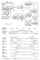
- Fig. 1 is a simplified block-schematic diagram of a optical record player incorporating the teachings of the present invention.
- Fig. 2 shows a set of idealized signal readback waveforms and timing pulses used to describe how the Fig. 1 illustrated recorder/player embodies the present invention.
- Fig. 3 shows simplified idealized signal waveforms for illustrating timing considerations in practicing the present invention.
- Fig. 4. is a schematic of gate logic 30 used in connection with the Figure 3 illustrated waveforms.
- a magnetooptic rotatable disk 10 is suitably supported for rotation by a motor 11 on a frame (not shown).
- a pick-up mechanism 12 is in optical cooperative relationship with the recording surface of disk 10 for optically sensing signals recorded thereon.
- Pick-up 12 can also include electronic amplifiers for amplifying the sensed signals.
- the Fig. 1 illustrated device can also include apparatus for recording signals on disk 10.
- the recording on disk 10 is preferably of a pulse width modulated (PWM) type in which the duration of a pulse is indicative of the information carried by the recorded signal.
- PWM pulse width modulated
- pulse position modulation carries information by a presence or absence of a pulse at a given position on the disk 10 or occurring at a given detection time, also referred to as transition position, which represents one bit of information.
- a PWM pulse can represent any one of a plurality of informational values, i.e., the number 0-4 or 2-7 depending upon the design of the system.
- the present invention is most advantageously employed with PWM recording in that the marks or recorded pulses are some integral number of clock cycles in duration. According to the invention, when the recorded marks or pulses are consistently read as having too long a duration, an amplitude detection threshold is shifted to an increased or higher amplitude value which reduces the effective duration of the pulses for purposes of detection.
- the amplitude threshold is reduced for effectively elongating the mark or pulse readback signals such that an integral number of clock cycles occur for the detection process.
- a phase error in a phase lock loop is measured and used for adjusting the amplitude threshold.
- Such a PWM readback signal is supplied by pick-up 12 over electrical line 14 to threshold derivation circuit 15 as well as to one input of the switching comparator 17.
- Switching comparator 17 receives the threshold derived from the readback signal by circuit 15 through offset summing circuit 16, as later described.
- Switching comparator 17 supplies an output pulse transition over line 34 to pulser 18.
- Pulser 18 shapes the supplied transition of the signal from switching comparator 17 to a pulse which is used for operating the illustrated detection system.
- Data decoder 13 receives the synchronized data from phase lock loop (PLL) or data synchronizer 20.
- Data synchronizer 20 consists of a phase lock loop and a data synchronization circuit. Various forms of data synchronizers may be employed.
- variable frequency oscillator (VFO) 22 is slaved to the operation of the readback signal on line 14.
- Pulser 18 supplies its output pulse to phase detector 24 which compares the timing signals of VFO 22 with the received pulses. Depending upon the detected phase error, detector 24 supplies a negative or a positive signal respectively over lines 32 and 33 to PLL charge pump 25.
- PLL charge pump 25 is constructed in a usual manner for supplying a frequency changing signal through filter 26 to VFO 22.
- Switch 23 receives the pulses from pulser 18 for retiming the pulses to synchronize the timing of the data pulses to the VFO 22 which are then supplied to data decoder 13 in timed relationship to the clock or VFO 22.
- Data decoder 13 is also connected to VFO 22 for synchronizing its operations to the synchronized data from switch 23.
- the adjustment of the derived threshold by circuit 15 is achieved in summing circuit 16.
- the phase errors of VFO 22 operation with respect to the received data pulses from pulser 18 are supplied by phase detector 24 to gate logic 30 respectively over lines 32 and 33.
- the transitions detected by comparator 17 are also supplied over line 34 to gate logic 30.
- Gate logic 30 is constructed as described below in Boolean equations. Such gating logic design depends in part on the design of phase detector 24 and the relative timing involved in the operation of the device. Such design is readily achieved by following the Boolean expressions.
- the term CU and CD represent signals occurring after the detected edge has occurred and respectively indicate a threshold crossing by the readback signal in the upper direction, i.e. the leading edge, or in the downward direction, i.e.
- D means the value of the data from comparator 17; D' indicates a binary zero while a D indicates a binary one.
- DCU means the signal on line 36 while DCD means the signal on line 37.
- Charge pump 38 responds to the up and down indication signals on line 36 and 37 and is constructed like a PLL charge pump 25.
- Filter 39 is comparable to filter 26.
- Charge pump 38 supplies a offset signal through filter 39 to sum circuit 16 which adds or subtracts to the derived threshold value supplied by circuit 15 thereby adjusting the amplitude detection threshold supplied to switching comparator 17.
- a squelch circuit 40 is inserted for selectively squelching the offset and may be desired in some operations. Derivation of detection thresholds from input signals is well known and not further described here except that integration or signal averaging envelope detection may be used as well as other detection systems, such as mean or average amplitudes between peak values.
- the derived threshold may also be held constant after the feedback loop, which adjusts the amplitude threshold, is turned on (via deactivation of the squelch circuit 40).
- Numeral 50 denotes centers of clock periods in the PWM environment.
- Line 14 readback signal 51 is shown as having the value A at a relatively positive excursion and a value A' when relatively negative.
- a desired detection threshold 52 is shown with the location of the detection threshold 52 with respect to the readback waveform 51 is such that the readback waveform 51 amplitude equals detection threshold 52 near the clock centers.
- Numeral 53 denotes an amplitude detection threshold supplied to switching comparator 17 that has too high a threshold for the readback signal 51 and therefore detects a pulse duration of signal 51 that is too short; see pulses 65 and 66 which occur on lines 32 and 33 respectively which produce pulses 72 & 73 respectively on line 37.
- numeral 54 denotes a amplitude detection threshold supplied to switching comparator 17 which has too low in amplitude value resulting in detection of the pulses 61 and 63 which produce pulses 70 & 71 respectively on line 36.
- pulses 61, 63, 65 and 66 on signals 60 and 62 respectively represent jitter in the readback system. Such jitter can cause erroneous data synchronization by data synchronizer 20 resulting in erroneous data being sent to data decoder 13.
- pulses 70 and 71 on DCU line 36 (for the threshold 54 case) and pulses 72 and 73 on DCU line 37 (for the threshold 53 case) are supplied to charge pump 38 for changing its output signal in a known manner through filter 39 for changing the amplitude threshold supplied by offset summer 16 toward the desired amplitude detection threshold 52. Note that the intersection of desired amplitude threshold 52 with the readback signal 51, both on the leading and trailing edges, occurs at a respective one of the clock centers 50.
- Desired data output signal 74 is derived from detection threshold 52. When the detection threshold is at too high a threshold, such as threshold 53, output data signal 75 is produced. Similarly, too low detection threshold 54 produces data output signal 76. Detection using the present invention reliably produces data output signal 74.
- the offset value is a signal indicating media or disk 10 nonuniformities and sensitivity shift with time. Such values can be digitized for processing. It is preferred that such offset values be taken from line 41.
- a detection threshold can be derived from the phase detector feedback without the use of any conventional or prior art threshold variations as provided through offset summer 16.
- Another alternative is to use a phase detector (not shown) separate from the PLL (though using the VFO clock line).
- any type of charge up or charge down integrator may be used instead of a charge pump, followed by a loop filter as is presently practiced and shown in the present application. It is to be remembered that the phase error feedback for adjusting the amplitude detection threshold or for generating an amplitude detection threshold automatically compensates for variations in readback signals derived from magnetooptic media which has been sensitivity shifted with time.
- the signal 51A corresponds generally to signal 51 of Figure 2. Threshold positions 52, 53 and 54 are the same as in Figure 2.
- the desired output data signal 74 corresponds to signal 51A crossing threshold 52 as desired resulting in transitions 87 and 88 in the data pulse aligned with signal 51A crossing the detection threshold at the desired threshold position 52.
- the produced signals from detection are collectively represented by signal 80, i.e. the signals on lines 32, 33, 36 and 37 (Fig. 1) are in substantial time coincidence a short predetermined time after transition 87. If the baseline has shifted downwardly, the threshold position 54 represents the effect of the detection threshold.
- signal 51A exceeds the downwardly baseline shifted detection threshold (detects transition 87 too early) as at vertical line 85 and the downward crossing is detected too late, as represented by vertical dashed line 90.
- the resultant data signal (not shown) corresponds to the positions of the two pulses of signal 82.
- the signals on lines 32, 33, 36 and 37 are substantially time coincident as represented by signal 82 producing a data D signal which is too long.
- the invention causes the detection threshold to be raised until the detection threshold is in the correct relationship with the incoming data.
- threshold position 53 occurs resulting in a too-short data pulse as represented by the signal 81 having pulses time displaced from vertical lines 89 and 86 causing the data signal to be too short as represented by the spacing between the two pulses in signal 81.
- the present invention causes the threshold to be lowered until the detection threshold is in the correct relationship with the incoming data.
Landscapes
- Engineering & Computer Science (AREA)
- Signal Processing (AREA)
- Signal Processing For Digital Recording And Reproducing (AREA)
- Optical Recording Or Reproduction (AREA)
Applications Claiming Priority (2)
| Application Number | Priority Date | Filing Date | Title |
|---|---|---|---|
| US716477 | 1991-06-17 | ||
| US07/716,477 US5204848A (en) | 1991-06-17 | 1991-06-17 | Adjusting amplitude detection threshold by feeding back timing-data phase errors |
Publications (3)
| Publication Number | Publication Date |
|---|---|
| EP0519684A2 EP0519684A2 (en) | 1992-12-23 |
| EP0519684A3 EP0519684A3 (en) | 1993-03-03 |
| EP0519684B1 true EP0519684B1 (en) | 1998-04-01 |
Family
ID=24878139
Family Applications (1)
| Application Number | Title | Priority Date | Filing Date |
|---|---|---|---|
| EP92305512A Expired - Lifetime EP0519684B1 (en) | 1991-06-17 | 1992-06-16 | Reading signals for optical storage media |
Country Status (8)
| Country | Link |
|---|---|
| US (1) | US5204848A (ja) |
| EP (1) | EP0519684B1 (ja) |
| JP (1) | JP2804997B2 (ja) |
| KR (1) | KR960004579B1 (ja) |
| AR (1) | AR245308A1 (ja) |
| BR (1) | BR9202157A (ja) |
| CA (1) | CA2064633C (ja) |
| DE (1) | DE69224936T2 (ja) |
Families Citing this family (17)
| Publication number | Priority date | Publication date | Assignee | Title |
|---|---|---|---|---|
| JP2807362B2 (ja) * | 1991-09-30 | 1998-10-08 | 株式会社東芝 | 情報再生装置 |
| JP3184688B2 (ja) * | 1993-12-10 | 2001-07-09 | キヤノン株式会社 | 光学的情報再生装置 |
| US5790495A (en) | 1994-05-06 | 1998-08-04 | Discovision Associates | Data generator assembly for retrieving stored data by comparing threshold signal with preprocessed signal having DC component |
| US5894468A (en) * | 1994-05-06 | 1999-04-13 | Discovision Associates | Data recovery with differentiation and partial integration stages to eliminate noises and DC offset level |
| AU741101B2 (en) * | 1994-05-06 | 2001-11-22 | Discovision Associates | A method for retrieving data stored on a medium |
| US5396479A (en) * | 1994-05-06 | 1995-03-07 | Maxoptix Corporation | Apparatus and method for setting a threshold level to maintain duty cycle in a pulse width modulated optical recording system |
| US5739969A (en) * | 1994-07-26 | 1998-04-14 | Inwave Technologies, Inc. | Digital data storage using predetermined increments of time wherein each increment represents a plurality of bits of information |
| US5777967A (en) * | 1995-04-05 | 1998-07-07 | Matsushita Electric Industrial Co., Ltd. | Optical disk device |
| US5612938A (en) * | 1995-04-20 | 1997-03-18 | Eastman Kodak Company | Correcting recorded marks and land lengths taken from an optical disk |
| US5757751A (en) * | 1996-01-16 | 1998-05-26 | International Business Machines Corporation | Baseline correction circuit for pulse width modulated data readback systems |
| DE19715274A1 (de) | 1997-04-12 | 1998-10-15 | Thomson Brandt Gmbh | Gerät zum Lesen und/oder Beschreiben optischer Aufzeichnungsträger |
| JP3758306B2 (ja) * | 1997-06-12 | 2006-03-22 | パイオニア株式会社 | 記録媒体の傷検出装置及びこれを用いた読取装置 |
| US6631103B1 (en) * | 1998-04-09 | 2003-10-07 | Texas Instruments Incorporated | Jitter feedback slicer |
| JP3017167B2 (ja) * | 1998-05-20 | 2000-03-06 | インターナショナル・ビジネス・マシーンズ・コーポレイション | デ一タ記憶媒体からのリ一ド信号の2値化方法および装置 |
| FR2779263B1 (fr) * | 1998-06-02 | 2000-08-25 | Atg Sa | Procede et dispositif de correction automatique du seuil de detection des donnees enregistrees sur un disque optique numerique |
| US7423948B2 (en) * | 2003-09-09 | 2008-09-09 | Matsushita Electric Industrial Co., Ltd. | Phase error detecting circuit and synchronization clock extraction circuit |
| WO2021051454A1 (zh) | 2019-09-30 | 2021-03-25 | 深圳市速腾聚创科技有限公司 | 激光雷达振镜的控制方法、控制装置和激光雷达 |
Family Cites Families (27)
| Publication number | Priority date | Publication date | Assignee | Title |
|---|---|---|---|---|
| US3483539A (en) * | 1966-03-11 | 1969-12-09 | Potter Instrument Co Inc | Pulse repositioning system |
| US3893171A (en) * | 1974-03-25 | 1975-07-01 | Ibm | Signal adjustment circuit |
| DE2513852C3 (de) * | 1974-04-04 | 1988-07-28 | Sharp K.K., Osaka | Anordnung zum automatischen Aufsuchen der nächsten Magnetbandaufzeichnungslücke |
| JPS5147324A (en) * | 1974-10-21 | 1976-04-22 | Sony Corp | Karaaeizoshingono saiseisochi |
| JPS5247319A (en) * | 1975-10-13 | 1977-04-15 | Victor Co Of Japan Ltd | Recording/reproducing system of color video signal |
| FR2358797A1 (fr) * | 1976-07-16 | 1978-02-10 | Thomson Brandt | Systeme de correction automatique du facteur de forme de l'onde porteuse issue de la lecture d'un support d'information |
| US4426667A (en) * | 1978-05-17 | 1984-01-17 | Savin Corporation | Pulse width modulation system |
| US4356506A (en) * | 1979-06-18 | 1982-10-26 | Matsushita Electric Industrial Co. Ltd. | Automatic chrominance control circuit for a color video tape recorder |
| JPS5671856A (en) * | 1979-11-15 | 1981-06-15 | Sony Corp | Playback device of disc |
| NL8000121A (nl) * | 1980-01-09 | 1981-08-03 | Philips Nv | Schijfvormige, optische uitleesbare registratiedrager als opslagmedium voor datainformatie, inrichting voor het vervaardigen van zo'n registratiedrager, inrichting voor het optekenen van datainformatie in zo'n registratiedrager en inrichting voor het uitlezen van zo'n registratiedrager. |
| NL191374C (nl) * | 1980-04-23 | 1995-06-16 | Philips Nv | Communicatiesysteem met een communicatiebus. |
| JPS56160189A (en) * | 1980-04-29 | 1981-12-09 | Sony Corp | Differential gain compensating circuit |
| JPS5757025A (en) * | 1980-09-24 | 1982-04-06 | Sony Corp | Waveform converting circuit |
| JPS5977633A (ja) * | 1982-10-26 | 1984-05-04 | Nippon Gakki Seizo Kk | デイスク再生装置におけるクロツク再生回路 |
| JPS5977605A (ja) * | 1982-10-26 | 1984-05-04 | Sansui Electric Co | 読取りクロツク生成方式 |
| JPS59152512A (ja) * | 1983-02-21 | 1984-08-31 | Toshiba Corp | デジタルデ−タ生成装置 |
| FR2548814B1 (fr) * | 1983-07-04 | 1986-05-02 | Thomson Csf | Procede et dispositif de remise en forme d'un signal de lecture de donnees enregistrees sur disque optique |
| US4580176A (en) * | 1983-11-21 | 1986-04-01 | International Business Machines Corporation | Adaptive equalization circuit for magnetic recording channels utilizing signal timing |
| JPS6267731A (ja) * | 1985-09-20 | 1987-03-27 | Fujitsu Ltd | 光記録再生方法及び光記録再生装置 |
| DE3781698T2 (de) * | 1986-02-07 | 1993-02-11 | Matsushita Electric Ind Co Ltd | Geraet zur wiedergabe von digitalinformationen. |
| JPH0727606B2 (ja) * | 1986-12-11 | 1995-03-29 | ソニー株式会社 | 記録型光デイスクに対する磁界印加装置 |
| JPH0719445B2 (ja) * | 1987-12-17 | 1995-03-06 | パイオニア株式会社 | 記録再生用クロック生成回路 |
| JPS63285774A (ja) * | 1987-05-19 | 1988-11-22 | Hitachi Ltd | 信号2値化回路 |
| JPH01130324A (ja) * | 1987-11-16 | 1989-05-23 | Olympus Optical Co Ltd | 光学的記録再生装置 |
| JP2568110B2 (ja) * | 1988-07-15 | 1996-12-25 | パイオニア株式会社 | フェーズロックドループ回路 |
| US5062005A (en) * | 1989-02-01 | 1991-10-29 | Matsushita Electric Industrial Co., Ltd. | Videodisc reproducing apparatus |
| JPH03171453A (ja) * | 1989-11-29 | 1991-07-24 | Sony Corp | 光磁気信号再生方法 |
-
1991
- 1991-06-17 US US07/716,477 patent/US5204848A/en not_active Expired - Fee Related
-
1992
- 1992-04-01 CA CA002064633A patent/CA2064633C/en not_active Expired - Fee Related
- 1992-05-13 JP JP4120574A patent/JP2804997B2/ja not_active Expired - Fee Related
- 1992-05-15 KR KR1019920008230A patent/KR960004579B1/ko not_active Expired - Fee Related
- 1992-06-05 BR BR929202157A patent/BR9202157A/pt not_active Application Discontinuation
- 1992-06-12 AR AR92322543A patent/AR245308A1/es active
- 1992-06-16 EP EP92305512A patent/EP0519684B1/en not_active Expired - Lifetime
- 1992-06-16 DE DE69224936T patent/DE69224936T2/de not_active Expired - Fee Related
Also Published As
| Publication number | Publication date |
|---|---|
| US5204848A (en) | 1993-04-20 |
| EP0519684A2 (en) | 1992-12-23 |
| CA2064633A1 (en) | 1992-12-18 |
| JPH05144192A (ja) | 1993-06-11 |
| EP0519684A3 (en) | 1993-03-03 |
| DE69224936D1 (de) | 1998-05-07 |
| KR960004579B1 (ko) | 1996-04-09 |
| CA2064633C (en) | 1997-05-13 |
| KR930001185A (ko) | 1993-01-16 |
| JP2804997B2 (ja) | 1998-09-30 |
| BR9202157A (pt) | 1993-02-02 |
| AR245308A1 (es) | 1993-12-30 |
| DE69224936T2 (de) | 1998-10-22 |
Similar Documents
| Publication | Publication Date | Title |
|---|---|---|
| EP0519684B1 (en) | Reading signals for optical storage media | |
| US5677802A (en) | Phase locked loop circuit with adjustable offset characteristic, method for adjustment and apparatus | |
| US5585975A (en) | Equalization for sample value estimation and sequence detection in a sampled amplitude read channel | |
| CA2148748C (en) | Method and apparatus for retreiving data from a storage device | |
| JP3345515B2 (ja) | ピークシフト補正回路およびそれを使用した磁気記録媒体再生装置 | |
| US6320834B1 (en) | Data demodulating method and optical disk device using the method | |
| US6078451A (en) | Method and apparatus for adjusting data window phase when retrieving data stored on a recording medium | |
| US5568465A (en) | Reading from record medium in either an inverted or non-inverted signal-processing mode | |
| JP3347468B2 (ja) | 情報再生装置 | |
| US5986990A (en) | Device for detecting digital bit in optical disc reproducing apparatus | |
| US5396479A (en) | Apparatus and method for setting a threshold level to maintain duty cycle in a pulse width modulated optical recording system | |
| US5523896A (en) | Variable speed reproducing apparatus for a digital video cassette recorder | |
| JPH08315518A (ja) | デジタル信号用信号処理装置 | |
| US6374035B1 (en) | Signal processing device | |
| MY118089A (en) | Optical disc reproduction apparatus capable of correcting a characteristic of an equalizer | |
| US5467232A (en) | Magnetic recording and reproducing method using phase discrimination and apparatus therefor | |
| GB2325079A (en) | Automatic bandwidth control in a waveform equalizer | |
| JP3684589B2 (ja) | ディジタル信号再生装置 | |
| JP3505923B2 (ja) | 情報処理装置および情報記録装置 | |
| CA2259838C (en) | Method and apparatus for retrieving data from a storage device | |
| JP2001067816A (ja) | ディスク再生装置 | |
| JP3488074B2 (ja) | ディジタル記録再生装置 | |
| JPH07334930A (ja) | 再生装置 | |
| JPH0581691A (ja) | デイスク装置 | |
| JPH04341928A (ja) | 光ディスク再生信号パルス自動補正装置 |
Legal Events
| Date | Code | Title | Description |
|---|---|---|---|
| PUAI | Public reference made under article 153(3) epc to a published international application that has entered the european phase |
Free format text: ORIGINAL CODE: 0009012 |
|
| AK | Designated contracting states |
Kind code of ref document: A2 Designated state(s): DE FR GB IT |
|
| PUAL | Search report despatched |
Free format text: ORIGINAL CODE: 0009013 |
|
| AK | Designated contracting states |
Kind code of ref document: A3 Designated state(s): DE FR GB IT |
|
| 17P | Request for examination filed |
Effective date: 19930427 |
|
| 17Q | First examination report despatched |
Effective date: 19951018 |
|
| GRAG | Despatch of communication of intention to grant |
Free format text: ORIGINAL CODE: EPIDOS AGRA |
|
| GRAG | Despatch of communication of intention to grant |
Free format text: ORIGINAL CODE: EPIDOS AGRA |
|
| GRAG | Despatch of communication of intention to grant |
Free format text: ORIGINAL CODE: EPIDOS AGRA |
|
| GRAH | Despatch of communication of intention to grant a patent |
Free format text: ORIGINAL CODE: EPIDOS IGRA |
|
| GRAH | Despatch of communication of intention to grant a patent |
Free format text: ORIGINAL CODE: EPIDOS IGRA |
|
| GRAA | (expected) grant |
Free format text: ORIGINAL CODE: 0009210 |
|
| AK | Designated contracting states |
Kind code of ref document: B1 Designated state(s): DE FR GB IT |
|
| ITF | It: translation for a ep patent filed | ||
| REF | Corresponds to: |
Ref document number: 69224936 Country of ref document: DE Date of ref document: 19980507 |
|
| ET | Fr: translation filed | ||
| PLBE | No opposition filed within time limit |
Free format text: ORIGINAL CODE: 0009261 |
|
| STAA | Information on the status of an ep patent application or granted ep patent |
Free format text: STATUS: NO OPPOSITION FILED WITHIN TIME LIMIT |
|
| 26N | No opposition filed | ||
| PGFP | Annual fee paid to national office [announced via postgrant information from national office to epo] |
Ref country code: FR Payment date: 19990614 Year of fee payment: 8 |
|
| PG25 | Lapsed in a contracting state [announced via postgrant information from national office to epo] |
Ref country code: FR Free format text: LAPSE BECAUSE OF NON-PAYMENT OF DUE FEES Effective date: 20010228 |
|
| REG | Reference to a national code |
Ref country code: FR Ref legal event code: ST |
|
| REG | Reference to a national code |
Ref country code: GB Ref legal event code: IF02 |
|
| PGFP | Annual fee paid to national office [announced via postgrant information from national office to epo] |
Ref country code: GB Payment date: 20030602 Year of fee payment: 12 |
|
| PGFP | Annual fee paid to national office [announced via postgrant information from national office to epo] |
Ref country code: DE Payment date: 20030624 Year of fee payment: 12 |
|
| PG25 | Lapsed in a contracting state [announced via postgrant information from national office to epo] |
Ref country code: GB Free format text: LAPSE BECAUSE OF NON-PAYMENT OF DUE FEES Effective date: 20040616 |
|
| PG25 | Lapsed in a contracting state [announced via postgrant information from national office to epo] |
Ref country code: DE Free format text: LAPSE BECAUSE OF NON-PAYMENT OF DUE FEES Effective date: 20050101 |
|
| GBPC | Gb: european patent ceased through non-payment of renewal fee |
Effective date: 20040616 |
|
| PG25 | Lapsed in a contracting state [announced via postgrant information from national office to epo] |
Ref country code: IT Free format text: LAPSE BECAUSE OF NON-PAYMENT OF DUE FEES Effective date: 20050616 |