EP0507601B1 - Procédé et appareil de traitement d'images - Google Patents
Procédé et appareil de traitement d'images Download PDFInfo
- Publication number
- EP0507601B1 EP0507601B1 EP92302946A EP92302946A EP0507601B1 EP 0507601 B1 EP0507601 B1 EP 0507601B1 EP 92302946 A EP92302946 A EP 92302946A EP 92302946 A EP92302946 A EP 92302946A EP 0507601 B1 EP0507601 B1 EP 0507601B1
- Authority
- EP
- European Patent Office
- Prior art keywords
- colour
- image
- monochrome
- encoding
- data
- Prior art date
- Legal status (The legal status is an assumption and is not a legal conclusion. Google has not performed a legal analysis and makes no representation as to the accuracy of the status listed.)
- Expired - Lifetime
Links
Images


Classifications
-
- H—ELECTRICITY
- H04—ELECTRIC COMMUNICATION TECHNIQUE
- H04N—PICTORIAL COMMUNICATION, e.g. TELEVISION
- H04N1/00—Scanning, transmission or reproduction of documents or the like, e.g. facsimile transmission; Details thereof
- H04N1/41—Bandwidth or redundancy reduction
-
- H—ELECTRICITY
- H04—ELECTRIC COMMUNICATION TECHNIQUE
- H04N—PICTORIAL COMMUNICATION, e.g. TELEVISION
- H04N1/00—Scanning, transmission or reproduction of documents or the like, e.g. facsimile transmission; Details thereof
- H04N1/46—Colour picture communication systems
- H04N1/64—Systems for the transmission or the storage of the colour picture signal; Details therefor, e.g. coding or decoding means therefor
- H04N1/642—Adapting to different types of images, e.g. characters, graphs, black and white image portions
-
- G—PHYSICS
- G09—EDUCATION; CRYPTOGRAPHY; DISPLAY; ADVERTISING; SEALS
- G09G—ARRANGEMENTS OR CIRCUITS FOR CONTROL OF INDICATING DEVICES USING STATIC MEANS TO PRESENT VARIABLE INFORMATION
- G09G2310/00—Command of the display device
- G09G2310/02—Addressing, scanning or driving the display screen or processing steps related thereto
- G09G2310/0202—Addressing of scan or signal lines
- G09G2310/0205—Simultaneous scanning of several lines in flat panels
- G09G2310/0208—Simultaneous scanning of several lines in flat panels using active addressing
-
- G—PHYSICS
- G09—EDUCATION; CRYPTOGRAPHY; DISPLAY; ADVERTISING; SEALS
- G09G—ARRANGEMENTS OR CIRCUITS FOR CONTROL OF INDICATING DEVICES USING STATIC MEANS TO PRESENT VARIABLE INFORMATION
- G09G3/00—Control arrangements or circuits, of interest only in connection with visual indicators other than cathode-ray tubes
- G09G3/20—Control arrangements or circuits, of interest only in connection with visual indicators other than cathode-ray tubes for presentation of an assembly of a number of characters, e.g. a page, by composing the assembly by combination of individual elements arranged in a matrix no fixed position being assigned to or needed to be assigned to the individual characters or partial characters
- G09G3/2007—Display of intermediate tones
- G09G3/2014—Display of intermediate tones by modulation of the duration of a single pulse during which the logic level remains constant
-
- G—PHYSICS
- G09—EDUCATION; CRYPTOGRAPHY; DISPLAY; ADVERTISING; SEALS
- G09G—ARRANGEMENTS OR CIRCUITS FOR CONTROL OF INDICATING DEVICES USING STATIC MEANS TO PRESENT VARIABLE INFORMATION
- G09G3/00—Control arrangements or circuits, of interest only in connection with visual indicators other than cathode-ray tubes
- G09G3/20—Control arrangements or circuits, of interest only in connection with visual indicators other than cathode-ray tubes for presentation of an assembly of a number of characters, e.g. a page, by composing the assembly by combination of individual elements arranged in a matrix no fixed position being assigned to or needed to be assigned to the individual characters or partial characters
- G09G3/2007—Display of intermediate tones
- G09G3/2018—Display of intermediate tones by time modulation using two or more time intervals
Definitions
- the invention relates to an image processing method and apparatus in, for instance, an image communicating apparatus, an image storing apparatus, or the like. It has been known to process colour image data by a binary data process in which colour data for each of the colours red, green, blue, cyan, magenta, yellow, white and black are handled as binary data.
- JP-A-63190474 discloses an image processing apparatus having, as in the preamble of claim 1 attached:
- two channels are provided, one for binary data processing and the other for multi-level data processing.
- the data stored in one or other channel is selected depending on the type of image represented by the input image data - e.g. either a character image or a pictorial image.
- the invention is made in consideration of the circumstances as mentioned above and it is an object of the invention to provide an image processing method and an apparatus which can efficiently transmit image data.
- an image processing apparatus characterised by: extracting means for extracting monochrome image data from the colour image data input by said input means; monochrome image encoder means for encoding the monochrome image data and for generating monochrome code data, the encoding of said monochrome image encoder means being different from that of said colour image encoder means; storage means for storing said colour code data and said monochrome code data, said colour image data and said monochrome image data representing the same original image; and output means for selectively outputting said colour code data or said monochrome code data stored by said storage means.
- JP-A-61065663 the case is considered where the receiver is a printer loaded with colour film paper.
- image data transmitted is monochrome and not colour image data, it is detected that such data is unsuitable for colour printing, and transmission is interrupted. Transmission is also interrupted in a case where colour image data is transmitted from a transmitter and the receiver is loaded with monochrome film paper. In either case, wasteful consumption of film paper is avoided. However, no useful transmission can be performed in such cases.
- the embodiment has first encoding means and second encoding means for encoding a colour image, wherein the colour image to be encoded is simultaneously encoded by both of the systems, thereby obtaining the encoded data. After that, the encoding system which is optimum for the encoded colour image is selected and the colour image is transmitted. After the colour image has been encoded by both of the systems, the encoding ability on the reception side is confirmed by a protocol and the proper encoded data is subsequently transmitted, so that the image can be promptly transmitted. Before the encoded data is transmitted, the user can also check the code length and select the code data to be transmitted. By decoding both of the codes on the transmission side, the degree of deterioration of the colour image can be also checked.
- Reference numeral 20 denotes a colour image input unit. For instance, a colour image is scanned by a colour scanner and multilevel colour image signals each comprising eight bits of red (R), green (G), and blue (B) indicative of a full colour image are supplied to signal lines 101, 102, and 103, respectively.
- Reference numerals 21, 22 and 23 denote a section to form a binary colour encoder channel.
- Reference numeral 21 denotes a binarisation unit to convert data or R, G, and B each consisting of eight bits into RGB data each consisting of one bit for each colour.
- Reference numeral 22 denotes a binary colour image encode unit to encode the binarised RGB data.
- the RGB signals 101, 102 and 103 supplied from the colour image input unit 20 are converted into RGB signals each consisting of one bit by the binarisation unit and, thereafter, they are compressed and encoded by the binary colour image encode unit, thereby forming a binary code bit stream 110.
- the code data is stored in a binary image encoded data storage unit 23 and is held until the image signal is transmitted.
- An auxiliary storage device such as a hard disk, is used as the storage unit 23.
- the 8-bit output signals of R, G, and B colours from the colour image input unit 20 are also supplied to a multilevel colour image encode unit 24 and encoded.
- the encode unit 24 they are compressed and encoded by a DCT conversion encoding in a state of the multilevel data and stored in a multilevel image encoded data storage unit 25.
- both of the binary image code data and the multilevel image code data are simultaneously formed from the same colour image by the two kinds of encoder units 22 and 24. When the image is transmitted, either one of the two kinds of code data is selected.
- colour images are reconstructed by a binary colour image decoder unit 28 and a multilevel colour image decode unit 29, respectively.
- a binary colour image decoder unit 28 By displaying the decoded images on a display 31 by a control unit 30, the picture quality of the image, which is to be transmitted, can be known.
- a communications control unit 27 executes a communication protocol to a transmission partner, thereby checking the decoding ability of the reception side.
- the reception side has an ability enough to decode any of the binary image code data and the multilevel image code data, the operator can select and transmit either one of the images by an operation unit 32.
- the reception side When the reception side has a decoding ability of only either one of them, the image to be transmitted is indicated to the operator and, after that, it is sent from a communication processing unit 31 to a digital line (not shown) such as an ISDN or the like.
- a communication processing unit 31 such as an ISDN or the like.
- the protocol is based on the well-known G4 protocol.
- any one of the simple binarisation, dither process, and error diffusion process can be selected. Since those binarising processes are well known, their descriptions are omitted here.
- Fig. 2 is a block diagram of the binary colour image encode unit 22.
- An R signal 104, a G signal 105, and a B signal 106 as binarised outputs from the binarisation unit 21 (Fig.1) are supplied to a prediction state determination circuit 50.
- the prediction state determination circuit 50 generates a prediction state signal S116 comprising peripheral encoded pixels around a target pixel and also generates a 1-bit pixel signal X117 synchronised with the prediction state signal S116. Those two signals S116 and X117 are encoded in a dynamic arithmetic encode unit 51, so that the binary image code data 110 is generated.
- Fig. 3 is a block diagram of the prediction state determination circuit 50.
- Figs. 4A to 4C show pixel positions of respective colours which are referred for state prediction.
- FIG. 4A shows the reference pixels of the first colour (R in the embodiment) to be encoded. Seven peripheral encoded pixels around the encode pixel indicated by "*" are referred to.
- Fig. 4B shows the reference pixels of the second colour (G in the embodiment) for encoding. Eight pixels comprising the seven pixels similar to those shown in Fig. 4A and the pixel at the same position as that of the first colour are referred to.
- Fig. 4C shows the reference pixels of the third colour (B in the embodiment).
- Nine pixels comprising the seven pixels similar to those shown in Fig. 4A and the pixels at the same positions as those of the first and second colours are referred to.
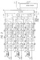
- the binarised image signals 104, 105 and 106 of R, G and B each consisting of one bit are supplied to latches 67 to 69 and to line memories 61 to 63.
- the R, G and B data delayed by one line are held by the line memories 61 to 63.
- the data delayed every one pixel clock are held in latches 67a to 67h, 68a to 68h, and 69a to 69h, respectively.
- the data of the pixels on the preceding line of the encode line can be referred by the outputs in the latches 67a to 67d into which the outputs of the line memory 61 are supplied and by the output of the line memory 61.
- the two encoded pixels on the encode line can be referred by the outputs in the latches 67g and 67h.
- the data of those seven pixels assumes a reference pixel signal 210 for determination of the state of R as a first colour for encoding.
- Data 211 of R of the encode pixel is generated from the latch 67f in order to determine states of the other colours G and B.
- the latch groups 68 and 69 having substantially the same construction as the latch group 67 are provided for data G105 and B106. Data of seven pixels similar to that of the latch group 67 are generated as reference pixel signals 212 and 214 from the latch groups 68 and 69, respectively.
- Data 213 of G of the encode pixels is generated from the latch 68f in the latch group 68 in order to determine a state of B.
- a selector 64 switches the reference pixel signals in accordance with a colour indication signal 219 of two bits indicative of the color corresponding to the output of each colour data of R, G, and B. That is, when the colour indication signal 219 indicates R, the reference pixel signal 210 and a zero signal of two bits are selected. When the signal 219 indicates G, the reference pixel signal 212, R signal 211, and zero signal of one bit are selected. In the case of B, the reference pixel signal 214, R signal 211, and G signal 213 are selected.
- a selection signal 215 of nine bits and the colour indication signal 219 of two bits are combined to a signal of eleven bits by a packing circuit 65 and becomes the prediction state signal S116. Therefore, a state signal S 1 indicates the colour of the pixel to be encoded and the peripheral state and shows 2 7 states, 2 8 states, and 2 9 states for the colours R, G, and B, respectively.
- the pixel signals which are synchronized with the prediction states of the respective colours R, G, and B and which should be encoded are generated from R211, B213, and G216 and are selected by the selector 64 in accordance with the colour indication signal 219, so that the pixel signal X117 is generated.
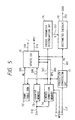
- Fig. 5 is a block diagram of the dynamic arithmetic encoder unit 51 shown in Fig. 2.
- an arithmetic code is based on a method whereby a code is formed by an arithmetic operation in a manner such that an input signal train becomes a code which is expressed by decimal binary number.
- a method is proposed in the literature by Langdon, Rissanen, et. al., "Compression of Black/White Images with Arithmetic Coding", IEEE Transaction Com. COM-29, 6, June, 1981, or the like.
- the encoded data indicates a more priority symbol (MPS: 0 in the above example)
- A(S 0 ) and C(S 0 ) are used to encode the next data.
- the less priority symbol LPS: 1 in the above example
- A(S 1 ) and C(S 1 ) are used to encode the next data.
- the value of new A is increased by 2 S times (S is an integer of 0 or more) and is set to a value within a range of 0.5 ⁇ A ⁇ 1.0.
- S is an integer of 0 or more
- the above process corresponds to that the arithmetic register A is shifted S times in the hardware.
- the code register C is also shifted by the same number of times and the shifted-out signal becomes the code.
- the code is formed by repeating the above processes.
- the embodiment uses a dynamic method whereby a probability is presumed while encoding as mentioned above.
- the state signal S116 from the packing circuit 65 shown in Fig. 3 is supplied to a counter memory 73 and an encode condition memory 74.
- a more priority symbol MPS 308 as a symbol which can easily appear and an index I307 indicative of the encode condition including an appearance probability of the LPS of the arithmetic code, which will be explained hereinlater, are stored in the encode condition memory 74 every state which is expressed by the state signal S116.
- the MPS 308 read out from the memory 74 in accordance with the color and state of the image to be encoded is supplied to a prediction conversion circuit 77.
- the prediction conversion circuit 77 forms a YN signal 301 which is set to 0 when the serial pixel signal X117 from the selector 64 shown in Fig. 3 coincides with the MPS 308.
- the YN signal 301 is supplied to an update circuit 75.
- the update circuit 75 increases a count value in a corresponding state among the count values stored in the counter memory 73 when the YN signal is equal to 0.
- a count value C306 stored in the counter memory 73 coincides with a set value MC305 from a count table ROM 72
- the count value is updated in such a direction as to increase the index I307 (direction as to decrease the appearance probability q of the LPS) (in this case, the MPS is not inverted).
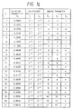
- the count table ROM 72 supplies the number MC305 of MPSs shown in Fig. 11 which has been predetermined in correspondence to an index I representing the appearance probability q of the LPS to he update circuit 75.
- the update circuit 75 updates the count value in such a direction as to reduce the index I307 (direction as to increase the appearance probability q of the LPS) when the MPS 308 and the pixel signal X117 are different, that is, when the YN signal from the prediction conversion circuit 77 is equal to 1.
- the YN signal whose value is equal to 1 is given in the case where the index is equal to 1, a process to invert the MPS (0 ⁇ 1 or 1 ⁇ 0) is executed.
- Outputs I' 309 and MPS' 310 of the update circuit 75 denote the values of the index after updating and are again stored into the encode condition memory 74.
- An encode parameter determination circuit 76 sets an encode parameter Q311 of the arithmetic code into an arithmetic encoder 78 on the basis of the value of the index I307.
- the arithmetic encoder 78 arithmetically encodes the YN signal 301 from the prediction conversion circuit 77 by using the parameter Q311, thereby obtaining a code 302.
- a static encoding can be easily realized by a method whereby an initial value is preliminarily given to the encode condition memory 74 and I and MPS are not updated.
- Fig. 6 is a block diagram of the prediction conversion circuit 77.
- the serial pixel signal X117 and the MPS 308 are supplied to an EX-OR circuit 79.
- the EX-OR circuit 79 generates the YN signal 301 which is set to 0 when the serial pixel signal X117 and the MPS 308 coincide and which is set to 1 when they differ in accordance with logic expressions of Fig. 13.
- Fig. 7 is a block diagram of the update circuit 75.
- the count value C306 from the counter memory 73 is increased by +1 by an adder 81, so that a signal C' 312 is derived.
- the value of the signal C' 312 is compared with the MC305 from the count table ROM 72 by a comparator 83.
- an update signal UPA 313 is set to 1.
- the YN signal 301 becomes an update signal UPB 314.
- the signals UPA and UPB are supplied to an index change circuit 85.
- the OR of UPA and UPB is calculated by an OR circuit 87.
- An output signal 315 of the OR circuit 87 is used as a switching signal of a selector 82.
- the selector 82 selects a 0 signal 319 to reset the value of the counter memory 73 when the signal 315 is equal to 1.
- the selector 82 selects the output signal C' 312 of the adder 81.
- the selector 82 generates the selected signal as a counter update signal C" 316 and stores into the counter memory 73. Therefore, when the serial pixel signal X117 and the MPS 308 are different and when a state in which they coincide continues a predetermined number of times, the count value of the counter memory 73 is reset.
- the updated index I' is determined by referring to the table on the basis of the present index I, update slice condition d, UPA, and UPB.
- an EX signal 318 is set.
- the EX signal 318 is equal to 1
- an inverter 86 inverts the symbol of the present MPS 308 (0 ⁇ 1 or 1 ⁇ 0), thereby obtaining the update MPS' 310.
- the EX signal is equal to 0, the MPS' is not changed.
- the updated I' 309 and the MPS' 310 are stored into the encode condition memory 74 and are used as an index I and an MPS for the next process.
- the updating method shown in Fig. 13 can be also constructed by a table using an ROM or the like or can be also realized by a logic construction using adders and subtracters.
- the MPSs of the number which is equal to a predetermined number of MPSs according to the value of the index I representing the appearance probability q of the LPS which has been approximated by the polynomial of the power of 2 are generated, the value of d is added to the value of index I, thereby reducing the appearance probability q of the LPS which is used in the arithmetic code.
- LPSs when LPSs are generated, d is subtracted from the index 1, thereby increasing the appearance probability q of LPS which is used in the arithmetic code.
- LPSs are generated in a state showing that the appearance probability q of LPS is equal to 0.5 (state in which the index I is equal to 1), the MPS is inverted.
- the arithmetic encoding of a high encoding efficiency can be accomplished.
- Fig. 8 shows encoding efficiency curves of the arithmetic code which is used in the embodiment.
- the value of index I is shown by a small letter i hereinbelow.
- the curves are expressed by the equation (6) when it is assumed that the appearance probability of LPS is set to q and an approximate probability upon encoding is set to q ei .
- the indices I of 1, 2, 3, ... are sequentially given to the values of the appearance probabilities q of LPS in accordance with the order from the larger value to the smaller value.
- ⁇ -qlog 2 q-(1-q)log 2 (1-q) -qlog 2 q ei -(1-q)log 2 (1-q ei )
- the effective probability q ei shown in Fig. 14 is selected from the probabilities which can be approximated by two terms.
- Q 1 , Q 2 , and Q 3 of Fig. 15 are parameters Qc 311 which are sent to the arithmetic encoder 78. That is, Q 1 and Q 2 denote shift amounts which are given to the shift register. The power of 2 is calculated by the shift operations.
- Q 3 indicates a coefficient of the second term and the switching between + and - is executed.
- N M N L (1/q-1)
- the number N Mi of more priority symbols MPS corresponding to each index I is obtained on the basis of each boundary probability q bi as shown in Fig. 8.
- a difference between the numbers N M of more priority symbols of the adjacent indices is set to MC for each index I.
- the value of MC is compared with the number of more priority symbols MPS generated as mentioned above. When they coincide, such a state is determined to be a state in which the encoding using the adjacent index I is suitable, so that the index I is changed. Consequently, the index I is changed at a proper timing on the basis of the number of more priority symbols MPS generated and the encoding using the optimum index I can be adaptively accomplished.
- Fig. 9 is a block diagram of the arithmetic encoder 78.
- Q 1 is supplied to a shift register A 90
- Q 2 is supplied to a shift register B 91
- Q 3 is supplied to a selector 92.
- Q 1 and Q 2 indicate by which number of bits an Augend signal As 323 is shifted to the right for the shift registers A and B. The results of the shift are generated as output signals 330 and 331.
- a complementary number of the signal 331 is obtained by an inverter 96.
- the selector 92 selects either the signal 331 or an output signal of the inverter 96 in accordance with a control signal Q 3 , so that an output signal 332 is derived.
- An adder 93 adds the signal 330 from the shift register A 90 and the signal 332 from the selector 92 and generates an A S1 signal 324.
- a subtracter 94 subtracts the A S1 signal 324 from the As signal 323, thereby obtaining an A S0 signal 325.
- a selector 95 selects either the A S0 signal 325 or the A S1 signal 324 by the YN signal 301. That is, the A S0 signal is selected when the YN signal is equal to 1.
- the A S1 signal is selected when the YN signal is equal to 0. Thus, the selected signal is generated as an A' signal 326.
- a shift circuit 89 executes a process to shift to the left until the MSB of the A' signal is equal to 1.
- An AS' signal 327 is derived by the shifting process.
- the shift signal 332 corresponding to the number of shifting processes is supplied to a code register 99. The bits of the number corresponding to the number of shifting processes are sequentially generated from the code register 99 in accordance with the order from the MSB, so that the code data 330 is derived.
- the code data 330 is processed by a bit processing method (not shown) in a manner such that the number of continuous bits 1 is set to a finite value.
- a content CR 328 of the code register 99 is added to the A S0 signal 325 by an adder 97 and a resultant data is supplied to a selector 98.
- the signal Cr 328 to which the A S0 signal 325 is not added is also supplied to the selector 98.
- a CR' signal 329 is generated.
- the CR' signal 329 is set to CR when the YN signal 301 is equal to 1 and is set to CR + A S0 when the YN signal is equal to 0.
- the foregoing shifting process regarding the code register 99 is also executed for the CR' signal.
- the binary RGB colour encode data (code data 330 shown in Fig. 9) produced as mentioned above is stored into the binary image encoded data storage unit 23 through a data line 110 shown in Fig. 1A.
- Fig. 10 is a block diagram of the conversion unit 10 and the multilevel colour image encoder unit 24 shown in Fig. 1A.
- the gradation data 101, 102 and 103 of RGB each consisting of eight bits which are supplied from the colour image input unit 20 in Fig.
- the YUV signals are subjected to a two-dimensional discrete cosine transformation in a DCT circuit 11 and separated every spatial frequency component.
- the spatial frequency components are called DCT conversion coefficients.
- a converting equation of the discrete cosine transformation is shown below.
- a linear quantization is executed by a quantization every coefficient.
- different steps are executed every coefficient, thereby providing quantizing characteristics such that the low frequency side is fine and the high frequency side is coarse.
- the RGB data are subsequently divided into the DC component and the AC component by a Huffman encoder unit 13 and respective Huffman codes are allocated.
- a difference between the DC component and the DC component of the preceding block is calculated and a Huffman code is given for a differential value.
- a Huffman code is allocated to the coefficient values of zero-run and non-zero of the coefficient of the AC component which has been zigzag scanned.
- EOB End of Block
- the code data is stored in the multilevel image encoded data storage unit 25 through a data line 111 in Fig. 1A.
- the colour image is read by the colour image input unit and is simultaneously encoded by three kinds of encoding systems.
- the encoded three kinds of data are stored in respective data storage units, and the optimum image data is selected.
- Two of the three encoding systems are the binary colour image encoding system and the multilevel colour image encoding system already described with reference to Fig. 1A.
- a black/white binary monochrome image encoding system is considered as the third encoding system.
- the luminance/chrominance conversion unit 10 having the same function as that of the conversion unit in Fig. 10
- only the luminance Y data is binarised by a binarisation unit 37, thereby producing black/white binary image data.
- the black/white binary monochrome image data is encoded by a binary monochrome image encoder unit 38.
- the encoded data is stored in a binary monochrome image encoded data storage unit 39.
- the optimum image to be transmitted as mentioned above can be selected, as a binary monochrome image encoding system, an MH system, an MR system, or the like which is generally widely used can be used.
- the dynamic arithmetic encoding in the embodiment can be applied to a single colour (monochromatic colour; black/white). That is, it is sufficient to apply the circuit of R described in Fig. 3 to the black/white binary value.
- the monochrome binary encoding system is selected, for instance, in the case where the reception side has only an MH or MR decoding ability or the case of a black/white document or the like.
- colour image data is simultaneously encoded by a plurality of different encoding systems and temporarily stored in a storage device such as a disk or the like.
- a storage device such as a disk or the like.
- each of the encoded data is decoded and checked by reference to a display or the like, so that the encoding system which is optimum for the input colour image can be promptly selected and the decoded colour or microchrome image data can be transmitted.
- the optimum encoding system also can be selected by confirming each encode data length before transmission.
- the reception side as a partner side has a decoding ability of only one encoding system, the appropriate image data can be soon transmitted after confirmation of a protocol, so that there is no need to again encode.
- input colour image data can be promptly compressed and transmitted by the encoding system which is optimum for the image to be transmitted.
Landscapes
- Engineering & Computer Science (AREA)
- Multimedia (AREA)
- Signal Processing (AREA)
- Compression, Expansion, Code Conversion, And Decoders (AREA)
- Image Processing (AREA)
- Compression Of Band Width Or Redundancy In Fax (AREA)
Claims (10)
- Appareil de traitement d'image comprenant :caractérisé par :un moyen d'entrée (20) pour l'introduction de données d'image en couleurs ; etun moyen (22, 24) formant codeur d'image en couleurs pour coder les données d'image en couleurs introduites et pour générer des données de code en couleurs ;un moyen d'extraction (10) pour extraire des données (Y) d'image monochrome à partir des données d'image en couleurs introduites par ledit moyen d'entrée ;un moyen (38) formant codeur d'image monochrome pour coder les données d'image monochrome et pour générer des données de code monochrome, le codage dudit moyen formant codeur d'image monochrome étant différent de celui dudit moyen formant codeur d'image en couleurs ;un moyen de stockage (23, 25, 39) pour stocker lesdites données de code en couleurs et lesdites données de code monochrome, lesdites données d'image en couleurs et lesdites données d'image monochrome représentant la même image originale ; etun moyen de sortie (26, 31) pour délivrer sélectivement lesdites données de code en couleurs ou lesdites données de code monochrome stockées par ledit moyen de stockage (23, 25, 39).
- Appareil selon la revendication 1, dans lequel l'agencement est tel que le codage par ledit moyen (22, 24) formant codeur d'image en couleurs et le codage par ledit moyen (38) formant codeur d'image monochrome, sont exécutés en parallèle.
- Appareil selon la revendication 1, comprenant en outre :un moyen (28, 29) formant décodeur d'image en couleurs pour décoder les données de code en couleurs générées par ledit moyen (23, 24) formant codeur d'image en couleurs ; etun moyen (-) formant décodeur d'image monochrome pour décoder les données de code monochrome générées par ledit moyen (38) formant codeur d'image monochrome.
- Appareil selon la revendication 3, comprenant en outre un moyen d'affichage (32) pour afficher une image qui est représentée par les données de code en couleurs décodées par ledit moyen (28, 29) formant décodeur d'image en couleurs, et une image qui est représentée par les données de code monochrome décodées par ledit moyen (-) formant décodeur d'image monochrome.
- Appareil selon la revendication 1, dans lequel les données de code délivrées par ledit moyen de sortie (26, 31) peuvent être sélectionnées en fonction de la capacité de décodage de données de code d'un dispositif du côté réception, auquel sont transmises les données de code.
- Appareil selon la revendication 5, comportant un moyen de confirmation de la capacité de décodage de données de code du dispositif du côté réception par un échange de protocole avec le dispositif du côté réception.
- Appareil selon la revendication 1, dans lequel le codage par ledit moyen (24) formant codeur d'image en couleurs est un codage utilisant une transformation cosinusoïdale discrète (DCT).
- Appareil selon la revendication 1, dans lequel le codage par ledit moyen (38) formant codeur d'image monochrome est un codage par entropie.
- Appareil selon la revendication 1, dans lequel ledit moyen (22, 24) formant codeur d'image en couleurs est capable d'effectuer un codage pour une image en couleurs binaire et un codage pour une image en couleurs à niveaux multiples.
- Procédé de traitement d'image comprenant :caractérisé par :une étape d'entrée (20) pour l'introduction de données d'image en couleurs ; etune étape (22, 24) de codage d'image en couleurs, pour le codage des données d'image d'entrée en couleurs et de génération de données de code en couleurs ;une étape d'extraction (10) pour l'extraction de données (Y) d'image monochrome à partir des données d'image en couleurs introduites au cours de ladite étape d'entrée ;une étape (38) de codage d'image monochrome, pour le codage des données d'image monochrome et la génération de données de code monochrome, le système de codage au cours de ladite étape de codage d'image monochrome étant différent de celui au cours de ladite étape de codage d'image en couleurs ;une étape de stockage (23, 25, 39), pour le stockage desdites données de code en couleurs et desdites données de code monochrome, lesdites données d'image en couleurs et lesdites données d'image monochrome représentant la même image originale ; etune étape de sortie (26, 31), pour la délivrance de manière sélective desdites données de code en couleurs ou desdites données de code monochrome stockées au cours de ladite étape de stockage.
Applications Claiming Priority (2)
| Application Number | Priority Date | Filing Date | Title |
|---|---|---|---|
| JP3071693A JPH04306970A (ja) | 1991-04-04 | 1991-04-04 | 画像処理方法及び装置 |
| JP71693/91 | 1991-04-04 |
Publications (3)
| Publication Number | Publication Date |
|---|---|
| EP0507601A2 EP0507601A2 (fr) | 1992-10-07 |
| EP0507601A3 EP0507601A3 (en) | 1993-05-12 |
| EP0507601B1 true EP0507601B1 (fr) | 1998-11-11 |
Family
ID=13467883
Family Applications (1)
| Application Number | Title | Priority Date | Filing Date |
|---|---|---|---|
| EP92302946A Expired - Lifetime EP0507601B1 (fr) | 1991-04-04 | 1992-04-03 | Procédé et appareil de traitement d'images |
Country Status (4)
| Country | Link |
|---|---|
| US (1) | US5363219A (fr) |
| EP (1) | EP0507601B1 (fr) |
| JP (1) | JPH04306970A (fr) |
| DE (1) | DE69227533T2 (fr) |
Families Citing this family (32)
| Publication number | Priority date | Publication date | Assignee | Title |
|---|---|---|---|---|
| DE69133350D1 (de) * | 1990-03-05 | 2004-01-29 | Canon Kk | Bildverarbeitungsgerät |
| DE69131808T2 (de) * | 1990-07-31 | 2000-03-16 | Fujitsu Ltd | Verfahren und Gerät zur Bilddatenverarbeitung |
| US5706368A (en) * | 1990-12-26 | 1998-01-06 | Canon Kabushiki Kaisha | Image processing apparatus and method having detection of background color and encoding of color image data |
| US5717506A (en) * | 1991-04-15 | 1998-02-10 | Canon Kabushiki Kaisha | Image communication apparatus for communicating binary and multi-value color image data |
| US5499111A (en) * | 1991-08-06 | 1996-03-12 | Matsushita Graphic Communication Systems, Inc. | Image signal processing apparatus |
| US6008913A (en) * | 1992-06-29 | 1999-12-28 | Canon Kabushiki Kaisha | Image processing apparatus having the ability to transmit recordable information at the receiver |
| US5508822A (en) * | 1992-10-15 | 1996-04-16 | Digital Equipment Corporation | Imaging system with multilevel dithering using single memory |
| US5838822A (en) * | 1993-12-20 | 1998-11-17 | Canon Kabushiki Kaisha | Image communicating apparatus |
| JP3376129B2 (ja) * | 1993-12-27 | 2003-02-10 | キヤノン株式会社 | 画像処理装置及びその方法 |
| US6031974A (en) * | 1994-03-25 | 2000-02-29 | Canon Kabushiki Kaisha | Image processing apparatus and method, and method of manufacturing ink-jet recorded article |
| JPH07274006A (ja) * | 1994-03-28 | 1995-10-20 | Mitsubishi Electric Corp | 画像処理装置及びスキャナ装置及びプリンタ装置及びディジタル複写機及びディスプレイ装置 |
| JPH07298061A (ja) * | 1994-04-28 | 1995-11-10 | Canon Inc | カラーファクシミリ装置 |
| JPH07327134A (ja) * | 1994-05-31 | 1995-12-12 | Canon Inc | 画像処理装置およびその方法 |
| US5553160A (en) * | 1994-09-01 | 1996-09-03 | Intel Corporation | Method and apparatus for dynamically selecting an image compression process based on image size and color resolution |
| US5920655A (en) * | 1995-02-10 | 1999-07-06 | Canon Kabushiki Kaisha | Binarization image processing for multi-level image data |
| US6154569A (en) * | 1995-03-16 | 2000-11-28 | Kabushiki Kaisha Toshiba | System and method for coding and/or decoding image including bit-map of different levels |
| US6278529B1 (en) | 1995-08-17 | 2001-08-21 | Canon Kabushiki Kaisha | Color communication apparatus and method thereof and storage medium for storing said method |
| US6266449B1 (en) * | 1995-11-22 | 2001-07-24 | Canon Kabushiki Kaisha | Information processing apparatus and method which selectively controls data encoding by monitoring amount of encoded data |
| US6389162B2 (en) | 1996-02-15 | 2002-05-14 | Canon Kabushiki Kaisha | Image processing apparatus and method and medium |
| WO1998005159A1 (fr) | 1996-07-31 | 1998-02-05 | Matsushita Electric Industrial Co., Ltd. | Codeur d'image, decodeur d'image, procede de codage d'image, procede de decodage d'image, et support |
| US6542260B1 (en) * | 1997-01-13 | 2003-04-01 | Hewlett-Packard Company | Multiple image scanner |
| DE19741359A1 (de) * | 1997-01-13 | 1998-07-23 | Hewlett Packard Co | Mehrfachbildabtastvorrichtung |
| JPH10271299A (ja) * | 1997-03-27 | 1998-10-09 | Ricoh Co Ltd | デジタル複合機 |
| JP3608356B2 (ja) * | 1997-11-18 | 2005-01-12 | 富士ゼロックス株式会社 | 画像処理装置、画像処理方法、画像送信装置、画像送信方法 |
| JP3304858B2 (ja) * | 1997-11-28 | 2002-07-22 | 富士ゼロックス株式会社 | 画像送信装置および画像送信方法 |
| EP0989738A1 (fr) * | 1998-09-22 | 2000-03-29 | Hewlett-Packard Company | Procédé d'analyse de documents pour détecter les régions blanches/noires ou couleurs et dispositif de balayage pour ce procédé |
| JP2005062833A (ja) * | 2003-07-29 | 2005-03-10 | Seiko Epson Corp | カラーフィルタ、カラー画像表示装置および電子機器 |
| US7944423B2 (en) * | 2004-07-01 | 2011-05-17 | Sony Corporation | Image processing unit with black-and-white line segment pattern detection, image processing method, image display device using such image processing unit, and electronic apparatus using such image display device |
| US7433522B2 (en) * | 2005-04-15 | 2008-10-07 | Sunplus Technology Co., Ltd. | JBIG coding apparatus and method with low cost, high-performance ping-pong buffer arrangement |
| JP4934015B2 (ja) * | 2007-12-25 | 2012-05-16 | 京セラミタ株式会社 | 画像処理装置、画像読取装置 |
| JP4990751B2 (ja) * | 2007-12-25 | 2012-08-01 | 京セラドキュメントソリューションズ株式会社 | 画像処理装置、画像読取装置 |
| US11423854B2 (en) * | 2019-04-08 | 2022-08-23 | Chongqing Hkc Optoelectronics Technology Co., Ltd. | Driving method and system of display panel, and display device |
Citations (2)
| Publication number | Priority date | Publication date | Assignee | Title |
|---|---|---|---|---|
| JPS5553974A (en) * | 1978-10-16 | 1980-04-19 | Fujitsu Ltd | Data compression system |
| JPS6471377A (en) * | 1987-09-11 | 1989-03-16 | Matsushita Electric Ind Co Ltd | Picture encoder |
Family Cites Families (14)
| Publication number | Priority date | Publication date | Assignee | Title |
|---|---|---|---|---|
| JPS605085B2 (ja) * | 1980-04-14 | 1985-02-08 | 株式会社東芝 | カレントミラ−回路 |
| JPH0757002B2 (ja) * | 1982-10-05 | 1995-06-14 | キヤノン株式会社 | 画像処理装置 |
| JPH0683365B2 (ja) * | 1983-05-25 | 1994-10-19 | キヤノン株式会社 | 画像処理装置 |
| US4628534A (en) * | 1984-07-06 | 1986-12-09 | Honeywell Information Systems Inc. | Method for changing the resolution of compressed image data |
| JPS6165663A (ja) * | 1984-09-07 | 1986-04-04 | Toshiba Corp | フアクシミリ装置 |
| US4887151A (en) * | 1986-06-30 | 1989-12-12 | Canon Kabushiki Kaisha | Encoding apparatus for color image data with block-by-block individual quantizing or individual encoding of luminosity, structure, and color information |
| US4974097A (en) * | 1986-11-18 | 1990-11-27 | Canon Kabushiki Kaisha | Data communication apparatus |
| JPS63190474A (ja) * | 1987-02-03 | 1988-08-08 | Canon Inc | カラ−画像デ−タ符号化装置 |
| US4974071A (en) * | 1987-04-28 | 1990-11-27 | Canon Kabushiki Kaisha | Color image data encoding apparatus having improved resolution/efficiency characteristics |
| JPH01279671A (ja) * | 1988-05-06 | 1989-11-09 | Hitachi Ltd | 文書画像データの符号化方式 |
| JP2618988B2 (ja) * | 1988-06-10 | 1997-06-11 | キヤノン株式会社 | カラー画像伸長装置 |
| US5086487A (en) * | 1988-11-24 | 1992-02-04 | Canon Kabushiki Kaisha | Method and apparatus for image encoding in which reference pixels for predictive encoding can be selected based on image size |
| EP0395394B1 (fr) * | 1989-04-26 | 1995-06-28 | Canon Kabushiki Kaisha | Procédé de codage d'image |
| US4974078A (en) * | 1989-11-13 | 1990-11-27 | Eastman Kodak Company | Digital compression method and system with improved coding efficiency |
-
1991
- 1991-04-04 JP JP3071693A patent/JPH04306970A/ja active Pending
-
1992
- 1992-04-01 US US07/861,763 patent/US5363219A/en not_active Expired - Lifetime
- 1992-04-03 EP EP92302946A patent/EP0507601B1/fr not_active Expired - Lifetime
- 1992-04-03 DE DE69227533T patent/DE69227533T2/de not_active Expired - Lifetime
Patent Citations (2)
| Publication number | Priority date | Publication date | Assignee | Title |
|---|---|---|---|---|
| JPS5553974A (en) * | 1978-10-16 | 1980-04-19 | Fujitsu Ltd | Data compression system |
| JPS6471377A (en) * | 1987-09-11 | 1989-03-16 | Matsushita Electric Ind Co Ltd | Picture encoder |
Also Published As
| Publication number | Publication date |
|---|---|
| US5363219A (en) | 1994-11-08 |
| DE69227533D1 (de) | 1998-12-17 |
| DE69227533T2 (de) | 1999-04-29 |
| EP0507601A2 (fr) | 1992-10-07 |
| JPH04306970A (ja) | 1992-10-29 |
| EP0507601A3 (en) | 1993-05-12 |
Similar Documents
| Publication | Publication Date | Title |
|---|---|---|
| EP0507601B1 (fr) | Procédé et appareil de traitement d'images | |
| US5317428A (en) | Image encoding method and apparatus providing variable length bit stream signals | |
| EP0446018B1 (fr) | Appareil de traitement d'images | |
| EP0523939B1 (fr) | Codage d'images | |
| KR20040007687A (ko) | 웨이블릿 기반 이미지 코덱에서의 부호화 이득을 달성하는방법 및 시스템 | |
| US5729625A (en) | Image processing method and apparatus which expand a pixel into multiple pixels, with a change in the number of gray levels | |
| CN100438565C (zh) | 图像编码方法和图像设备 | |
| EP0416833B1 (fr) | Codage d'images en couleurs | |
| US5761342A (en) | Image processing apparatus and method | |
| EP0711069A1 (fr) | Procédé et appareil de traitement d'images | |
| JP2618944B2 (ja) | カラー画像情報の符号化方法 | |
| JP3119373B2 (ja) | 画像符号化装置 | |
| JP2952007B2 (ja) | 画像符号化装置 | |
| JP2877451B2 (ja) | 画像符号化方法 | |
| JP2004328406A (ja) | 符号量制御方法及び符号化装置 | |
| JPH04316279A (ja) | カラー画像符号化装置 | |
| JPH0937081A (ja) | 画像処理装置及び方法 | |
| JP2675903B2 (ja) | 画像符号化方式 | |
| JP2697897B2 (ja) | カラー画像符号化方法及び装置 | |
| JPH05145766A (ja) | 画像処理装置 | |
| JPH03254574A (ja) | カラー画像の符号化装置 | |
| JPH046954A (ja) | 画像予測符号化方式 | |
| JPH0522605A (ja) | 画像処理方法及び装置 | |
| JPH0393359A (ja) | カラー画像符号化方式 | |
| JPH03254573A (ja) | カラー画像の符号化装置 |
Legal Events
| Date | Code | Title | Description |
|---|---|---|---|
| PUAI | Public reference made under article 153(3) epc to a published international application that has entered the european phase |
Free format text: ORIGINAL CODE: 0009012 |
|
| AK | Designated contracting states |
Kind code of ref document: A2 Designated state(s): DE FR GB IT NL |
|
| PUAL | Search report despatched |
Free format text: ORIGINAL CODE: 0009013 |
|
| AK | Designated contracting states |
Kind code of ref document: A3 Designated state(s): DE FR GB IT NL |
|
| 17P | Request for examination filed |
Effective date: 19930924 |
|
| 17Q | First examination report despatched |
Effective date: 19950811 |
|
| GRAG | Despatch of communication of intention to grant |
Free format text: ORIGINAL CODE: EPIDOS AGRA |
|
| GRAG | Despatch of communication of intention to grant |
Free format text: ORIGINAL CODE: EPIDOS AGRA |
|
| GRAG | Despatch of communication of intention to grant |
Free format text: ORIGINAL CODE: EPIDOS AGRA |
|
| GRAH | Despatch of communication of intention to grant a patent |
Free format text: ORIGINAL CODE: EPIDOS IGRA |
|
| GRAH | Despatch of communication of intention to grant a patent |
Free format text: ORIGINAL CODE: EPIDOS IGRA |
|
| GRAA | (expected) grant |
Free format text: ORIGINAL CODE: 0009210 |
|
| AK | Designated contracting states |
Kind code of ref document: B1 Designated state(s): DE FR GB IT NL |
|
| PG25 | Lapsed in a contracting state [announced via postgrant information from national office to epo] |
Ref country code: NL Free format text: LAPSE BECAUSE OF FAILURE TO SUBMIT A TRANSLATION OF THE DESCRIPTION OR TO PAY THE FEE WITHIN THE PRESCRIBED TIME-LIMIT Effective date: 19981111 Ref country code: IT Free format text: LAPSE BECAUSE OF FAILURE TO SUBMIT A TRANSLATION OF THE DESCRIPTION OR TO PAY THE FEE WITHIN THE PRE;WARNING: LAPSES OF ITALIAN PATENTS WITH EFFECTIVE DATE BEFORE 2007 MAY HAVE OCCURRED AT ANY TIME BEFORE 2007. THE CORRECT EFFECTIVE DATE MAY BE DIFFERENT FROM THE ONE RECORDED.SCRIBED TIME-LIMIT Effective date: 19981111 |
|
| REF | Corresponds to: |
Ref document number: 69227533 Country of ref document: DE Date of ref document: 19981217 |
|
| ET | Fr: translation filed | ||
| NLV1 | Nl: lapsed or annulled due to failure to fulfill the requirements of art. 29p and 29m of the patents act | ||
| PLBE | No opposition filed within time limit |
Free format text: ORIGINAL CODE: 0009261 |
|
| STAA | Information on the status of an ep patent application or granted ep patent |
Free format text: STATUS: NO OPPOSITION FILED WITHIN TIME LIMIT |
|
| 26N | No opposition filed | ||
| REG | Reference to a national code |
Ref country code: GB Ref legal event code: IF02 |
|
| PGFP | Annual fee paid to national office [announced via postgrant information from national office to epo] |
Ref country code: GB Payment date: 20100319 Year of fee payment: 19 |
|
| PGFP | Annual fee paid to national office [announced via postgrant information from national office to epo] |
Ref country code: FR Payment date: 20100430 Year of fee payment: 19 |
|
| PGFP | Annual fee paid to national office [announced via postgrant information from national office to epo] |
Ref country code: DE Payment date: 20100430 Year of fee payment: 19 |
|
| GBPC | Gb: european patent ceased through non-payment of renewal fee |
Effective date: 20110403 |
|
| REG | Reference to a national code |
Ref country code: FR Ref legal event code: ST Effective date: 20111230 |
|
| PG25 | Lapsed in a contracting state [announced via postgrant information from national office to epo] |
Ref country code: DE Free format text: LAPSE BECAUSE OF NON-PAYMENT OF DUE FEES Effective date: 20111101 Ref country code: FR Free format text: LAPSE BECAUSE OF NON-PAYMENT OF DUE FEES Effective date: 20110502 |
|
| REG | Reference to a national code |
Ref country code: DE Ref legal event code: R119 Ref document number: 69227533 Country of ref document: DE Effective date: 20111101 |
|
| PG25 | Lapsed in a contracting state [announced via postgrant information from national office to epo] |
Ref country code: GB Free format text: LAPSE BECAUSE OF NON-PAYMENT OF DUE FEES Effective date: 20110403 |