EP0500557B1 - Circuit multiplex, notamment pour commander des postes consommateurs dans des vehicules a moteur - Google Patents
Circuit multiplex, notamment pour commander des postes consommateurs dans des vehicules a moteur Download PDFInfo
- Publication number
- EP0500557B1 EP0500557B1 EP90914899A EP90914899A EP0500557B1 EP 0500557 B1 EP0500557 B1 EP 0500557B1 EP 90914899 A EP90914899 A EP 90914899A EP 90914899 A EP90914899 A EP 90914899A EP 0500557 B1 EP0500557 B1 EP 0500557B1
- Authority
- EP
- European Patent Office
- Prior art keywords
- circuit arrangement
- multiplex circuit
- distribution
- network
- diode
- Prior art date
- Legal status (The legal status is an assumption and is not a legal conclusion. Google has not performed a legal analysis and makes no representation as to the accuracy of the status listed.)
- Expired - Lifetime
Links
- 238000009826 distribution Methods 0.000 claims abstract description 28
- 230000008878 coupling Effects 0.000 claims abstract description 7
- 238000010168 coupling process Methods 0.000 claims abstract description 7
- 238000005859 coupling reaction Methods 0.000 claims abstract description 7
- 230000002457 bidirectional effect Effects 0.000 claims abstract description 3
- 230000003068 static effect Effects 0.000 claims description 2
- 230000001681 protective effect Effects 0.000 claims 2
- 230000005611 electricity Effects 0.000 abstract 3
- 239000003990 capacitor Substances 0.000 description 4
- 238000000034 method Methods 0.000 description 3
- 230000005855 radiation Effects 0.000 description 3
- 230000000694 effects Effects 0.000 description 2
- 238000004378 air conditioning Methods 0.000 description 1
- 230000005540 biological transmission Effects 0.000 description 1
- 238000013016 damping Methods 0.000 description 1
- 230000002950 deficient Effects 0.000 description 1
- 238000010586 diagram Methods 0.000 description 1
- 230000002349 favourable effect Effects 0.000 description 1
- 230000000630 rising effect Effects 0.000 description 1
Images

Classifications
-
- B—PERFORMING OPERATIONS; TRANSPORTING
- B60—VEHICLES IN GENERAL
- B60R—VEHICLES, VEHICLE FITTINGS, OR VEHICLE PARTS, NOT OTHERWISE PROVIDED FOR
- B60R16/00—Electric or fluid circuits specially adapted for vehicles and not otherwise provided for; Arrangement of elements of electric or fluid circuits specially adapted for vehicles and not otherwise provided for
- B60R16/02—Electric or fluid circuits specially adapted for vehicles and not otherwise provided for; Arrangement of elements of electric or fluid circuits specially adapted for vehicles and not otherwise provided for electric constitutive elements
- B60R16/03—Electric or fluid circuits specially adapted for vehicles and not otherwise provided for; Arrangement of elements of electric or fluid circuits specially adapted for vehicles and not otherwise provided for electric constitutive elements for supply of electrical power to vehicle subsystems or for
- B60R16/0315—Electric or fluid circuits specially adapted for vehicles and not otherwise provided for; Arrangement of elements of electric or fluid circuits specially adapted for vehicles and not otherwise provided for electric constitutive elements for supply of electrical power to vehicle subsystems or for using multiplexing techniques
-
- H—ELECTRICITY
- H04—ELECTRIC COMMUNICATION TECHNIQUE
- H04L—TRANSMISSION OF DIGITAL INFORMATION, e.g. TELEGRAPHIC COMMUNICATION
- H04L12/00—Data switching networks
- H04L12/28—Data switching networks characterised by path configuration, e.g. LAN [Local Area Networks] or WAN [Wide Area Networks]
- H04L12/44—Star or tree networks
Definitions
- the invention is directed to a multiplex circuit arrangement, in particular for the control of consumer stations in motor vehicles, according to the preamble of claim 1.
- Such a generic circuit arrangement is known for example from DE 37 3o 468 A1.
- This circuit arrangement has a star structure, but the actual star point extends over practically the entire length of the vehicle. This results in a major disadvantage because damage to the central data line can lead to a total failure of the system. The large local extent of the star point was also in this publication already recognized as problematic.
- Another disadvantage of the known arrangement is the fact that a large amount of circuitry is required for the individual stations. Control devices with microprocessors and corresponding software, data converters, data conditioners and bus transmitters are required there, the function of these subscriber stations ultimately only being to decouple the individual interface units.
- no two such sub-distributions may be connected to a data line if their mutual decoupling is to be ensured. If data have to be exchanged between two sub-distributors, this can only be done via an intermediate stop happen in the central unit, for example when transferring control buttons in the rear seat area to operate a door window.
- the object of the invention is to design a circuit arrangement of the type mentioned at the outset in such a way that a favorable distribution of the load lines is achieved, which can be secured via a central fuse box, with the central region being able to be realized in a locally limited manner when a star structure is implemented. Furthermore, it should be possible to connect to any existing data line via a network, without this resulting in losses in the decoupling. Each station should be able to communicate with each other without switching operations and without data transfer via a microprocessor, whereby the message with the highest priority is transmitted in each case. Ultimately, it should still be possible to connect further subscriber stations to the network without affecting the remaining system by assigning addresses to each individual station.
- the solution provided according to this ensures that if a data line is short-circuited to ground or positive or if a driver station fails, the entire system does not become inoperable, since every branch of the network is decoupled.
- the passive The state of the network can be the low level, with a high level applied at one point being conveyed to all other stations.
- the radiation behavior is minimized by the end termination of each data line.
- the entire system has a low-pass behavior with a variable cut-off frequency, which can counteract RF radiation.
- the central bus distributor arrangement provided according to the invention makes it possible to severely restrict this central area in a star configuration and thus to significantly reduce its susceptibility to damage and thus to faults in the overall system.
- a free-running, bidirectional distribution station can therefore be set up without the need for central control logic for receiving or transmitting, whereas in conventional digital bus drivers it is always necessary to switch between receiving and transmitting.
- Each data line can be adjusted at both ends with regard to its resistance.
- a desired line-specific resistance can be set, which has an advantageous effect on the radiation behavior.
- the transmit amplifiers can be built with a defined output resistance.
- a circuit arrangement according to the invention is particularly suitable for a Star structure is suitable.
- a ring-shaped or T-shaped network can also be set up.
- the design of the lines according to claim 3 takes into account the fact that the data line only has to have a considerably smaller cross section than the load line.
- a sub-distribution arrangement provided according to claim 4 can be provided up to 30 m away and takes over, for example, the data-load distribution in the rear of a motor vehicle.
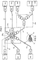
- a multiplex circuit arrangement comprises a plurality of consumer stations VS1-VS8 each comprising a hardware processor for fast serial data exchange (CAN), which are connected to a central bus distributor arrangement ZVA via lines L1-L6.
- a hardware microprocessor e.g. in the magazine "Electronics Information" 3, 88, pages 46 f.f., described in more detail.
- Bus coupling networks are provided at the ends of the lines L1-L8, namely on the side of the consumer stations VS1-VS8, station networks SN1-SN8 and on the part of the central distributor arrangement ZVA distribution networks VN1-VN9.
- the station networks SN and the distribution networks VN which are used as bus coupling networks, are constructed analogously.
- the distribution networks VN7 - VN9 are combined as a sub-distribution arrangement UVA, which can, for example, provide the signal-load distribution in the rear of a motor vehicle.
- FIG. 1 shows a star-shaped network structure in which the star node comprising the distributor networks VN1-VN6 can be arranged in a small spatial area, for example on a circuit board.
- the load lines L L are secured with ring lines 1 and 2 via fuse fuses S1-S6, which are accommodated in a central fuse box 4, before their confluence with the star cross point.
- Each of the lines L1-L8 is designed as a two-wire cable shown in section in FIG. 3, comprising a load line L L with a larger cross section and a data line L D with a smaller cross section.
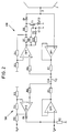
- Each station network SN or distributor network VN shown in detail in FIGS. 2 and 4 comprises two analog amplifiers OP1 and OP2 connected in opposite directions.
- the output of the analog amplifier OP1 is followed by an output resistor R1, the other side of which is connected to the input (+) of the analog amplifier OP2 via a resistor R6.
- the input (-) of the analog amplifier OP2 is connected to ground via a resistor R5 and to the output of the analog amplifier OP2 via a resistor R4 or to the output R x to the consumer station VS via a further resistor R3.
- the input (-) of the analog amplifier OP1 is directly connected to the output.
- the input (+) is connected to ground via a resistor R2 and to the output via a diode D1 switched in the reverse direction of the analog amplifier OP2 and connected to the input T x to the consumer station VS.
- the distribution networks VN provide that two resistors R7, R8 connected in series are provided on the output side of the analog amplifier OP2 between its output and the diode D1, between which the line is connected the input (-) of the analog amplifier OP2 opens via the resistor R4, a transistor T1 being provided, which is connected to ground via the collector-emitter path between the resistor R8 and the diode D1 on the one hand and via a light-emitting diode D3 on the other hand, and the latter Base is connected on the one hand via the resistor R9 and on the other hand via the resistor R1o and the diode D2 to the output of the analog amplifier 2 and via a capacitor C1 to ground.
- connection to the ring line 2 of the star point is via a line 3, which opens between the diode D1 and the input (+) of the amplifier OP1.
- the data line L D opens at the free end of the resistor R1 or R6.
- the resistors R7 - R1o and the capacitor C1 form an RC element which defines the switching point of the transistor T1.
- the circuit arrangement according to the invention works as follows:
- the loop gain of the circuit T x -OP1-R1-R6-OP2-D1 is less than 1.
- the transmit output Tx of the consumer station VS or the hardware processor provided there has an open-drain circuit (open collector).
- the diode D1 provides a so-called "wired-or structure" of the network, i.e. only the high level (dominant bit) is actively coupled in.
- the gain factor of the analog amplifier OP2 counteracts an excessive damping by the diode D1, so that a loop gain of just under 1 can be set, which is required.
- the sending process is as follows:
- a high-level 5V is applied via the open-drain output T x .
- the signal From the output of the analog amplifier OP1 (impedance converter), the signal passes through the matching resistor R1 to the data line L D and at the same time back via the analog amplifier OP2 to the receiver input Rx. If the output Tx sends a low signal, ie if Tx becomes high-resistance, the voltage in the network also breaks down (loop gain ⁇ 1).
- the receiving process works as follows:
- each distribution network VN works accordingly. I.e. starting from the output Tx and via the analog amplifier OP1, the signal reaches the distribution network VN, which works as a receiver and couples the signal into line 2 in the core area of the star structure. All other distribution networks VN of the central distribution arrangement ZVA then act as transmitters and forward the signal to the other consumer stations VS. There the respective station networks SN again act as receivers.
- a low-impedance impedance converter Ra smaller than 10 ohms is provided on both sides of the data line L D , which together with the resistor R1 ensures an exact adjustment.
- the diode D1 in the distribution network VN blocks each ground signal from the associated branch line L from the rest of the bus system.
- the circuit part formed by the resistors R7-R1o, the capacitor C1, the diode D2, the transistor T1 and the diode D1 is provided in the distribution networks VN.
- This circuit part works in such a way that a steady high signal at the anode of diode D1, caused by a short circuit in the data line L D to plus, a defective analog amplifier or a destroyed hardware processor (CAN) would render the bus system itself inoperative.
- the transistor T1 now counteracts this with the aid of the integrator, comprising the resistor R9 and the capacitor C1.
- the transistor T1 becomes conductive and thus shorts the static high signal to ground. Decoupled by diode D1, the rest of the bus system can continue to work undisturbed.
- the combination of the resistor R1o with the diode D2 ensures a quick connection of the branch, if one such an error occurs only briefly. In the event of such a fault, the resistors R7 and R8 protect the analog amplifier OP2 against overload and counteract a tendency to oscillate.
- a circuit arrangement described above is preferably operated so that a start-stop mode is provided, i.e. the bus system is to be switched off in the parked state and started again when any vehicle function is actuated.
- FIG. 4 shows the circuit arrangement described in greater detail above in connection with FIG. 2:
- the voltage level for the low signal is raised to 1.5 V. This voltage is monitored via resistor R17 by transistor T3. The transistor T2 is turned on by the transistor T3, and thus the network is supplied with current.
- Each consumer station VS can wake up the entire bus system again with a start command.
- the own network is first switched on via the diode D5 and the resistor R13, and a high signal is emitted practically simultaneously via the diode D4 and the resistor R12. This signal starts the power supply of the central distributor arrangement ZVA via the resistor R11, is then forwarded to all other consumer stations VS and causes the start of all stations via the resistor R17.
Landscapes
- Engineering & Computer Science (AREA)
- Mechanical Engineering (AREA)
- Computer Networks & Wireless Communication (AREA)
- Signal Processing (AREA)
- Small-Scale Networks (AREA)
- Selective Calling Equipment (AREA)
Abstract
Claims (7)
- Circuit multiplex, notamment pour la commande des postes utilisateurs de véhicules automobiles, chaque poste ayant un processeur câblé pour l'échange rapide en série de données (CAN) et un circuit d'entraînement, avec un système de bus travaillant avec un niveau actif et un niveau passif, les différents postes étant reliés par une structure de réseau, notamment une structure en étoile, circuit caractérisé en ce que chaque ligne de données (LD) possède à une extrémité, un réseau de bus de couplage bidirectionnel (réseau de station SN ou réseau de distributeur VN) comprenant deux amplificateurs analogiques (OP1, OP2) branchés en opposition, au moins plusieurs réseaux de couplage de bus, centraux, (réseau de distributeur VN) étant regroupés suivant un circuit de distributeur de bus central en étoile (ZVA).
- Circuit multiplex selon la revendication 1, caractérisé en ce que pour les lignes de charge (LL), il y a des fusibles de charge (S) dans le circuit distributeur central (ZVA).
- Circuit multiplex selon la revendication 1, caractérisé en ce que les lignes (L) sont réalisées sous la forme de lignes à deux brins asymétriques vers les différents postes utilisateurs (VS).
- Circuit multiplex selon la revendication 1, caractérisé par au moins un circuit de sous-distribution (UVA) pour la distribution données-charge comprenant plusieurs réseaux distributeurs (VN).
- Circuit multiplex selon la revendication 1, caractérisé par une résistance adaptatrice (R1) branchée sur la sortie du premier amplificateur analogique (OP1) fonctionnant comme convertisseur d'impédance.
- Circuit multiplex selon la revendication 1, caractérisé par une diode constituant un moyen de protection contre les courts-circuits vis-à-vis de la ligne négative, branchée sur la sortie du second amplificateur analogique (OP2).
- Circuit multiplex selon la revendication 1, caractérisé en ce qu'entre la sortie du second amplificateur analogique (OP2) et la diode (D1) il est prévu un circuit de protection contre les courts-circuits vers la ligne positive, circuit comprenant un transistor (T1), une diode (D3), un intégrateur (R7-R10 ; C1) et une diode (D2), le transistor (T1) court-circuitant à la masse un signal statique haut en fonction des constantes de temps de l'intégrateur (R7-R10 ; C1).
Applications Claiming Priority (2)
| Application Number | Priority Date | Filing Date | Title |
|---|---|---|---|
| DE3936894 | 1989-11-06 | ||
| DE3936894A DE3936894A1 (de) | 1989-11-06 | 1989-11-06 | Multiplex-schaltungsanordnung, insbesondere fuer die ansteuerung von verbraucher-stationen in kraftfahrzeugen |
Publications (2)
| Publication Number | Publication Date |
|---|---|
| EP0500557A1 EP0500557A1 (fr) | 1992-09-02 |
| EP0500557B1 true EP0500557B1 (fr) | 1993-12-29 |
Family
ID=6392958
Family Applications (1)
| Application Number | Title | Priority Date | Filing Date |
|---|---|---|---|
| EP90914899A Expired - Lifetime EP0500557B1 (fr) | 1989-11-06 | 1990-10-16 | Circuit multiplex, notamment pour commander des postes consommateurs dans des vehicules a moteur |
Country Status (6)
| Country | Link |
|---|---|
| US (1) | US5313460A (fr) |
| EP (1) | EP0500557B1 (fr) |
| JP (1) | JP3145110B2 (fr) |
| DE (2) | DE3936894A1 (fr) |
| ES (1) | ES2048506T3 (fr) |
| WO (1) | WO1991006447A1 (fr) |
Families Citing this family (20)
| Publication number | Priority date | Publication date | Assignee | Title |
|---|---|---|---|---|
| IT1232090B (it) * | 1989-05-04 | 1992-01-23 | Sgs Thomson Microelectronics | Sistema di collegamento tra un unita di elaborazione principale e del le unita periferiche |
| DE4037143A1 (de) * | 1990-11-22 | 1992-05-27 | Bosch Gmbh Robert | Steuerungssystem |
| JPH07500463A (ja) * | 1991-10-26 | 1995-01-12 | ダイムラークライスラー アクチエンゲゼルシャフト | データ通信システム |
| DE4139300A1 (de) * | 1991-11-29 | 1993-06-03 | Rheydt Kabelwerk Ag | Netzwerk-topologie zur datenuebertragung |
| DE19625401C1 (de) * | 1996-06-25 | 1997-09-18 | Siemens Ag | Bussystem zur Datenübertragung |
| DE19720401A1 (de) * | 1996-09-07 | 1998-03-12 | Bayerische Motoren Werke Ag | Datenbus für mehrere Teilnehmer |
| DE19720398B4 (de) * | 1996-09-07 | 2009-09-24 | Bayerische Motoren Werke Aktiengesellschaft | Datenbus für Fahrzeuge mit mehreren der Insassen-Sicherheit dienenden Einrichtungen |
| US6587474B1 (en) | 1996-09-07 | 2003-07-01 | Bayerische Motoren Werke Aktiengesellschaft | Data bus for multiple components |
| DE19745689A1 (de) * | 1997-10-16 | 1999-04-22 | Bayerische Motoren Werke Ag | Vorrichtung in Fahrzeugen |
| JP4144178B2 (ja) * | 1997-11-14 | 2008-09-03 | アイダブリューエス インターナショナル インコーポレイテッド | インテリジェント電流分配システムおよびその製造方法 |
| FI113420B (fi) * | 1997-11-14 | 2004-04-15 | Iws Internat Inc Oy | Älykäs ohjausjärjestelmä kulkuneuvon virranjakelua varten |
| DE19810292A1 (de) | 1998-03-10 | 1999-09-16 | Bayerische Motoren Werke Ag | Datenbus für mehrere Teilnehmer |
| DE19810290A1 (de) * | 1998-03-10 | 1999-09-16 | Bayerische Motoren Werke Ag | Datenbus für mehrere Teilnehmer |
| US6249060B1 (en) * | 1999-06-18 | 2001-06-19 | Jonathan P. Osha | Multiplexed cabling system for a vehicle |
| DE10028830A1 (de) * | 2000-06-10 | 2001-12-13 | Merten Gmbh & Co Kg | Einrichtung für ein Datenleitungsnetz zum Anschluß eines Gerätes |
| DE10142410A1 (de) | 2001-08-31 | 2003-04-03 | Bosch Gmbh Robert | Versorgungsleitungsstruktur zur Energieversorgung von elektrischen Komponenten eines Kraftfahrzeugs |
| DE10211834A1 (de) * | 2002-03-16 | 2003-09-25 | Philips Intellectual Property | Fahrzeug-Datennetzwerk |
| EP1859989B1 (fr) * | 2006-05-17 | 2016-03-09 | Hobby-Wohnwagenwerk Ing. Harald Striewski GmbH | Installation électrique pour camping-car |
| US7936081B2 (en) * | 2008-01-30 | 2011-05-03 | Caterpillar Inc. | Power converter control system for electric powertrains |
| DE102019219904B4 (de) * | 2019-12-17 | 2022-12-22 | Conti Temic Microelectronic Gmbh | Datennetzwerk mit zumindest drei Leitungszweigen, die über einen gemeinsamen Sternpunkt miteinander verbunden sind, sowie Kraftfahrzeug und Betriebsverfahren für das Datennetzwerk |
Family Cites Families (8)
| Publication number | Priority date | Publication date | Assignee | Title |
|---|---|---|---|---|
| US3697767A (en) * | 1970-02-12 | 1972-10-10 | Carrozzeria Pininfarina Soc Pe | Electric energy distribution systems |
| FR2166696A5 (fr) * | 1972-01-04 | 1973-08-17 | Ass Ouvriers Instr Preci | |
| FR2331913A2 (fr) * | 1972-01-04 | 1977-06-10 | Ass Ouvriers Instr Precision | Dispositif d'emission et de reception d'impulsions telephoniques codees |
| DE3149142A1 (de) * | 1981-12-11 | 1983-06-23 | Wabco Westinghouse Fahrzeugbremsen GmbH, 3000 Hannover | Multiplex-verkabelungssystem fuer fahrzeuge |
| FR2549617B1 (fr) * | 1983-07-20 | 1986-02-07 | Citroen Sa | Perfectionnements apportes aux installations pour la commande et/ou le controle des consommateurs d'energie electrique de vehicules |
| US4897834A (en) * | 1987-08-18 | 1990-01-30 | Allen-Bradley Company, Inc. | Bit oriented communications network |
| DE3730468A1 (de) * | 1987-09-08 | 1989-03-16 | Bergmann Kabelwerke Ag | Bordnetz fuer kraftfahrzeuge und verfahren zum betrieb des bordnetzes |
| US4845708A (en) * | 1987-10-09 | 1989-07-04 | Amp Incorporated | Vehicle multiplex system |
-
1989
- 1989-11-06 DE DE3936894A patent/DE3936894A1/de not_active Withdrawn
-
1990
- 1990-10-16 WO PCT/DE1990/000784 patent/WO1991006447A1/fr active IP Right Grant
- 1990-10-16 ES ES90914899T patent/ES2048506T3/es not_active Expired - Lifetime
- 1990-10-16 JP JP51387490A patent/JP3145110B2/ja not_active Expired - Lifetime
- 1990-10-16 US US07/839,771 patent/US5313460A/en not_active Expired - Fee Related
- 1990-10-16 EP EP90914899A patent/EP0500557B1/fr not_active Expired - Lifetime
- 1990-10-16 DE DE90914899T patent/DE59004055D1/de not_active Expired - Fee Related
Also Published As
| Publication number | Publication date |
|---|---|
| JPH05501640A (ja) | 1993-03-25 |
| EP0500557A1 (fr) | 1992-09-02 |
| JP3145110B2 (ja) | 2001-03-12 |
| WO1991006447A1 (fr) | 1991-05-16 |
| US5313460A (en) | 1994-05-17 |
| DE59004055D1 (de) | 1994-02-10 |
| ES2048506T3 (es) | 1994-03-16 |
| DE3936894A1 (de) | 1991-05-08 |
Similar Documents
| Publication | Publication Date | Title |
|---|---|---|
| EP0500557B1 (fr) | Circuit multiplex, notamment pour commander des postes consommateurs dans des vehicules a moteur | |
| EP1401158B1 (fr) | Dispositif de couplage pour un système de bus sériel | |
| EP3024705B1 (fr) | Module interrupteur pour séparer des composants d'un circuit multitensions de véhicule | |
| DE4229175A1 (de) | Netzwerkschnittstelle | |
| WO1990009713A1 (fr) | Interface de reseau | |
| DE19611942A1 (de) | Halbleiterschaltkreis für ein elektronisches Steuergerät | |
| DE102010049835A1 (de) | Netzwerk und Verfahren zum Betreiben eines Netzwerks | |
| EP0661849B1 (fr) | Système de bus de données | |
| DE69412680T2 (de) | Treiberschaltung für die Bus-Schaltung eines Kraftfahrzeug-Multiplex-Kommunikationssystems | |
| EP1085705B1 (fr) | Réseau avec plusiers noeuds et au moins un noeud central | |
| EP0643515B1 (fr) | Dispositif pour la transmission bidirectionnelle de données | |
| DE112020003704T5 (de) | Elektronische Steuervorrichtung und Fehlererfassungsverfahren | |
| DE102010044892A1 (de) | Gefahrenmeldeanlage mit zwei Datenübertragungsgeschwindigkeiten | |
| DE102013214953A1 (de) | Anordnung zum Anschluss einer Komponente an ein Master- Steuergerät eines Kraftfahrzeugs | |
| DE102010049834A1 (de) | Netzwerk und Verfahren zum Betreiben eines Netzwerks | |
| EP1589437A2 (fr) | Circuit d'interface électronique et système de bus avec un tel circuit d'interface | |
| EP1236306B1 (fr) | Systeme de bus | |
| DE69132259T2 (de) | Vorrichtung zur spannungseinstellung in einem multiplexübertragungssystem | |
| WO1990008437A2 (fr) | Raccordement de postes a des bus | |
| EP1143668B1 (fr) | Solution des conflits d'acces aux supports dans des réseaux avec plusieurs noeuds et au moins un noed central | |
| DE19813952C1 (de) | Signalisierungsendstufe zur Erzeugung digitaler Spannungssignale auf einem Bussystem | |
| DE102014221672A1 (de) | Steuergerät für ein Mehrspannungsbordnetz | |
| EP2254011B1 (fr) | Alimentation en énergie d'une interface AS | |
| DE69120054T2 (de) | Ausgabeverwaltungskreis für speicherprogrammierbare steuerung | |
| DE10133441C2 (de) | Schaltungsanordnung zur Spannungssymmetrierung von Datenbussen |
Legal Events
| Date | Code | Title | Description |
|---|---|---|---|
| PUAI | Public reference made under article 153(3) epc to a published international application that has entered the european phase |
Free format text: ORIGINAL CODE: 0009012 |
|
| 17P | Request for examination filed |
Effective date: 19920328 |
|
| AK | Designated contracting states |
Kind code of ref document: A1 Designated state(s): DE ES FR GB IT SE |
|
| 17Q | First examination report despatched |
Effective date: 19930521 |
|
| GRAA | (expected) grant |
Free format text: ORIGINAL CODE: 0009210 |
|
| AK | Designated contracting states |
Kind code of ref document: B1 Designated state(s): DE ES FR GB IT SE |
|
| ET | Fr: translation filed | ||
| GBT | Gb: translation of ep patent filed (gb section 77(6)(a)/1977) |
Effective date: 19940111 |
|
| REF | Corresponds to: |
Ref document number: 59004055 Country of ref document: DE Date of ref document: 19940210 |
|
| REG | Reference to a national code |
Ref country code: ES Ref legal event code: FG2A Ref document number: 2048506 Country of ref document: ES Kind code of ref document: T3 |
|
| ITF | It: translation for a ep patent filed | ||
| PLBE | No opposition filed within time limit |
Free format text: ORIGINAL CODE: 0009261 |
|
| STAA | Information on the status of an ep patent application or granted ep patent |
Free format text: STATUS: NO OPPOSITION FILED WITHIN TIME LIMIT |
|
| 26N | No opposition filed | ||
| EAL | Se: european patent in force in sweden |
Ref document number: 90914899.1 |
|
| PGFP | Annual fee paid to national office [announced via postgrant information from national office to epo] |
Ref country code: DE Payment date: 19961213 Year of fee payment: 7 |
|
| REG | Reference to a national code |
Ref country code: GB Ref legal event code: 746 Effective date: 19961128 |
|
| REG | Reference to a national code |
Ref country code: FR Ref legal event code: D6 |
|
| PGFP | Annual fee paid to national office [announced via postgrant information from national office to epo] |
Ref country code: GB Payment date: 19971010 Year of fee payment: 8 |
|
| PGFP | Annual fee paid to national office [announced via postgrant information from national office to epo] |
Ref country code: SE Payment date: 19971027 Year of fee payment: 8 Ref country code: FR Payment date: 19971027 Year of fee payment: 8 |
|
| PGFP | Annual fee paid to national office [announced via postgrant information from national office to epo] |
Ref country code: ES Payment date: 19971031 Year of fee payment: 8 |
|
| PG25 | Lapsed in a contracting state [announced via postgrant information from national office to epo] |
Ref country code: DE Free format text: LAPSE BECAUSE OF NON-PAYMENT OF DUE FEES Effective date: 19980701 |
|
| PG25 | Lapsed in a contracting state [announced via postgrant information from national office to epo] |
Ref country code: GB Free format text: LAPSE BECAUSE OF NON-PAYMENT OF DUE FEES Effective date: 19981016 |
|
| PG25 | Lapsed in a contracting state [announced via postgrant information from national office to epo] |
Ref country code: SE Free format text: LAPSE BECAUSE OF NON-PAYMENT OF DUE FEES Effective date: 19981017 Ref country code: ES Free format text: LAPSE BECAUSE OF THE APPLICANT RENOUNCES Effective date: 19981017 |
|
| GBPC | Gb: european patent ceased through non-payment of renewal fee |
Effective date: 19981016 |
|
| EUG | Se: european patent has lapsed |
Ref document number: 90914899.1 |
|
| PG25 | Lapsed in a contracting state [announced via postgrant information from national office to epo] |
Ref country code: FR Free format text: LAPSE BECAUSE OF NON-PAYMENT OF DUE FEES Effective date: 19990630 |
|
| REG | Reference to a national code |
Ref country code: FR Ref legal event code: ST |
|
| REG | Reference to a national code |
Ref country code: ES Ref legal event code: FD2A Effective date: 20001009 |
|
| PG25 | Lapsed in a contracting state [announced via postgrant information from national office to epo] |
Ref country code: IT Free format text: LAPSE BECAUSE OF NON-PAYMENT OF DUE FEES;WARNING: LAPSES OF ITALIAN PATENTS WITH EFFECTIVE DATE BEFORE 2007 MAY HAVE OCCURRED AT ANY TIME BEFORE 2007. THE CORRECT EFFECTIVE DATE MAY BE DIFFERENT FROM THE ONE RECORDED. Effective date: 20051016 |