EP0497433B1 - Phasengesteuerte Demodulationseinrichtung zur digitalen Kommunikation - Google Patents
Phasengesteuerte Demodulationseinrichtung zur digitalen Kommunikation Download PDFInfo
- Publication number
- EP0497433B1 EP0497433B1 EP92201171A EP92201171A EP0497433B1 EP 0497433 B1 EP0497433 B1 EP 0497433B1 EP 92201171 A EP92201171 A EP 92201171A EP 92201171 A EP92201171 A EP 92201171A EP 0497433 B1 EP0497433 B1 EP 0497433B1
- Authority
- EP
- European Patent Office
- Prior art keywords
- carrier
- output
- circuit
- ratio
- digital
- Prior art date
- Legal status (The legal status is an assumption and is not a legal conclusion. Google has not performed a legal analysis and makes no representation as to the accuracy of the status listed.)
- Expired - Lifetime
Links
Images


Classifications
-
- H—ELECTRICITY
- H04—ELECTRIC COMMUNICATION TECHNIQUE
- H04L—TRANSMISSION OF DIGITAL INFORMATION, e.g. TELEGRAPHIC COMMUNICATION
- H04L27/00—Modulated-carrier systems
- H04L27/18—Phase-modulated carrier systems, i.e. using phase-shift keying
- H04L27/22—Demodulator circuits; Receiver circuits
- H04L27/227—Demodulator circuits; Receiver circuits using coherent demodulation
- H04L27/2271—Demodulator circuits; Receiver circuits using coherent demodulation wherein the carrier recovery circuit uses only the demodulated signals
- H04L27/2273—Demodulator circuits; Receiver circuits using coherent demodulation wherein the carrier recovery circuit uses only the demodulated signals associated with quadrature demodulation, e.g. Costas loop
-
- G—PHYSICS
- G01—MEASURING; TESTING
- G01R—MEASURING ELECTRIC VARIABLES; MEASURING MAGNETIC VARIABLES
- G01R29/00—Arrangements for measuring or indicating electric quantities not covered by groups G01R19/00 - G01R27/00
- G01R29/26—Measuring noise figure; Measuring signal-to-noise ratio
-
- H—ELECTRICITY
- H04—ELECTRIC COMMUNICATION TECHNIQUE
- H04B—TRANSMISSION
- H04B17/00—Monitoring; Testing
- H04B17/20—Monitoring; Testing of receivers
-
- H—ELECTRICITY
- H04—ELECTRIC COMMUNICATION TECHNIQUE
- H04L—TRANSMISSION OF DIGITAL INFORMATION, e.g. TELEGRAPHIC COMMUNICATION
- H04L27/00—Modulated-carrier systems
- H04L27/0014—Carrier regulation
- H04L2027/0016—Stabilisation of local oscillators
-
- H—ELECTRICITY
- H04—ELECTRIC COMMUNICATION TECHNIQUE
- H04L—TRANSMISSION OF DIGITAL INFORMATION, e.g. TELEGRAPHIC COMMUNICATION
- H04L27/00—Modulated-carrier systems
- H04L27/0014—Carrier regulation
- H04L2027/0044—Control loops for carrier regulation
- H04L2027/0063—Elements of loops
- H04L2027/0067—Phase error detectors
-
- H—ELECTRICITY
- H04—ELECTRIC COMMUNICATION TECHNIQUE
- H04L—TRANSMISSION OF DIGITAL INFORMATION, e.g. TELEGRAPHIC COMMUNICATION
- H04L27/00—Modulated-carrier systems
- H04L27/0014—Carrier regulation
- H04L2027/0044—Control loops for carrier regulation
- H04L2027/0071—Control of loops
- H04L2027/0075—Error weighting
Definitions
- the present invention relates to a phase controlled demodulator system for digital communication.
- a phase controlled demodulation system for digital communication comprising a quadrature detector for receiving a digital signal modulated upon a transmitted carrier and generating therefrom I-channel and Q-channel signals, a voltage controlled oscillator for generating a local carrier as a replica of the transmitted carrier and applying said local carrier to said quadrature detector, and a phase difference detection and filter circuit for detecting the phase difference between said I-channel and Q-channel signals for controlling said voltage controlled oscillator, characterized by carrier-to-noise ratio detector means for detecting the carrier-to-noise ratio of one of said I-channel and Q-channel signals, and means for detecting the ratio difference between the detected carrier-to-noise ratio and a predetermined value, and in that said voltage controlled oscillator is further controlled by the detected ratio difference so as to tend to maintain the carrier-to-noise ratio at a maximum value.
- the C/N ratio is therefore a determining factor for system evaluation.
- the evaluation of a satellite channel is made by inserting a band-pass filter having a passband narrower than the bandwidth of the satellite transponder at the input of a demodulator.
- a test carrier having a frequency corresponding to the center frequency of the band-pass filter is transmitted to measure the level of power at the output of the filter which represents the total value (C + N).
- the carrier is then removed and the power level is again measured as a representation of the noise component N.
- the carrier component C is then obtained by subtracting the noise N from the total value (C + N) and finally the value C is divided by the noise value N to obtain the ratio C/N.
- the equivalent noise bandwidth of the band-pass filter corresponds to the constant B.
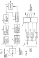
- a C/N ratio detector which comprises an analog-to-digital converter 1 connected to receive a demodulated 2-PSK signal from a demodulator, not shown, and driven at a clock rate used to recover symbols by the demodulator for sampling the demodulated signal at the recovered symbol rate.
- An absolute value circuit 2 is connected to the output of the A/D converter to convert the negative value of the digital output to a positive value and supplies an absolute value signal to a first averaging circuit 3 the output of which is connected to a first squaring circuit 4 to produce an output representing the carrier component value C.
- A/D converter 1 is further applied to a second squaring circuit 5 to which a second averaging circuit 6 is connected to produce an output representing the total component value (C + N).
- a subtractor 7 is connected to the outputs of the circuits 4 and 6 to subtract the output of squaring circuit 4 from the output of averaging circuit 6 to obtain the noise component value N.
- a division circuit 8 is connected to the output of squaring circuit 4 and to the output of the subtractor 7 to determine the ratio C/N.
- the output of the demodulator is an analog signal having eye patterns at the recovery timing of symbols which corresponds to signal points.
- Absolute value circuit 2 converts the data d i into an absolute value
- MSB most significant bit
- the polarity inverter 12 inverts the logic state of the input of each exclusive OR gate when the MSB is at logic 1 and applies the inverted bits to adder 13, while it passes the inputs of all the exclusive OR gates to adder 13 without altering their logic states when the MSB is at logic 0 .
- Adder 13 adds MSB of the 3-bit inputs from A/D converter 1 to the least significant bit (LSB) of the 3-bit inputs from the polarity inverter 12 and produces 4-bit outputs. As a result, absolute values shown in Table 2 are derived.
- Averaging circuit 3 averages the absolute values for a period of N symbols which is sufficiently long to suppress short term variations and applies an average value to squaring circuit 4.
- averaging circuit 3 comprises an adder 14 connected to the output of averaging circuit 2, a one-sample delay 15 which is reset at N-symbol intervals and connected between the output of the adder 14 and a second input of the adder 14.
- Adder 14 and delay 15 form an integrator for integrating N symbols which is divided by a division circuit 16 by a constant N.
- the noise component contained in digital data has a Gaussian distribution centered on an amplitude A at zero noise level, the noise component is cancelled out by the averaging process just described, and therefore, the output of averaging circuit 3 gives the amplitude of a signal point of the demodulated signal under noiseless conditions and is represented by Equation (1).
- the output of A/D converter 1 is squared by second squaring circuit 5 and averaged over N symbols by the second averaging circuit 6 in a manner similar to the processes performed by averaging circuit 3 and squaring circuit 4 just described.
- the first term of Equation (4) can be obtained at the output of averaging circuit 6, namely, ⁇ 2 + A 2.
- Subtractor 7 subtracts the signal power A 2 at the output of squaring circuit 4 from the ( ⁇ 2 + A 2) output of averaging circuit 6 to derive a noise power ⁇ 2 which is used by division circuit 8 to divide the output A 2 of squaring circuit 4.
- division circuit 8 comprises a conversion table, or a read only memory 17.
- a set of values S / ⁇ 2 are stored in cell locations addressable as a function of variables S and ⁇ 2.
- the first embodiment is not suited for systems severely affected by noise.
- the probability density distribution of a received 2-PSK signal adopts a curve 40 which is a Gaussian distribution under low noise conditions.
- the polarity inversion of the negative values by absolute value circuit 2 causes the signal point with amplitude - A to be folded over to the signal point with amplitude A , while maintaining the symmetry of the curve 40.
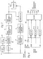
- a second carrier to noise ratio detector is shown in Fig.7.
- This embodiment eliminates the disadvantage of the first detector by taking advantage of the forward error coding and decoding techniques employed in digital transmission systems.
- the second detector includes a delay 20 connected to the output of A/D converter 1, an FEC (forward error correcting) decoder 21 for decoding the output of A/D converter 1 and correcting errors and feeding an FEC encoder 22.
- the output of encoder 22 is connected to one input of a polarity inverter 23 to which the output of delay 20 is also applied.
- Polarity inverter 23 supplies a decision threshold to the first averaging circuit 3.
- FEC decoder 21 performs error decoding operation on the output of A/D converter 1 by correcting errors according to a known error correcting to application to the FEC encoder of a transmitter, not shown. This signal is applied to FEC encoder 22 in the same way as the transmitter's FEC encoder. With the error decoding and encoding processes, the output of FEC encoder 22 can be considered more akin to the output of the transmitter's FEC encoder than the output of the receiver's demodulator is to it. Therefore, a binary 1 at the output of encoder 22 indicates that the received input signal is at a signal point having an amplitude A in a probability density distribution of amplitudes (Fig. 5) and a binary 0 at the encoder output indicates that the input signal is at a signal point with an amplitude- A .
- A/D converter 1 The output of A/D converter 1 is delayed by circuit 20 by an amount equal to the total delay introduced by decoder 21 and encoder 22 so that the inputs to the polarity inverter 23 are rendered time-coincident with each other.
- Polarity inverter 23 uses the output of FEC encoder 22 as a criterion to determine whether the output of the delay 20 lies at a signal point having an amplitude A or at a signal point having an amplitude - A .
- polarity inverter 23 applies the output from delay 20 without altering its polarity to averaging circuit 3 and in response to a binary 0 , it applies the output of delay 20 to averaging circuit 3 by inverting its polarity.
- polarity inverter 23 comprises a NOT circuit 30 connected to the output of FEC encoder 22, exclusive OR gates 31- 1 to 31- n , and an adder 32.
- Each exclusive OR gate 31 has a first input terminal connected to the output of the NOT circuit 30 and a second input terminal connected to a respective one of the n outputs of the delay circuit 20. Since the output of delay 20 is represented by 2's complements of the n -bit data, binary 0 at the output of encoder 22 causes the logic states of the outputs of delay 20 to be inverted by exclusive OR gates 31- 1 through 31- n and summed with a binary 1 from inverter 30 which is summed by adder 32 with the LSB of the n-bit outputs from exclusive OR gates 31, while a binary 1 at the output of encoder 22 causes the delay 20 outputs to pass through gates 31 to adder 32 without undergoing polarity inversion.
- the probability density distribution of the demodulated signal is centered on the signal point having amplitude A and adopts the curve 40 of Fig.5 and the average value of the amplitudes of the received signal rendered equal to the amplitude at the signal point with amplitude A .
- the output of the first squaring circuit 4 can be expressed by the following equation: where, SGN ( d i ) represents the criterion data from FEC encoder 22.
- Fig. 9 is a graphic representation of the relationship between the E b /N o values obtained by circuit of Fig.7 and theoretical E b /N o values. As is apparent, there is a complete agreement between the measured and theoretical values down to low E b /N o input values. This indicates that C/N ratio can be precisely determined even if the transmission system suffers severe noise.
- Measurement of C/N ratio of a system without interrupting its service can also be effected alternatively by a third carrier to noise detector shown in Fig. 10. This detector differs from the first detector by the inclusion of a adaptive weighting circuit 50.
- the absolute value of the output of A/D converter 1 is taken by absolute value circuit 2 and weighted with a prescribed weighting factor by the adaptive weighting circuit 50.
- the output signal of the adaptive weighting circuit 50 is applied to the first averaging circuit 3 where short term variations, i.e., noise component N ( t ) are removed to produce an output
- W ( u ) ⁇ , where W ( u ) represents the weighting factor, and u
- This weighting factor is determined so that the adverse fold-over effect produced by taking the absolute values is minimized.
- the following conditions are examples of weighting factor in which the value x represents the output of the absolute value circuit 2 and TH is a threshold value.
- Fig. 11 is one example of the adaptive weighting circuit 50 which is constructed according to the condition (3).
- Weighting circuit 50 comprises a comparator 51, a multiplier 52 and a selector 53 to which the outputs of absolute circuit 2 and multiplier 52 are applied to be selectively coupled to the division circuit 8.
- Comparator 51 compares between the output of the absolute value circuit 2 and a threshold value TH and applies a logic selection signal to the selector 53. If the output of absolute value circuit 2 is higher than threshold value TH , the selection signal is at logic 1 and if otherwise, the selection signal is at logic 0.
- Multiplier 52 multiplies the weighting factor - ⁇ on the output of the absolute value circuit 2 and applies it to selector 53. If the comparator 51 output is at logic 1 , the output of absolute value circuit 2 is passed through the selector 52 to the averaging circuit 3 and if otherwise, the output of multiplier 52 is passed to the averaging circuit 3.
- the probability density distribution of the amplitudes of input signal adopts a curve shown at D in Fig. 12b which is shifted to the right from the position of curve C (Fig. 12a) by an amount equal to the distance between the intermediate point 0 and the threshold value TH .
- the weighting factor - ⁇ is so determined that the noise component which would otherwise cause the most serious fold-over effect is reduced to a minimum.
- Subtractor 7 performs the following subtraction S ( t )2 ⁇ + N ( t )2 ⁇ - S ( t ) ⁇ W ( u ) ⁇ 2 to produce an output which represents N ( t )2 ⁇ , which is applied to the division circuit 8.
- the division circuit 8 comprises a conversion table to which the signals N ( t )2 ⁇ and S ( t )2 ⁇ + N ( t )2 ⁇ are applied as address signals.
- Fig. 13 is a graphic representation of the characteristic of the third embodiment using a threshold value 0.25, and a weighting factor -0.5. Comparison between Figs. 6 and 13 indicates that precision of the circuit is improved by as much as 4 dB at high noise levels (low E b /N o inputs).
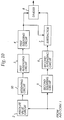
- the C/N ratio of a demodulator output is found to vary with a deviation of the frequency of the carrier recovered by the demodulator from the frequency of the received carrier.
- the carrier-to-noise ratio detector illustrated can therefore be used instead of the costly automatic frequency control circuit for preventing the demodulator from being locked in a pseudo-sync state. This is accomplished by controlling a voltage controlled oscillator provided in a closed loop of the demodulator in accordance with the derived C/N ratio such that the latter is maintained at a maximum level.
- a demodulator 60 includes a quadrature detector 61 which receives an input PSK signal at terminal 64 and a recovered carrier from a voltage controlled oscillator 62 and produces demodulated signals at terminals 65.
- the demodulated output signals are applied to a phase detection and filtering circuit 63 to control the VCO 62 in accordance with a phase difference detected between the two output signals.
- One of the output signals is applied to the input of the C/N ratio detector which is identical to that shown in Fig. 1.
- the output of the division circuit 8 of the C/N ratio detector is applied to a controller 66 including a differential amplifier for comparison with a reference threshold.
- This reference threshold corresponds to a DC voltage at which the VCO 62 generates a carrier at the desired frequency when the C/N ratio of the demodulator 60 is at a maxaimum value.
- the output of the differential amplifier 66 is representative of the deviation of the C/N ratio from its maximum value and is applied to the control terminal of the VCO 62.
- the C/N ratio of the demodulator is at the maximum value.
- the noise component increases in the outputs of the demodulator 60 and hence the C/N ratio of the demodulator decreases, causing the output of the differential amplifier 66 to vary correspondingly.
- the VCO frequency is controlled until the output of the division circuit 8 returns to the maximum value of the C/N ratio.
Claims (2)
- Phasengesteuerte Demodulationseinrichtung zur digitalen Kommunikation mit einem Quadraturdetektor (61) zum Empfangen eines auf einem übertragenen Träger modulierten digitalen Signals und zum Erzeugen von I-Kanal- und Q-Kanal-Signalen daraus, einem spannungsgesteuerten Oszillator (62) zum Erzeugen eines lokalen Trägers als eine Kopie des übertragenen Trägers und zum Anlegen des lokalen Trägers an den Quadraturdetektor (61), und eine Phasendifferenz-Detektions- und Filterschaltung (63) zum Detektieren der Phasendifferenz zwischen dem I-Kanal- und dem Q-Kanal-Signal, um den spannungsgesteuerten Oszillator zu steuern, gekennzeichnet durch eine Träger/Rausch-Verhältnis-Detektionseinrichtung (1 bis 8) zum Detektieren des Träger/Rausch-Verhältnisses von einem von den I-Kanal- und Q-Kanal-Signalen, und eine Einrichtung (66) zum Detektieren der Verhältnisdifferenz zwischen dem detektierten Träger/Rausch-Verhältnis und einem vorgegebenen Wert, und dadurch, daß der spannungsgesteuerte Oszillator ferner durch die detektierte Verhältnisdifferenz gesteuert wird, um so das Träger/Rausch-Verhältnis auf einem maximalem Wert zu halten zu versuchen.
- Phasengesteuerte Demodulationseinrichtung nach Anspruch 1, wobei die Träger/Rausch-Verhältnis-Detektionseinrichtung einen Analog/Digital-Wandler (1) zum Abtasten eines von den demodulierten I- und Q-Signalen bei einer Symboltaktrate und zum Umwandeln des abgetasteten Signals in ein digitales Ausgangssignal mit positiven und negativen Werten, eine Absolutwert-Wandlereinrichtung (2) zum Umwandeln des digitalen Ausgangssignals aus dem Analog/ Digital-Wandler in ein digitales Absolutwertsignal, eine erste Mittelungseinrichtung (3) zum Mitteln des digitalen Absolutwertsignals über eine Periode einer Anzahl von Symbolen, die ausreicht, um kurzzeitige Schwankungen zu unterdrücken, eine erste Quadrierungseinrichtung (4) zum Quadrieren des Wertes des digitalen Absolutwertsignals aus der ersten Mittelungseinrichtung, eine zweite Quadrierungseinrichtung (5) zum Quadrieren des Wertes des digitalen Signals aus dem Analog/Digital-Wandler, eine zweite Mittelungseinrichtung (6) zum Mitteln des quadrierten digitalen Signals aus der zweiten Quadrierungseinrichtung, um kurzzeitige Schwankungen zu unterdrücken, eine Einrichtung (7) zum Subtrahieren des quadrierten digitalen Ausgangssignals aus der ersten Quadrierungseinrichtung von dem gemittelten digitalen Ausgangssignal der zweiten Mittelungseinrichtung, und eine Einrichtung (8) zum Ableiten des Verhältnisses zwischen dem Ausgangssignal der ersten Quadrierungseinrichtung (4) und dem Ausgangssignal der Subtraktionseinrichtung (7) als das Träger/Rausch-Verhältnis und zum Anlegen des so abgeleiteten Verhältnisses an die Verhältnisdifferenz-Detektionseinrichtung (66) aufweist.
Applications Claiming Priority (9)
| Application Number | Priority Date | Filing Date | Title |
|---|---|---|---|
| JP156045/87 | 1987-06-23 | ||
| JP62-156044A JPH01843A (ja) | 1987-06-23 | C/n測定回路 | |
| JP156044/87 | 1987-06-23 | ||
| JP15604587A JPS64844A (en) | 1987-06-23 | 1987-06-23 | C/n measuring circuit |
| JP16210987A JPS645248A (en) | 1987-06-29 | 1987-06-29 | C/n measuring circuit |
| JP162109/87 | 1987-06-29 | ||
| JP62175658A JPS6418339A (en) | 1987-07-14 | 1987-07-14 | Pseudo synchronizing detecting circuit |
| JP175658/87 | 1987-07-14 | ||
| EP88305685A EP0296822B1 (de) | 1987-06-23 | 1988-06-22 | Träger/Rausch-Detektor für digitale Übertragungssysteme |
Related Parent Applications (1)
| Application Number | Title | Priority Date | Filing Date |
|---|---|---|---|
| EP88305685.5 Division | 1988-06-22 |
Publications (3)
| Publication Number | Publication Date |
|---|---|
| EP0497433A2 EP0497433A2 (de) | 1992-08-05 |
| EP0497433A3 EP0497433A3 (en) | 1992-09-23 |
| EP0497433B1 true EP0497433B1 (de) | 1995-09-20 |
Family
ID=27473388
Family Applications (2)
| Application Number | Title | Priority Date | Filing Date |
|---|---|---|---|
| EP92201171A Expired - Lifetime EP0497433B1 (de) | 1987-06-23 | 1988-06-22 | Phasengesteuerte Demodulationseinrichtung zur digitalen Kommunikation |
| EP88305685A Expired - Lifetime EP0296822B1 (de) | 1987-06-23 | 1988-06-22 | Träger/Rausch-Detektor für digitale Übertragungssysteme |
Family Applications After (1)
| Application Number | Title | Priority Date | Filing Date |
|---|---|---|---|
| EP88305685A Expired - Lifetime EP0296822B1 (de) | 1987-06-23 | 1988-06-22 | Träger/Rausch-Detektor für digitale Übertragungssysteme |
Country Status (5)
| Country | Link |
|---|---|
| US (1) | US4835790A (de) |
| EP (2) | EP0497433B1 (de) |
| AU (1) | AU594621B2 (de) |
| CA (1) | CA1332450C (de) |
| DE (2) | DE3886107T2 (de) |
Families Citing this family (68)
| Publication number | Priority date | Publication date | Assignee | Title |
|---|---|---|---|---|
| JPH0748750B2 (ja) * | 1988-11-15 | 1995-05-24 | 日本電気株式会社 | 同期復調装置 |
| FR2645373A1 (fr) * | 1989-03-28 | 1990-10-05 | Js Telecommunications | Procede et dispositif de reduction du bruit sur un signal codable a plusieurs niveaux predetermines |
| FR2661580B1 (fr) * | 1990-04-27 | 1992-06-12 | Alcatel Transmission | Procede de recuperation de porteuse pour modulation a grand nombre d'etats et dispositif de mise en óoeuvre de ce procede. |
| US5208835A (en) * | 1990-09-24 | 1993-05-04 | In-Situ, Inc. | Automatic frequency control system and method for frequency-shift-key data transmission systems |
| US5341402A (en) * | 1991-02-19 | 1994-08-23 | Tokyo Electric Co., Ltd. | Automatic frequency control method and device for use in receiver |
| WO1992021984A1 (en) * | 1991-05-27 | 1992-12-10 | Advantest Corporation | Apparatus for measuring average value of impulsive signal |
| US5233633A (en) * | 1991-06-28 | 1993-08-03 | Motorola, Inc. | Automatic frequency control by an adaptive filter |
| DE4292274C2 (de) * | 1991-06-28 | 1999-05-27 | Motorola Inc | Automatische Frequenzsteuerung durch ein adaptives Filter |
| US5255290A (en) * | 1992-08-21 | 1993-10-19 | Teknekron Communications System, Inc. | Method and apparatus for combined frequency offset and timing offset estimation |
| US5376894A (en) * | 1992-12-31 | 1994-12-27 | Pacific Communication Sciences, Inc. | Phase estimation and synchronization using a PSK demodulator |
| US5440582A (en) * | 1993-05-28 | 1995-08-08 | Motorola, Inc. | Method and apparatus for determining signal usability |
| US5440590A (en) * | 1993-11-01 | 1995-08-08 | Motorola, Inc. | Method and apparatus for producing a usable signal from received diverse modulated signals |
| FR2721778B1 (fr) * | 1994-06-23 | 1996-09-06 | France Telecom | Procédé d'estimation d'une erreur de phase résiduelle sur les échantillons d'un signal numérique démodulé, et procédé de correction correspondant. |
| EP1133074B1 (de) * | 1995-07-19 | 2009-04-22 | Nec Corporation | Diversity-Übertragungssystem mit Kodevielfachzugriff |
| US6026131A (en) * | 1995-12-27 | 2000-02-15 | Laurent; Souef | Automatic gain control systems |
| DE19646164A1 (de) * | 1996-11-08 | 1998-05-14 | Deutsche Telekom Ag | Verfahren zur Übertragung digitaler Signale |
| US6115395A (en) * | 1996-11-15 | 2000-09-05 | 3Com Corporation | Method of detecting network impairments for high speed data communication over conventional subscriber lines |
| US5901173A (en) * | 1996-12-09 | 1999-05-04 | Raytheon Company | Noise Estimator |
| JPH10190497A (ja) * | 1996-12-27 | 1998-07-21 | Fujitsu Ltd | Sir測定装置 |
| SE9702370L (sv) * | 1997-06-19 | 1998-12-20 | Ericsson Telefon Ab L M | Balanserad diversitet |
| GB2327176B (en) * | 1997-07-08 | 2002-04-24 | Ericsson Telefon Ab L M | Signal quality measurement |
| JP3821331B2 (ja) * | 1997-10-31 | 2006-09-13 | ソニー株式会社 | 通信端末装置及びセルラー無線通信システム並びに情報通信方法 |
| JP3392028B2 (ja) * | 1997-11-28 | 2003-03-31 | 株式会社ケンウッド | 階層化伝送ディジタル復調器 |
| US6229847B1 (en) | 1997-12-24 | 2001-05-08 | The United States Of America As Represented By The Secretary Of The Navy | Signal quality measurement device |
| US6219095B1 (en) | 1998-02-10 | 2001-04-17 | Wavetek Corporation | Noise measurement system |
| EP1108297B1 (de) * | 1998-08-28 | 2003-07-02 | Siemens Aktiengesellschaft | Verfahren und vorrichtung zur messung der übertragungsqualität eines übertragungskanals |
| US6430237B1 (en) * | 1998-11-16 | 2002-08-06 | Transamerica Business Credit Corporation | Method for accurate signal-to-interference measurement for wireless communication receivers |
| JP3968546B2 (ja) * | 1998-12-08 | 2007-08-29 | ソニー株式会社 | 情報処理装置および方法、並びに提供媒体 |
| JP2000341160A (ja) * | 1999-05-28 | 2000-12-08 | Matsushita Electric Ind Co Ltd | 自己診断モードを有する受信機 |
| JP2000349842A (ja) * | 1999-06-02 | 2000-12-15 | Matsushita Electric Ind Co Ltd | 衛星放送用の受信機の自己診断方法 |
| FR2796227B1 (fr) * | 1999-07-08 | 2007-05-04 | Cit Alcatel | Procede d'estimation du rapport signal a bruit dans un recepteur de telecommunications et application de ce procede au controle d'un emetteur |
| JP3318291B2 (ja) * | 1999-08-31 | 2002-08-26 | 株式会社環境電磁技術研究所 | 擬似雑音発生装置 |
| US6397041B1 (en) * | 1999-12-22 | 2002-05-28 | Radio Propagation Services, Inc. | Broadcast monitoring and control system |
| US6735538B1 (en) * | 2000-03-29 | 2004-05-11 | Advantest Corporation | Apparatus and method for measuring quality measure of phase noise waveform |
| US7038605B2 (en) | 2000-10-17 | 2006-05-02 | Advantest Corporation | Apparatus and method for measuring noise, and recording medium |
| JP3559237B2 (ja) * | 2000-11-09 | 2004-08-25 | 松下電器産業株式会社 | 希望波対干渉波電力比測定回路および希望波対干渉波電力比測定方法 |
| US7471735B2 (en) | 2001-04-27 | 2008-12-30 | The Directv Group, Inc. | Maximizing power and spectral efficiencies for layered and conventional modulations |
| US7184489B2 (en) * | 2001-04-27 | 2007-02-27 | The Directv Group, Inc. | Optimization technique for layered modulation |
| US8005035B2 (en) * | 2001-04-27 | 2011-08-23 | The Directv Group, Inc. | Online output multiplexer filter measurement |
| US7583728B2 (en) * | 2002-10-25 | 2009-09-01 | The Directv Group, Inc. | Equalizers for layered modulated and other signals |
| US7512189B2 (en) | 2001-04-27 | 2009-03-31 | The Directv Group, Inc. | Lower complexity layered modulation signal processor |
| US7822154B2 (en) * | 2001-04-27 | 2010-10-26 | The Directv Group, Inc. | Signal, interference and noise power measurement |
| US7639759B2 (en) * | 2001-04-27 | 2009-12-29 | The Directv Group, Inc. | Carrier to noise ratio estimations from a received signal |
| US7209524B2 (en) * | 2001-04-27 | 2007-04-24 | The Directv Group, Inc. | Layered modulation for digital signals |
| US7423987B2 (en) * | 2001-04-27 | 2008-09-09 | The Directv Group, Inc. | Feeder link configurations to support layered modulation for digital signals |
| US7483505B2 (en) * | 2001-04-27 | 2009-01-27 | The Directv Group, Inc. | Unblind equalizer architecture for digital communication systems |
| US7151807B2 (en) * | 2001-04-27 | 2006-12-19 | The Directv Group, Inc. | Fast acquisition of timing and carrier frequency from received signal |
| US7245671B1 (en) | 2001-04-27 | 2007-07-17 | The Directv Group, Inc. | Preprocessing signal layers in a layered modulation digital signal system to use legacy receivers |
| US7184473B2 (en) * | 2001-04-27 | 2007-02-27 | The Directv Group, Inc. | Equalizers for layered modulated and other signals |
| US7502430B2 (en) * | 2001-04-27 | 2009-03-10 | The Directv Group, Inc. | Coherent averaging for measuring traveling wave tube amplifier nonlinearity |
| US7173981B1 (en) * | 2001-04-27 | 2007-02-06 | The Directv Group, Inc. | Dual layer signal processing in a layered modulation digital signal system |
| US7076001B2 (en) * | 2001-10-16 | 2006-07-11 | Harris Corporation | System and method for an in-service decision-directed signal to noise ratio estimator |
| KR100927287B1 (ko) * | 2001-11-27 | 2009-11-18 | 소니 가부시끼 가이샤 | 안테나 레벨 표시 장치 및 방법, 및 수신 장치 |
| JP4290470B2 (ja) * | 2002-05-09 | 2009-07-08 | パナソニック株式会社 | 受信品質を推定する受信方法および受信装置と、この受信装置を利用した通信システム |
| US6965242B2 (en) | 2002-06-28 | 2005-11-15 | Rohde & Schwarz Gmbh & Co. Kg | Procedure and apparatus for the determination of the noise level of an electronic object to be measured |
| DE10302362B4 (de) * | 2002-06-28 | 2007-02-22 | Rohde & Schwarz Gmbh & Co. Kg | Verfahren und Vorrichtung zum Bestimmen einer Rauschgröße eines elektronischen Meßobjektes |
| TWI324463B (en) * | 2002-07-01 | 2010-05-01 | Hughes Electronics Corp | Improving hierarchical 8psk performance |
| AU2003281452A1 (en) * | 2002-07-03 | 2004-01-23 | The Directv Group, Inc. | Method and apparatus for layered modulation |
| FR2842373B1 (fr) * | 2002-07-09 | 2006-02-03 | Imra Europe Sa | Procede de selection de signaux d'antennes dans un systeme de diversite d'antennes |
| KR100461543B1 (ko) * | 2002-10-14 | 2004-12-16 | 한국전자통신연구원 | 다중 안테나 고속패킷전송 시스템에서 신호대 간섭비 측정장치 및 그 방법 |
| AU2003282854A1 (en) * | 2002-10-25 | 2004-05-25 | The Directv Group, Inc. | Method and apparatus for tailoring carrier power requirements according to availability in layered modulation systems |
| US7474710B2 (en) * | 2002-10-25 | 2009-01-06 | The Directv Group, Inc. | Amplitude and phase matching for layered modulation reception |
| EP1563601B1 (de) * | 2002-10-25 | 2010-03-17 | The Directv Group, Inc. | Schätzen des arbeitspunkts eines nichtlinearenausbreitungswellenrührenverstärkers |
| US7463676B2 (en) * | 2002-10-25 | 2008-12-09 | The Directv Group, Inc. | On-line phase noise measurement for layered modulation |
| US7529312B2 (en) * | 2002-10-25 | 2009-05-05 | The Directv Group, Inc. | Layered modulation for terrestrial ATSC applications |
| KR100492004B1 (ko) * | 2002-11-01 | 2005-05-30 | 한국전자통신연구원 | 미세전자기계적 시스템 기술을 이용한 고주파 소자 |
| US7502429B2 (en) * | 2003-10-10 | 2009-03-10 | The Directv Group, Inc. | Equalization for traveling wave tube amplifier nonlinearity measurements |
| CN104849575B (zh) * | 2015-05-25 | 2017-12-08 | 南京师范大学 | 一种基于时频分析的同频辐射噪声源诊断方法 |
Family Cites Families (10)
| Publication number | Priority date | Publication date | Assignee | Title |
|---|---|---|---|---|
| US3238457A (en) * | 1963-05-08 | 1966-03-01 | Melpar Inc | Signal to noise ratio monitor |
| US3302116A (en) * | 1963-05-16 | 1967-01-31 | Sperry Rand Corp | Signal plus noise to noise measuring equipment |
| US3350643A (en) * | 1965-07-15 | 1967-10-31 | James E Webb | Signal-to-noise ratio estimating by taking ratio of mean and standard deviation of integrated signal samples |
| US3529290A (en) * | 1968-05-10 | 1970-09-15 | Bell Telephone Labor Inc | Nonredundant error detection and correction system |
| US4124818A (en) * | 1977-10-04 | 1978-11-07 | Bell Telephone Laboratories, Incorporated | Arrangement for monitoring signal-to-interference ratio in a radio transmission system |
| FR2419614A1 (fr) * | 1978-03-10 | 1979-10-05 | Cit Alcatel | Circuit de recuperation de la porteuse d'un signal numerique synchrone transmis par modulation d'amplitude |
| US4185242A (en) * | 1978-03-20 | 1980-01-22 | Bell Telephone Laboratories, Incorporated | Signal-to-noise ratio measurement of intermittent signals |
| US4466108A (en) * | 1981-10-06 | 1984-08-14 | Communications Satellite Corporation | TDMA/PSK Carrier synchronization without preamble |
| US4780887A (en) * | 1986-08-21 | 1988-10-25 | Nec Corporation | Carrier recovery circuitry immune to interburst frequency variations |
| JPH0748750B2 (ja) * | 1988-11-15 | 1995-05-24 | 日本電気株式会社 | 同期復調装置 |
-
1988
- 1988-06-22 DE DE3886107T patent/DE3886107T2/de not_active Expired - Lifetime
- 1988-06-22 EP EP92201171A patent/EP0497433B1/de not_active Expired - Lifetime
- 1988-06-22 DE DE3854505T patent/DE3854505T2/de not_active Expired - Lifetime
- 1988-06-22 EP EP88305685A patent/EP0296822B1/de not_active Expired - Lifetime
- 1988-06-22 CA CA000570052A patent/CA1332450C/en not_active Expired - Lifetime
- 1988-06-22 AU AU18248/88A patent/AU594621B2/en not_active Expired
- 1988-06-23 US US07/210,653 patent/US4835790A/en not_active Expired - Lifetime
Also Published As
| Publication number | Publication date |
|---|---|
| EP0296822B1 (de) | 1993-12-08 |
| CA1332450C (en) | 1994-10-11 |
| EP0497433A3 (en) | 1992-09-23 |
| US4835790A (en) | 1989-05-30 |
| DE3854505T2 (de) | 1996-02-22 |
| AU594621B2 (en) | 1990-03-08 |
| DE3886107T2 (de) | 1994-05-26 |
| EP0296822A3 (en) | 1989-12-13 |
| EP0497433A2 (de) | 1992-08-05 |
| DE3886107D1 (de) | 1994-01-20 |
| EP0296822A2 (de) | 1988-12-28 |
| DE3854505D1 (de) | 1995-10-26 |
| AU1824888A (en) | 1989-01-05 |
Similar Documents
| Publication | Publication Date | Title |
|---|---|---|
| EP0497433B1 (de) | Phasengesteuerte Demodulationseinrichtung zur digitalen Kommunikation | |
| US6473471B2 (en) | Slope drift and offset compensation in zero-if receivers | |
| US5781588A (en) | FSK signal receiver | |
| US5412687A (en) | Digital communications equipment using differential quaternary frequency shift keying | |
| US5553098A (en) | Demodulator with selectable coherent and differential data | |
| US5602879A (en) | Clock recovering circuit for digital demodulator | |
| JP3514529B2 (ja) | 多値fsk検波回路 | |
| EP0243589B1 (de) | Radio-Empfänger mit einem Trägerrückgewinnungskontrollsystem | |
| CA1192615A (en) | Carrier recovery circuit | |
| US5640427A (en) | Demodulator | |
| EP1220504B1 (de) | FSK-Demodulation | |
| US6002725A (en) | M-ary FSK receiver | |
| US5490148A (en) | Bit error rate estimator | |
| US4803385A (en) | Phase detecting circuit | |
| CA1333922C (en) | Phase controlled demodulation system for digital communication | |
| JPH0681162B2 (ja) | デ−タ判定回路 | |
| JPH098854A (ja) | 多値fsk受信機 | |
| JP4391433B2 (ja) | 回転角度導出装置 | |
| CA2522831C (en) | Slope, drift and offset compensation in zero-if receivers | |
| KR100327413B1 (ko) | 디지털 수신기에서 심벌 동기 회로의 락 검출방법 | |
| Othman et al. | Phase offset estimation of SOQPSK waveform by the analysis of the angle distribution | |
| JPH0783384B2 (ja) | 適応レベル判定電圧の生成方法 | |
| JPH0479496B2 (de) | ||
| JPH01236748A (ja) | 適応レベルの判定方法 |
Legal Events
| Date | Code | Title | Description |
|---|---|---|---|
| PUAI | Public reference made under article 153(3) epc to a published international application that has entered the european phase |
Free format text: ORIGINAL CODE: 0009012 |
|
| PUAL | Search report despatched |
Free format text: ORIGINAL CODE: 0009013 |
|
| AC | Divisional application: reference to earlier application |
Ref document number: 296822 Country of ref document: EP |
|
| AK | Designated contracting states |
Kind code of ref document: A2 Designated state(s): DE FR GB NL |
|
| AK | Designated contracting states |
Kind code of ref document: A3 Designated state(s): DE FR GB NL |
|
| 17P | Request for examination filed |
Effective date: 19920817 |
|
| 17Q | First examination report despatched |
Effective date: 19950116 |
|
| GRAA | (expected) grant |
Free format text: ORIGINAL CODE: 0009210 |
|
| AC | Divisional application: reference to earlier application |
Ref document number: 296822 Country of ref document: EP |
|
| AK | Designated contracting states |
Kind code of ref document: B1 Designated state(s): DE FR GB NL |
|
| REF | Corresponds to: |
Ref document number: 3854505 Country of ref document: DE Date of ref document: 19951026 |
|
| ET | Fr: translation filed | ||
| PLBE | No opposition filed within time limit |
Free format text: ORIGINAL CODE: 0009261 |
|
| STAA | Information on the status of an ep patent application or granted ep patent |
Free format text: STATUS: NO OPPOSITION FILED WITHIN TIME LIMIT |
|
| 26N | No opposition filed | ||
| REG | Reference to a national code |
Ref country code: GB Ref legal event code: IF02 |
|
| PGFP | Annual fee paid to national office [announced via postgrant information from national office to epo] |
Ref country code: DE Payment date: 20070614 Year of fee payment: 20 |
|
| PGFP | Annual fee paid to national office [announced via postgrant information from national office to epo] |
Ref country code: NL Payment date: 20070617 Year of fee payment: 20 |
|
| PGFP | Annual fee paid to national office [announced via postgrant information from national office to epo] |
Ref country code: GB Payment date: 20070620 Year of fee payment: 20 |
|
| PGFP | Annual fee paid to national office [announced via postgrant information from national office to epo] |
Ref country code: FR Payment date: 20070608 Year of fee payment: 20 |
|
| REG | Reference to a national code |
Ref country code: GB Ref legal event code: PE20 Expiry date: 20080621 |
|
| NLV7 | Nl: ceased due to reaching the maximum lifetime of a patent |
Effective date: 20080622 |
|
| PG25 | Lapsed in a contracting state [announced via postgrant information from national office to epo] |
Ref country code: NL Free format text: LAPSE BECAUSE OF EXPIRATION OF PROTECTION Effective date: 20080622 |
|
| PG25 | Lapsed in a contracting state [announced via postgrant information from national office to epo] |
Ref country code: GB Free format text: LAPSE BECAUSE OF EXPIRATION OF PROTECTION Effective date: 20080621 |