EP0489909B1 - Kompensation des parasitären widerstands für thermodrucker - Google Patents
Kompensation des parasitären widerstands für thermodrucker Download PDFInfo
- Publication number
- EP0489909B1 EP0489909B1 EP91914858A EP91914858A EP0489909B1 EP 0489909 B1 EP0489909 B1 EP 0489909B1 EP 91914858 A EP91914858 A EP 91914858A EP 91914858 A EP91914858 A EP 91914858A EP 0489909 B1 EP0489909 B1 EP 0489909B1
- Authority
- EP
- European Patent Office
- Prior art keywords
- printhead
- voltage
- coupled
- power supply
- terminals
- Prior art date
- Legal status (The legal status is an assumption and is not a legal conclusion. Google has not performed a legal analysis and makes no representation as to the accuracy of the status listed.)
- Expired - Lifetime
Links
Images


Classifications
-
- B—PERFORMING OPERATIONS; TRANSPORTING
- B41—PRINTING; LINING MACHINES; TYPEWRITERS; STAMPS
- B41J—TYPEWRITERS; SELECTIVE PRINTING MECHANISMS, i.e. MECHANISMS PRINTING OTHERWISE THAN FROM A FORME; CORRECTION OF TYPOGRAPHICAL ERRORS
- B41J2/00—Typewriters or selective printing mechanisms characterised by the printing or marking process for which they are designed
- B41J2/315—Typewriters or selective printing mechanisms characterised by the printing or marking process for which they are designed characterised by selective application of heat to a heat sensitive printing or impression-transfer material
- B41J2/32—Typewriters or selective printing mechanisms characterised by the printing or marking process for which they are designed characterised by selective application of heat to a heat sensitive printing or impression-transfer material using thermal heads
- B41J2/35—Typewriters or selective printing mechanisms characterised by the printing or marking process for which they are designed characterised by selective application of heat to a heat sensitive printing or impression-transfer material using thermal heads providing current or voltage to the thermal head
- B41J2/355—Control circuits for heating-element selection
- B41J2/36—Print density control
Definitions
- the invention relates to thermal printers and more particularly to circuitry for supplying energy to thermal printhead heat elements.
- a thermal printhead utilizes a row of closely spaced resistive heat generating elements which are selectively energized to record data in hard copy form.
- the data may comprise stored digital information related to text, bar codes or graphic images.
- the thermal printhead heat elements receive energy from a power supply through driver circuits in response to the stored digital information.
- the heat from each energized element may be applied directly to thermal sensitive material or may be applied to a dye coated web to cause transfer of the dye by diffusion to paper or other receiver material.
- each resistive heat element is a function of a number of factors including the voltage applied to the element, the thermal state of the element and the thermal states of the surrounding elements. For example, deviations in voltage across the resistive heat element cause variations in print density that are particularly noticeable in continuous tone graphical and pictorial images. Many different techniques have been devised to control the factors which determine the print quality.
- U.S. Patent No. 4,736,089 (issued to Victor D. Hair on April 5, 1988) discloses a switching regulator for a thermal printhead in which the printhead temperature is sensed by a voltage generating diode incorporated in the printhead. The diode voltage is fed back to control the reference voltage of a switching regulator power supply that provides power to the printhead.
- U.S. Patent No. 4,724,336 (issued to Takashu Ichikawa et al. on February 9, 1988) discloses a power circuit for a thermal printhead in which the head resistance values are stored and the reference voltage of printhead power supply is selected from memory for each printhead element resistance. In this way, compensation is provided for the variations in the individual printhead element resistances. The arrangement, however, requires that the resistances of individual printhead resistances be measured and does not compensate for voltage or temperature variations.
- U.S. Patent No. 4,531,134 (issued to Frank J. Horlander on July 23, 1985) discloses a regulated voltage circuit for a thermal printhead in which the voltage at one electrode of each heat element is monitored and the lowest voltage is fed back to determine the current in a resistive ribbon printer via a differential amplifier control circuit. In this way, the energy to the heat elements is maintained above a predetermined minimum.
- U.S. Patent No. 4,434,356 (issued to Timothy P. Craig et al. on February 28, 1984) discloses a current drive circuit for a thermal ribbon printer in which the voltage at each ribbon resistance is monitored and used as a control input to a voltage regulator circuit that produces a head resistance drive voltage.
- thermal printheads incorporate driver and other circuitry that control printhead operation so that it is difficult to obtain access to the electrodes of individual printhead resistive heating elements. It is relatively easy, however, to determine the voltage at the terminals of the printhead connectors. But the voltage across the printhead includes parasitic drops across power supply lines, interconnections and other wiring internal to the printhead. These parasitic voltage drops are proportional to the number of heat elements turned on for a print line. As a result, the parasitic voltage drops vary considerably as the number of selected heating elements changes. The varying heat element voltage produces noticeable variations in the density of the imprinted picture elements or pixels.
- U.S. Patent No. 4,774,528 (issued to Nobuhisa Kato on September 27, 1988) discloses thermal recording apparatus in which the black density of pixels to be recorded by thermal recording elements are compared to reference density levels.
- a counter accumulates a value representing the number of pixels having density levels in certain ranges as a result of the comparison. The counter value is used to adjust the pulse width of energizing pulses to compensate for voltage fluctuations at the printhead heat elements due to the number of recording elements energized at one time. Adjustment of energizing pulse widths, however, is complex and does not yield sufficiently precise energy control to compensate for heat element voltage variations.
- the ENGLISH ABSTRACT of JP-A-60-143 979 discloses a driving method for a thermal head in a thermal printer.
- the purpose of this method is to obtain an optimum printing quality over the range of a character pattern with a high black/white ratio to one dot line by varying an impressed voltage in accordance with the quantity of impressed power. Accordingly, when a printing power source is connected to a terminal of a common electrode, a voltage drop is generated between terminals of said common electrode due to a resistance element and an operating current, whereby a voltage proportional to the number of heating elements in a heating element group which are simultaneously supplied with an electric current to generate heat.
- a controlling voltage amplified by a comparing operational amplifier is received by a voltage-controlling part, the black/white ratio of the pattern being printed is discriminated, and the value of a voltage to be impressed is determined.
- This information is transmitted to said power source which generates an optimum impressed voltage based on said information. Accordingly, since the impressed voltage is controlled in accordance with the black/white ratio of the pattern to be printed, the optimum printing quality can be obtained over the range from a character pattern with a high black/white ratio to one dot line.
- the ENGLISH ABSTRACT of JP-A-54-021-744 relates to a serial printing type thermal printer.
- the purpose of this printer is to decrease density irregularity and to enhance printing quality by counting a number of printing dots for one line before printing, increasing the power which is supplied to heating resistors when the counted value is a preset value or more, and performing printing.
- thermal printing apparatus as specified in claim 1 is provided. Preferred embodiments of said printing apparatus are disclosed in the dependent claims.
- the present invention is directed to thermal printing apparatus in which a thermal printhead receives electrical current from a voltage source and directs the current to selected ones of a plurality of heat elements under control of a sequence of data bits.
- a power demand of the printhead is sensed and the voltage coupled to the printhead is controlled responsive to the sensed power demand of the printhead to maintain a prescribed voltage across the selected heat elements substantially constant independent of the number of selected heat elements.
- the number of selected heat elements is sensed by generating a signal representative of the current coupled from the voltage source to the printhead.
- the voltage coupled to the printhead is modified in response to the signal representative of the current coupled from the voltage source to the selected heat elements to maintain the prescribed voltage across the selected heat elements substantially constant independent of the number of selected heat elements.
- a thermal printer in an illustrative embodiment of the invention, includes a printhead comprising first and second terminals and a plurality of resistive heat elements. Each resistive heat element has first and second electrodes.
- a voltage source having positive and negative terminals supplies current to the printhead.
- a first bus couples the positive terminal of the voltage source to the first terminal of the printhead. The first terminal of the printhead is coupled to the first electrode of each resistive heat element. Data supplied to printhead selectively couples the second electrodes of the resistive heat elements to the second terminal of the printhead.
- a second bus is connected to the negative terminal of the voltage source and a resistive element coupled between the second terminal of the printhead and the second bus.
- the resistive element senses the current to the printhead which is representative of the number of selected resistive heat elements.
- a semiconductor device coupled to the second bus adjusts the voltage across the first and second terminals of the printhead to maintain a substantially constant voltage across the first and second electrodes of the selected resistive heat elements independent of the number of selected heat elements
- the present invention is directed to thermal printing apparatus comprising a printhead comprising a plurality of heat elements coupled between first and second terminals thereof, power supply means coupled to the first and second terminals for supplying current to the heat elements, control means coupled to the heating elements for selecting which of the heating elements receives current supplied by the power supply means, means for sensing a power demand of the printhead, and means responsive to the power demand of the printhead for controlling the voltage coupled to the first and second terminals of the printhead so as to maintain a prescribed essentially equal voltage across each of the selected heat elements.
- the thermal printer apparatus 10 comprises a rotatable drum 12, a receiver member 14 in the form of a sheet, drive mechanisms 22 and 24, a carrier member 16 in the form of a web, a supply roller 20, a take-up roller 18, a thermal printhead 26 and a printhead control circuit 28.
- the printhead control circuit comprises a power supply, an image data source and a control pulse generator which are all not shown.
- the drive mechanism 22 comprises a motor (not shown) mechanically coupled to the take-up roller 18.
- the carrier member 16 is disposed between the supply roller 20 and the take-up roller 18 and passes between the printhead 26 and the receiver member 14.
- the drive mechanism 24 comprises a motor (not shown) that is mechanically coupled to the rotatable drum 12.
- the receiver member 14 is secured to the drum 12.
- the thermal printhead 26 comprises a plurality of resistive heat elements (not shown).
- the printhead control circuit 28 is electrically coupled via conductors 30 to the thermal printhead 26.
- the printhead 26 is pivotally mounted and its resistive heat elements normally press against the carrier member web 16.
- Drive mechanisms 22 and 24 cause the take-up roller 18 and the drum 12 to rotate and thereby advance the carrier member web 16 and the receiver member 14.
- the heat elements of the printhead 26 are selectively energized in accordance with data from the printhead control circuit 28 as the drum 12 and the take-up roller 18 are continuously advanced.
- the image defined by the data from the printhead control circuit 28 is placed on the receiver member 14.
- the arrangement of FIG. 1 is similar to that described and illustrated in U.S. Patent No. 4,786,917 (issued to Edward A. Hauschild et al. on November 22, 1988).
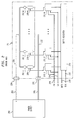
- FIG. 2 comprises the printhead 26, the power supply 201, a power supply bus 203, a power return bus 205, and power supply connection terminals 224 and 226.
- the printhead 26 comprises a power supply line 220, resistive heat elements 207-1, 207-2, . . . , 207-N, switches 209-1, 209-2, . . . , 209-N, a power return line 222, latches 211-1, 211-2, . . .
- Each of resistive heat elements 207-1 through 207-N has first and second electrodes.
- Each of switches 209-1 through 209-N has first, second and control terminals and each of latches 211-1 through 211-N has an input terminal, an output terminal, a latch terminal, and an enable terminal.
- the power supply 201 is coupled to a first end of the power supply bus 203 and to a first end of the power return bus 205.
- a second end of the power supply bus 203 is connected to the power supply line 220 in the printhead 26 through the power supply connection terminal 224 and a second end of the power return bus 205 is connected to the power return line 222 in the printhead 26 through the power supply connection terminal 226.
- the first electrode of each resistive heat element (e.g., 207-1 through 207-N) is connected to the power supply line 220.
- the second electrode of the resistive heat element 207-1 is connected to the first terminal of the switch 209-1.
- the second electrode of the resistive heat element 207-2 is connected to the first terminal of the switch 209-2 and the second electrode of the resistive heat element 207-N is connected to the first terminal of the switch 209-N.
- the second electrodes of the resistive heat elements 207-3 through 207-N-1 are similarly connected to the first terminals of switches 209-3 through 209-N-1 (not shown).
- the second terminal of each of switches 209-1 through 209-N is connected to the power return line 222.
- the control terminal of the switch 209-1 is coupled to the output terminal of the latch 211-1.
- the control terminal of the switch 209-2 is coupled to the output terminal of the latch 211-2 and the control terminal of the switch 209-N is coupled to the output terminal of the latch 211-N.
- the control terminals of switches 209-3 through 209-N-1 are similarly coupled to the output terminals of the latches 211-3 through 211-N-1 (not shown).
- the input terminals of latches 211-1 through 211 N are coupled to successive stages of the shift register 213.
- the latch terminals of latches 211-1 through 211-N are coupled to the latch line 229 and the enable terminals of latches 211-1 through 211-N are coupled to the enable line 228.
- a first input of the shift register 213 is coupled to the data line 230 and a second input of the shift register 213 is coupled to the clock line 232.
- the data codes are used to form a sequence of data bits which are transferred from the printhead control circuit 28 to the printhead 26 to energize the printhead heat elements 207-1 through 207-N.
- Each printhead heat element is energized by the number of data bits needed to produce the print density required at the corresponding pixel.
- the number of data bits may vary from zero to 255 for an 8 bit data code.
- the data bits DATA are serially shifted into the shift register 213 of FIG. 2 via the data line 230.
- a clock source (not shown) in the printhead control circuit 28 of a design well known in the art supplies signals CLK to the shift register 213 on the line 232 to control the shifting of the data bits into the shift register at a predetermined rate.
- the N data bits are received by the shift register 213, they are transferred to the latches 211-1 through 211-N by the latch pulse LA from line 229 in a manner well known in the art.
- Switches 209-1 through 209-N are closed responsive to the data bits in the corresponding latches and an enable pulse EN on the enable terminals of the latches 211-1 through 211-N so that the heat elements 207-1 through 207-N selectively receive current from the power line 220.
- the shift register 213 successively receives 256 sets of data bits which control the printhead heat elements 207-1 through 207-N so that the print density at each pixel of a print line corresponds to the data code stored in the printhead control circuit 28 for that pixel.
- the data bits in the latches 211-1 through 211-N and the enable pulses EN control the energy developed in the heat elements 207-1 through 207-N, respectively, and thereby determine the densities of the pixels of the print line.
- the latch 211-1 controls the switch 209-1 so that a number of predetermined width pulses corresponding to the data code in the printhead control circuit 28 are coupled to the control terminal of the switch 209-1.
- the switch 209-1 is closed in response to the enable pulse EN and the state of the latch 211-1.
- a predetermined width enable pulse EN closes the switch 209-1.
- the heat element 207-1 is energized by the power supply 201 in accordance with the density defined by the image pixel data code in the printhead control circuit 28.
- latches 211-2 through 211-N control the operations of switches 209-2 through 209-N to determine the heat generated by heat elements 207-2 through 207-N, respectively.
- pulse waveforms (volts) as a function of time (microseconds) illustrating the data bits supplied to the shift register 213, the clock signals used to insert the data bits into the shift register 213, the latch pulse used to insert the data bits into the latches 211-1 through 211-N, and the enable pulse used to transfer the data bits in the latches 211-1 through 211-N to control switches 209-1 through 209-N, respectively.
- the magnitudes of the waveforms are shown as uniform.
- a waveform 801 shows the clock pulses CLK on the line 232 which control the insertion of data bits into the shift register 213.
- a waveform 803 shows a portion of the data bit stream DATA on the line 230 corresponding to the data bits for one of the 256 sets of data bits transferred to the shift register 213 for a print line.
- a waveform 805 shows the latch pulse used to insert. the set of data bits shown in the waveform 803 into the latches 211-1 through 211-N.
- a waveform 807 shows an enable pulse EN that transfers the data bits in the latches 211-1 through 211-N to the control inputs of the switches 209-1 through 209-N.
- a latch pulse occurs at the end of the transfer of each set of data bits into the shift register 213.
- the data stream DATA on the line 230 shown in waveform 803 is shifted into the shift register 213 by clock signals CLK shown in waveform 801 so that each data bit is positioned to control a specified heat element.
- a data bit may be a zero (i.e., low level) bit or a one (i.e., high level) bit.
- the heat elements 207-1 through 207-N are energized by data bits that are ones. For example, the data bit labeled 1 of the waveform 803 (a one data bit) is positioned so that it is transferred to the latch 211-1 when the N data bit set for a print line are aligned in the shift register 213.
- the data bit labeled N (a one data bit) is positioned so that it is transferred to the latch 211-N.
- a one data bit is transferred from the shift register 213 into the latch 211-1 and the one data bit N is transferred into the latch 211-N.
- the enable pulse EN then provides a predetermined width pulse to the control input of each switch of switches 209-1 through 209-N for each latch that stores a one data bit.
- the data bits in the latches 211-1 and 211-N cause predetermined width pulses to be applied to the switches 209-1 and 209-N so that the heat energy in the corresponding heat elements 207-1 and 207-N are precisely controlled.
- each print line varies in accordance with the data supplied to the printhead 26.
- all, some, or none of the heat elements 207-1 through 207-N may be selected concurrently.
- Each selected resistive heat element is coupled to the power supply 201 through the power supply bus 203, the connection terminal 224, the power supply line 220, the power return line 222, the connection terminal 226, and the power return bus 205.
- the power supply 201 is well regulated.
- Voltage sense circuitry may be added as is well known in the art to compensate for the voltage drops in the power supply bus 203 and the power return bus 205. Consequently, the voltage between connection terminals 224 and 226 in FIG. 2 remains constant independent of the number of selected heat elements.
- connection terminals 224 and 226, the power supply line 220, the power return line 222 and intermediate wiring to the heat elements 207-1 through 207-N in the printhead cause the voltage between the first and second electrodes of the selected heat elements to vary as the current drawn by the printhead 26 changes.
- These resistances within the printhead form a "parasitic resistance” that reduces the energy supplied to the selected heat elements even though a well regulated power supply may be used.
- As more heat elements are selected for a print line more current is drawn by the printhead 26 and the voltage drop across the "parasitic resistance" increases. The voltage across each selected heat element is thereby reduced as the number of selected heat elements increases. Since the energy supplied to a selected heat element (e.g., 207-1) is proportional to the square of the voltage thereacross, the heat generated in the selected heat element changes as a function of the number of selected heat elements and the print density produced varies accordingly.
- line 901 is a plot of the voltage (volts) at the output of the power supply 201 in volts as a function of the printhead current in amperes and line 905 is a plot of the voltage across a selected resistive heat element (volts) as a function of the printhead current (amperes). Since the power supply 201 is well regulated, the line 901 is horizontal corresponding to a constant voltage over the full range of the printhead current. The line 905, however, slopes downward as the printhead current increases due to the voltage drop in the "parasitic resistance".
- a print line that results from a relatively small number of selected heat elements has densities corresponding to a higher heat element voltage than a print line resulting from a large number of selected heat elements.
- Such variations in print density are generally not noticeable in text type prints where only black and white pixels are used.
- image type prints however, a tone scale having a range of gradations is used. In such type prints, density variations greater than one percent may be discernible.
- FIG. 3 there is shown a block diagram of a voltage compensated thermal printhead power supply arrangement in accordance with the present invention.
- the voltage compensated thermal printhead power supply arrangement of FIG. 3 comprises the printhead 26, the power supply 201, and a voltage compensator 310.
- the printhead 26 and the power supply 201 are the same as shown in FIG. 2.
- the printhead 26 is connected as described with respect to FIG. 2.
- the power supply bus 203 in FIG. 3 is connected between a positive output of the power supply 201 and the connection terminal 224.
- the power return bus 205 in FIG. 3 is connected between a negative output of the power supply 201 and a first terminal of the voltage compensator 310.
- a second terminal of the voltage compensator 310 is coupled to the connection terminal 226 via the bus 320.
- data bits are shifted into the shift register 213 and transferred to the latches 211-1 through 211-N as previously described with respect to FIG. 2.
- the voltage compensator 310 is adapted to sense the number of selected heat elements in the printhead 26 and to modify the voltage applied between connection terminals 224 and 226 of the printhead so that the energy supplied to each printhead heat element is maintained at a constant level substantially independent of the number of selected heat elements. In this way, the aforementioned "parasitic resistance" voltage drop is offset to prevent variations of print density.
- FIG. 8 there is shown a graph that illustrates the voltage between the connection terminals 224 and 226 of FIG. 3 and the voltage across the selected heat elements in the printhead 26 of FIG. 3 as a function of the current drawn by the printhead.
- a line 1001 is a plot of the voltage across connection terminals 224 and 226 of FIG. 3 in volts as a function of the printhead current in amperes in the power supply bus 203
- a line 1005 is a plot of the voltage (volts) across a selected resistive heat element as a function of the printhead current (amperes) in the power supply bus 203 of FIG. 3.
- the power supply 201 in FIG. 3 may be well regulated voltage source that provides a substantially constant voltage equal to that required by the selected heat elements for normal density printing.
- the printhead current is relatively low (I1 in FIG. 8) and the voltage across the connection terminals 224 and 226 is substantially the same as the voltage across the selected heat element (V1 in FIG. 8).
- the voltage across the voltage compensator 310 decreases so that the voltage across connection terminals 224 and 226 (waveform 1001) is sufficient (Vn in FIG. 8) to maintain the voltage V1 across the selected heat elements.
- the printhead current increases to IN.
- the voltage across the voltage compensator 310 is adjusted to set the voltage between connection terminals 224 and 226 in FIG. 3 at VN so that the voltage V1 is maintained across the heat elements 207-1 through 207-N independent of the number of selected heat elements.
- the voltage compensator 310 is shown coupled to the power return bus 205. Alternatively, the voltage compensator 310 may be coupled to the power supply bus 203 without altering the operation of the compensation arrangement.
- FIG. 4 there is shown a schematic and block diagram of the voltage compensated thermal printhead power supply arrangement of FIG. 3 in accordance with the invention in which one type of voltage compensation circuit is illustrated.
- the voltage compensated thermal printhead power supply arrangement of FIG. 4 comprises the power supply 201, the power supply bus 203, the printhead 26, the voltage compensator 310 shown as a dashed line rectangle, the power return bus 205, the power return bus 320, and connection terminals 224 and 226.
- the printhead 26 in FIG. 4 is the same as that of FIG. 2 or FIG 3 but is shown schematically as two resistances 434 and 436 connected in series for purposes of illustration.
- the resistance 434 represents the combined resistances of the selected heat elements of the printhead 26 and the resistance 436 represents the "parasitic resistance” noted with respect to FIG. 3.
- the "parasitic resistance” includes the resistances of the connection terminals 224 and 226, the power supply line 220, the power return line 222 and intermediate wiring to the selected heat elements in the printhead.
- the power supply bus 203 in FIG. 4 is connected between the positive output of the power supply 201 and the connection terminal 224.
- the power return bus 205 is connected between the negative output of the power supply 201 and a terminal of the voltage compensator 310.
- the voltage compensator 310 is coupled to the connection terminal 226 via the return bus 320.
- Resistances 434 and 436 are connected in series between connection terminals 224 and 226.
- the voltage compensator 310 in FIG. 4 comprises an n-p-n transistor 413 having an emitter 415, a base 417 and a collector 419, a resistor 407, a bias network 423, a differential amplifier 409 and a non-inverting amplifier 411.
- the emitter 415 of the transistor 413 is coupled to the power supply bus 205.
- the base 417 of the transistor 413 is coupled to an output of the amplifier 411 and to a first terminal of the bias network 423.
- a second terminal. of the bias network 423 is connected to a reference potential Vref.
- the collector 419 of the transistor 413 is coupled to an inverting input of the differential amplifier 409 and to a first terminal of the resistor 407.
- a second terminal of the resistor 407 is coupled to a non-inverting input of the differential amplifier 409 and to the bus 320.
- An output of the amplifier 409 is coupled to an input of the non-inverting amplifier 411.
- the transistor 413 is biased close to saturation by the bias network 423 so that voltage between connection terminals 224 and 226 (i.e., the power supply output voltage Vo less the emitter-collector voltage Vt of transistor 413 less the voltage drop across the resistor 407) is equal to the prescribed heat element voltage Vh when one heat element is selected.
- the current through the resistor 407 increases and the voltage across the resistor 407 becomes larger. In this way, the number of selected heat elements is sensed.
- the value of the resistor 407 is generally very low (e.g., in the order of milliohms) and the voltage thereacross is relative small.
- the voltage across the resistor 407 is amplified in the differential amplifier 409 so that the voltage at the output thereof becomes more positive as the current across the resistor 407 increases.
- the output of the non-inverting amplifier 411 is coupled to the base 417 of the transistor 413 and is effective to drive the transistor 413 further toward saturation as the voltage across the resistor 407 increases.
- the emitter-collector voltage drop Vt of the transistor 413 decreases as the current through the resistor 407 becomes larger whereby the voltage across the printhead connection terminals 224 and 226 is increased. In this manner, the voltage across the connection terminals 224 and 226 of FIG.
- n-p-n transistor 413 in series with the power return bus 205 in FIG. 4 may be replaced by a transistor in series with the power supply bus 203.
- FIG. 5 there is shown a schematic and block diagram of the voltage compensation arrangement in accordance with the invention that is substantially the same as shown in FIG. 4 except that the adjustment of the voltage is performed in a voltage regulator that is coupled to the power supply.
- the voltage compensation arrangement of FIG. 5 comprises the power supply 201, the power supply bus 203, the printhead 26, the voltage compensator 310 shown within dashed lines, the power return bus 205, the power return bus 320, and connection terminals 224 and 226.
- the printhead 26 is represented as a resistance 534 connected in series with a resistance 536 and further comprises a temperature sensor 506.
- the voltage compensation arrangement of FIG. 5 is further modified to compensate for power bus voltage drops and temperature changes in the printhead.
- the printhead 26 and the power supply 201 are connected substantially as described with respect the printhead 26 in FIG. 4.
- the resistance 534 represents the combined resistances of the selected printhead heat elements and resistance 536 represents the "parasitic resistance” comprising the resistances of the connection terminals 224 and 226, power supply and return lines 220 and 222 and intermediate wiring in the printhead.
- the voltage compensator 310 in FIG. 5 comprises a resistor 507, differential amplifiers 509 and 511, resistors 502 and 504, and a voltage regulator 513.
- a first input of the voltage regulator 513 is coupled to the positive terminal of the power supply 201 and an output of the voltage regulator 513 is coupled to the power supply bus 203.
- the voltage regulator comprises a voltage sense arrangement (not shown) adapted to modify the output voltage of the power supply in response to the voltage applied to the sense input as is well known in the art.
- a first terminal of the resistor 507 is coupled to the power return bus 205 and to a first input of the amplifier 509.
- a second terminal of the resistor 507 is coupled to the connection terminal 226 via the return line 320 and to a second input of the amplifier 509.
- connection terminal 224 in FIG. 5 is coupled to a first terminal of the resistor 502, and a second terminal of resistor 502 is coupled to a first input of the differential amplifier 511 and to a first terminal of the resistor 504.
- a second terminal of the resistor 504 is coupled to a terminal 508 of the temperature sensing device 506 (e.g., a thermistor) in the printhead 26.
- a second terminal of the thermal sensing device 506 is connected to a reference potential Vrefl.
- An output of the differential amplifier 511 is coupled to a second input of the voltage regulator 513.
- a negative output of the power supply 201 is coupled to the power return bus 205.
- the current flowing through the resistance 534 passes through the resistor 507.
- the voltage drop across the resistor 507 is amplified by the differential amplifier 509 and coupled from the output of the amplifier 509 to an inverting input of the amplifier 511.
- the voltage at the output of the amplifier 509 is representative of the number of selected heat elements in the printhead 26.
- the voltage at the connection terminal 224 indicative of the voltage drop through the power supply bus 203 is coupled to a non-inverting input of the amplifier 511 through the resistor 502 and the voltage from the temperature sensing device 506 appearing at the terminal 508 is coupled to the non-inverting input of the amplifier 511 through the resistor 504.
- the signals from the output of the amplifier 509 and resistors 502 and 504 are combined and amplified in the amplifier 511.
- the resultant signal appearing at the output of the amplifier 511 is coupled to a sense input of the voltage regulator 513.
- the voltage across the voltage regulator 513 is adjusted to account for changes in print density due to the varying number of selected heat elements, the voltage drop between the power supply and the connection terminal 224 and the temperature of the printhead.
- the power supply voltage is modified in proportion to the voltage drop across the resistor 507.
- the voltage across the connection terminals 224 and 226 increases in proportion to the number of selected heat elements.
- any decrease in the voltage at the connection terminal 226 causes the power supply voltage to be increased and any increase in temperature detected by the temperature sensing device 506 causes the power supply voltage to decrease.
- the voltage across the connection terminals 224 and 226 in FIG. 3 provided by power supply 201 is modified by the operation of the voltage regulator 513 to maintain the selected heat element voltage at a value that is constant except for corrections due to temperature variations detected by the temperature sensitive device 506. While the voltage regulator 513 is shown as a separate circuit element of the voltage compensator 310 in FIG. 5 for purposes of illustration, it may be incorporated in the power supply 201 and serve the same function as is well known in the art.
- the present invention is particularly suitable for producing repeatable color thermal images of a high quality. Such color images can be made on prints, identification cards or the like.
Landscapes
- Electronic Switches (AREA)
Claims (10)
- Thermische Druckvorrichtung, die folgendes aufweist:
einen Druckkopf (26) mit ersten und zweiten Leistungsanschlüssen (224,226) und einer Vielzahl von Heizelementen (207-1,...), die parallel zwischen den ersten und zweiten Anschlüssen gekoppelt sind, und Leistungsversorgungsmittel, die mit den ersten und zweiten Anschlüssen des Druckkopfs gekoppelt sind, um Strom an die Heizelemente zu liefern, wobei die thermische Druckvorrichtung folgendes aufweist:
Steuermittel, die mit den Heizelementen gekoppelt sind zum Auswählen, welches der Heizelemente den durch die Leistungsversorgungsmittel gelieferten Strom erhält;
Leistungsabfühlmittel, die zwischen einem der Leistungsanschlüssen des Druckkopfs und den Leistungsversorgungsmitteln gekoppelt sind zum Abfühlen einer derzeitigen Leistungsanforderung des Druckkopfs wenn der Druckkopf in Betrieb ist; und
Spannungssteuermittel, die auf die abgefühlte derzeitige Leistungsanforderung des Druckkopfs ansprechen zum direkten Steuern der Spannung, die mit den ersten und zweiten Anschlüssen des Druckkopfs gekoppelt ist, um eine vorgeschriebene, im wesentlichen gleiche Spannung in jedem der ausgewählten Heizelemente beizubehalten. - Vorrichtung nach Anspruch 1, wobei die Leistungsabfühlmittel zum Abfühlen der derzeitigen Leistungsanforderung des Druckkopfs (26) Mittel aufweisen zum Erzeugen eines Signals, das dem Strom entspricht, der von den Leistungsversorgungsmitteln zu dem Druckkopf geliefert wird.
- Vorrichtung nach Anspruch 2, wobei die Mittel zum Steuern der Spannung, die mit den ersten und zweiten Anschlüssen des Druckkopfs gekoppelt sind, Mittel aufweisen, die auf das Signal, das den Strom anzeigt, der durch die Leistungsversorgungsmittel an die ausgewählten Heizelemente angelegt wird, ansprechen zum Modifizieren der Spannung, die mit den ersten und zweiten Anschlüssen des Druckkopfs gekoppelt ist, um die Spannung an jedem der ausgewählten Heizelemente auf einer vorgeschriebenen, im wesentlichen gleichen Spannung zu halten und zwar unabhängig von der Anzahl der ausgewählten Heizelemente.
- Vorrichtung nach Anspruch 3, wobei die Leistungsversorgungsmittel Mittel aufweisen zum Erzeugen einer ersten Spannung; und wobei die Mittel zum Modifizieren der Spannung die mit dem Druckkopf gekoppelt sind, Mittel aufweisen, die auf das Signal ansprechen, das den Strom anzeigt, der durch die Leistungsversorgungsmittel an den Druckkopf geliefert wird, zum Einstellen der Spannung, die mit den ersten und zweiten Anschlüssen gekoppelt ist, um die vorgeschriebene, im wesentlichen gleiche Spannung an jedem der ausgewählten Heizelemente in dem Druckkopf beizubehalten.
- Vorrichtung nach Anspruch 3, wobei die Mittel zum Modifizieren der Spannung, die mit dem Druckkopf gekoppelt ist, Spannungseinstellmittel aufweisen, die zwischen den Leistungsversorgungsmitteln und den ersten und zweiten Anschlüssen des Druckkopfs gekoppelt sind zum Einstellen der Spannung, die mit dem Druckkopf gekoppelt ist, um dieselbe vorgeschrieben, im wesentlichen gleiche Spannung an jedem der ausgewählten Heizelemente beizubehalten.
- Vorrichtung nach Anspruch 5, wobei die Spannungeinstellmittel eine Halbleitereinrichtung mit ersten, zweiten und Steuerelektroden aufweisen, wobei die ersten und zweiten Elektroden zwischen den Leistungsversorgungsmitteln und einem der ersten und zweiten Anschlüsse des Druckkopfs gekoppelt sind, und wobei die Steuerelektrode mit den Mitteln zum Erzeugen eines Signals, das die derzeitige Leistungsanforderung des Druckkopfs anzeigt, gekoppelt ist.
- Vorrichtung nach Anspruch 6, wobei die Leistungsabfühlmittel zum Erzeugen des Signals, das die derzeitige Leistungsanforderung des Druckkopfs anzeigt, folgendes aufweist:
Widerstandsmittel, die zwischen der zweiten Elektrode der Halbleitereinrichtung und dem Druckkopf gekoppelt sind; und
Verstärkermittel, die zwischen den Widerstandsmitteln und der Steuerelektrode der Halbleitereinrichtung gekoppelt sind. - Vorrichtung nach Anspruch 2, wobei die Vorrichtung ferner folgendes aufweist:
Mittel zum Erzeugen eines Signals, das die Temperatur des Druckkopfs anzeigt; und wobei die Spannungssteuermittel Mittel aufweisen, die zusammen auf das Signal ansprechen, das den Strom anzeigt, das von den Leistungsversorgungsmitteln zu dem Druckkopf geliefert wird und auf das Signal, das die Temperatur des Druckkopfs anzeigt zum Modifizieren der Spannung, die mit den ersten und zweiten Anschlüssen des Druckkopfs gekoppelt ist. - Vorrichtung nach Anspruch 1, wobei die Spannungseinstellmittel zwischen dem zweiten Leistungsanschluß des Druckkopfs und der Leistungsversorgung gekoppelt sind.
- Vorrichtung nach einem der Ansprüche 1-9, wobei die Leistungsabfühlmittel zwischen dem zweiten Leistungsanschluß des Druckkopfs und den Leistungsversorgungsmittel gekoppelt sind.
Applications Claiming Priority (3)
| Application Number | Priority Date | Filing Date | Title |
|---|---|---|---|
| US07/547,353 US5053790A (en) | 1990-07-02 | 1990-07-02 | Parasitic resistance compensation for thermal printers |
| US547353 | 1990-07-02 | ||
| PCT/US1991/004592 WO1992000195A1 (en) | 1990-07-02 | 1991-06-27 | Parasitic resistance compensation for thermal printers |
Publications (2)
| Publication Number | Publication Date |
|---|---|
| EP0489909A1 EP0489909A1 (de) | 1992-06-17 |
| EP0489909B1 true EP0489909B1 (de) | 1996-06-05 |
Family
ID=24184317
Family Applications (1)
| Application Number | Title | Priority Date | Filing Date |
|---|---|---|---|
| EP91914858A Expired - Lifetime EP0489909B1 (de) | 1990-07-02 | 1991-06-27 | Kompensation des parasitären widerstands für thermodrucker |
Country Status (5)
| Country | Link |
|---|---|
| US (1) | US5053790A (de) |
| EP (1) | EP0489909B1 (de) |
| JP (1) | JPH05502633A (de) |
| DE (1) | DE69120037T2 (de) |
| WO (1) | WO1992000195A1 (de) |
Families Citing this family (22)
| Publication number | Priority date | Publication date | Assignee | Title |
|---|---|---|---|---|
| US5144341A (en) * | 1991-04-26 | 1992-09-01 | Xerox Corporation | Thermal ink jet drivers device design/layout |
| FR2691926B1 (fr) * | 1992-06-03 | 1996-06-07 | Axiohm | Tete d'impression thermique avec regulation de l'apport d'energie aux points chauffants. |
| SG47435A1 (en) * | 1992-10-08 | 1998-04-17 | Hewlett Packard Co | Printhead with reduced interconnections to a printer |
| US5469203A (en) * | 1992-11-24 | 1995-11-21 | Eastman Kodak Company | Parasitic resistance compensation for a thermal print head |
| JP3060347B2 (ja) * | 1992-12-28 | 2000-07-10 | キヤノン株式会社 | 記録装置 |
| FR2708525B1 (fr) * | 1993-08-04 | 1995-10-20 | Sagem | Procédé de commande de la tête ligne d'un appareil d'impression thermique et appareil d'impression thermique pour la mise en Óoeuvre du procédé. |
| FR2708524B1 (fr) * | 1993-08-04 | 1995-09-29 | Sagem | Appareil d'impression thermique à tête ligne. |
| EP0648608A1 (de) * | 1993-10-14 | 1995-04-19 | Eastman Kodak Company | Kompensation des parasitären Widerstands für Thermodrucker |
| JPH07178948A (ja) * | 1993-12-24 | 1995-07-18 | Shinko Electric Co Ltd | サーマルプリンタ |
| US5745146A (en) * | 1994-02-15 | 1998-04-28 | Monarch Marking Systems, Inc. | Dynamic strobe compensation control for a barcode printer |
| AU680033B2 (en) * | 1994-10-05 | 1997-07-17 | Societe D'applications Generales D'electricite Et De Mecanique S A G E M | Thermal line-printer head |
| US5942094A (en) * | 1997-12-23 | 1999-08-24 | Elcorsy Technology Inc. | Printing head system for use in an electrocoagulation printing apparatus |
| US6729707B2 (en) * | 2002-04-30 | 2004-05-04 | Hewlett-Packard Development Company, L.P. | Self-calibration of power delivery control to firing resistors |
| US6755495B2 (en) * | 2001-03-15 | 2004-06-29 | Hewlett-Packard Development Company, L.P. | Integrated control of power delivery to firing resistors for printhead assembly |
| JP2001225457A (ja) * | 2000-02-15 | 2001-08-21 | Canon Inc | 記録装置および記録装置の電源制御方法 |
| JP3880411B2 (ja) * | 2001-01-31 | 2007-02-14 | キヤノン株式会社 | 記録装置 |
| TWI261415B (en) * | 2003-05-21 | 2006-09-01 | Leadtek Research Inc | Pulse interval to voltage converter and converting method thereof |
| US7719712B2 (en) * | 2003-09-24 | 2010-05-18 | Hewlett-Packard Development Company, L.P. | Variable drive for printhead |
| FR3038255B1 (fr) * | 2015-06-30 | 2017-07-28 | Ingenico Group | Procede de gestion d'une imprimante thermique, dispositif et programme correspondant |
| WO2019172873A1 (en) * | 2018-03-05 | 2019-09-12 | Hewlett-Packard Development Company, L.P. | Actuator fault indication via wires along busses |
| WO2019172872A1 (en) * | 2018-03-05 | 2019-09-12 | Hewlett-Packard Development Company, L.P. | Zonal actuator fault detection |
| US11318737B2 (en) | 2018-07-02 | 2022-05-03 | Hewlett-Packard Development Company, L.P. | Fluidic die with fire signal adjustment |
Family Cites Families (20)
| Publication number | Priority date | Publication date | Assignee | Title |
|---|---|---|---|---|
| JPS55124674A (en) * | 1979-03-22 | 1980-09-25 | Fuji Xerox Co Ltd | Driver for thermosensitive recording head |
| US4736089A (en) * | 1980-05-05 | 1988-04-05 | Texas Instruments Incorporated | Switching regulator for terminal printhead |
| JPS5763280A (en) * | 1980-10-03 | 1982-04-16 | Ricoh Co Ltd | Driving circuit for heat-sensitive recorder |
| JPS5814787A (ja) * | 1981-07-20 | 1983-01-27 | Sanyo Electric Co Ltd | フアクシミリ装置の感熱記録方式 |
| JPS58197063A (ja) * | 1982-05-13 | 1983-11-16 | Toshiba Corp | 印字ヘッド駆動方式 |
| US4434356A (en) * | 1982-12-22 | 1984-02-28 | International Business Machines Corporation | Regulated current source for thermal printhead |
| US4574293A (en) * | 1983-05-23 | 1986-03-04 | Fuji Xerox Co., Ltd. | Compensation for heat accumulation in a thermal head |
| JPS60143979A (ja) * | 1983-12-29 | 1985-07-30 | Nec Corp | サ−マルプリンタにおけるサ−マルヘツドの駆動方法 |
| JPS60147357A (ja) * | 1984-01-12 | 1985-08-03 | Fuji Xerox Co Ltd | サ−マルヘツド発熱体の抵抗値検出方法 |
| US4531134A (en) * | 1984-03-26 | 1985-07-23 | International Business Machines Corporation | Regulated voltage and approximate constant power for thermal printhead |
| JPS60253562A (ja) * | 1984-05-30 | 1985-12-14 | Hitachi Ltd | 熱記録ヘツド |
| JPS61230962A (ja) * | 1985-04-08 | 1986-10-15 | Sato :Kk | サ−マルヘツドの温度制御装置 |
| JPS61237570A (ja) * | 1985-04-12 | 1986-10-22 | Victor Co Of Japan Ltd | 熱転写形階調記録装置 |
| JPS6266953A (ja) * | 1985-09-19 | 1987-03-26 | Tokyo Electric Co Ltd | サ−マルヘツドの電源回路 |
| US4814787A (en) * | 1986-01-17 | 1989-03-21 | Fuji Photo Film Co., Ltd. | Method for compensating temperature to a thermal head |
| JPS62256576A (ja) * | 1986-04-30 | 1987-11-09 | Fuji Xerox Co Ltd | 感熱記録装置 |
| JPS62267164A (ja) * | 1986-05-16 | 1987-11-19 | Hitachi Ltd | ビデオプリンタ |
| US4816843A (en) * | 1986-06-04 | 1989-03-28 | Ricoh Company, Ltd. | Method of controlling a thermal head |
| US4827281A (en) * | 1988-06-16 | 1989-05-02 | Eastman Kodak Company | Process for correcting down-the-page nonuniformity in thermal printing |
| US4827279A (en) * | 1988-06-16 | 1989-05-02 | Eastman Kodak Company | Process for correcting across-the-head nonuniformity in thermal printers |
-
1990
- 1990-07-02 US US07/547,353 patent/US5053790A/en not_active Expired - Lifetime
-
1991
- 1991-06-27 JP JP3513623A patent/JPH05502633A/ja active Pending
- 1991-06-27 WO PCT/US1991/004592 patent/WO1992000195A1/en active IP Right Grant
- 1991-06-27 DE DE69120037T patent/DE69120037T2/de not_active Expired - Fee Related
- 1991-06-27 EP EP91914858A patent/EP0489909B1/de not_active Expired - Lifetime
Also Published As
| Publication number | Publication date |
|---|---|
| DE69120037D1 (de) | 1996-07-11 |
| US5053790A (en) | 1991-10-01 |
| EP0489909A1 (de) | 1992-06-17 |
| JPH05502633A (ja) | 1993-05-13 |
| DE69120037T2 (de) | 1997-02-06 |
| WO1992000195A1 (en) | 1992-01-09 |
Similar Documents
| Publication | Publication Date | Title |
|---|---|---|
| EP0489909B1 (de) | Kompensation des parasitären widerstands für thermodrucker | |
| CA1261201A (en) | Closed loop thermal printer for maintaining constant printing energy | |
| US4806950A (en) | Image recording apparatus for heat generation type | |
| EP0562626A1 (de) | Thermodruckkopf dessen Heizelemente mit Stromsensoren ausgerüstet sind | |
| JP2607514B2 (ja) | サーマル・プリント装置 | |
| KR950026684A (ko) | 프린팅 헤드, 이를 사용한 프린팅 방법 및 장치, 및 그 프린팅 헤드를 보정하는 장치 및 방법 | |
| US5163760A (en) | Method and apparatus for driving a thermal head to reduce parasitic resistance effects | |
| US5075698A (en) | Method of driving a recording head and a recording apparatus utilizing this method | |
| US5608442A (en) | Heating control for thermal printers | |
| US5786837A (en) | Method and apparatus for thermal printing with voltage-drop compensation | |
| US4652892A (en) | Gradation control device for thermal ink-transfer type printing apparatus | |
| JPH0630887B2 (ja) | サーマルプリンタ | |
| GB2147763A (en) | Printing apparatus | |
| US5287122A (en) | System and method of selecting the reproducible colors in a discrete reproduction system | |
| EP0260992A2 (de) | Gradationssteuervorrichtung für Druckgeräte vom Typ thermische Tintenübertragung | |
| EP0601658B1 (de) | Kalibrierungsverfahren für Heizelemente eines thermischen Kopfes in einem Thermodrucksystem | |
| US4642657A (en) | Recorder | |
| EP0648608A1 (de) | Kompensation des parasitären Widerstands für Thermodrucker | |
| JPS61224773A (ja) | 感熱転写階調制御装置 | |
| EP0437023B1 (de) | Belichtungssteuerung von Energiequellen | |
| EP0627319A1 (de) | Verfahren zum Korrigieren der Ungleichmässigkeit in einem Thermodrucksystem | |
| JPH07137328A (ja) | 中間調記録装置 | |
| JPS616981A (ja) | 感熱記録装置 | |
| JPH02153754A (ja) | 記録ヘツド及び前記記録ヘツドを用いた熱記録装置 | |
| US6616356B2 (en) | Method for controlling a thermal head to permit multicolor printing |
Legal Events
| Date | Code | Title | Description |
|---|---|---|---|
| PUAI | Public reference made under article 153(3) epc to a published international application that has entered the european phase |
Free format text: ORIGINAL CODE: 0009012 |
|
| AK | Designated contracting states |
Kind code of ref document: A1 Designated state(s): DE FR GB |
|
| 17P | Request for examination filed |
Effective date: 19920707 |
|
| 17Q | First examination report despatched |
Effective date: 19931221 |
|
| GRAH | Despatch of communication of intention to grant a patent |
Free format text: ORIGINAL CODE: EPIDOS IGRA |
|
| GRAA | (expected) grant |
Free format text: ORIGINAL CODE: 0009210 |
|
| AK | Designated contracting states |
Kind code of ref document: B1 Designated state(s): DE FR GB |
|
| REF | Corresponds to: |
Ref document number: 69120037 Country of ref document: DE Date of ref document: 19960711 |
|
| ET | Fr: translation filed | ||
| PLBE | No opposition filed within time limit |
Free format text: ORIGINAL CODE: 0009261 |
|
| STAA | Information on the status of an ep patent application or granted ep patent |
Free format text: STATUS: NO OPPOSITION FILED WITHIN TIME LIMIT |
|
| 26N | No opposition filed | ||
| REG | Reference to a national code |
Ref country code: GB Ref legal event code: IF02 |
|
| PGFP | Annual fee paid to national office [announced via postgrant information from national office to epo] |
Ref country code: DE Payment date: 20070629 Year of fee payment: 17 |
|
| PGFP | Annual fee paid to national office [announced via postgrant information from national office to epo] |
Ref country code: GB Payment date: 20070511 Year of fee payment: 17 |
|
| PGFP | Annual fee paid to national office [announced via postgrant information from national office to epo] |
Ref country code: FR Payment date: 20070605 Year of fee payment: 17 |
|
| GBPC | Gb: european patent ceased through non-payment of renewal fee |
Effective date: 20080627 |
|
| REG | Reference to a national code |
Ref country code: FR Ref legal event code: ST Effective date: 20090228 |
|
| PG25 | Lapsed in a contracting state [announced via postgrant information from national office to epo] |
Ref country code: DE Free format text: LAPSE BECAUSE OF NON-PAYMENT OF DUE FEES Effective date: 20090101 |
|
| PG25 | Lapsed in a contracting state [announced via postgrant information from national office to epo] |
Ref country code: GB Free format text: LAPSE BECAUSE OF NON-PAYMENT OF DUE FEES Effective date: 20080627 |
|
| PG25 | Lapsed in a contracting state [announced via postgrant information from national office to epo] |
Ref country code: FR Free format text: LAPSE BECAUSE OF NON-PAYMENT OF DUE FEES Effective date: 20080630 |