EP0488148A2 - Verfahren zur Herstellung eines MOS-Feldeffekttransistors - Google Patents
Verfahren zur Herstellung eines MOS-Feldeffekttransistors Download PDFInfo
- Publication number
- EP0488148A2 EP0488148A2 EP91120153A EP91120153A EP0488148A2 EP 0488148 A2 EP0488148 A2 EP 0488148A2 EP 91120153 A EP91120153 A EP 91120153A EP 91120153 A EP91120153 A EP 91120153A EP 0488148 A2 EP0488148 A2 EP 0488148A2
- Authority
- EP
- European Patent Office
- Prior art keywords
- etching
- substrate
- oxide film
- cleansing
- dry
- Prior art date
- Legal status (The legal status is an assumption and is not a legal conclusion. Google has not performed a legal analysis and makes no representation as to the accuracy of the status listed.)
- Withdrawn
Links
Images
Classifications
-
- H10P95/00—
-
- H10P70/18—
-
- H10D64/01336—
-
- H10P70/10—
-
- H10P70/12—
-
- H10D64/01346—
-
- Y—GENERAL TAGGING OF NEW TECHNOLOGICAL DEVELOPMENTS; GENERAL TAGGING OF CROSS-SECTIONAL TECHNOLOGIES SPANNING OVER SEVERAL SECTIONS OF THE IPC; TECHNICAL SUBJECTS COVERED BY FORMER USPC CROSS-REFERENCE ART COLLECTIONS [XRACs] AND DIGESTS
- Y10—TECHNICAL SUBJECTS COVERED BY FORMER USPC
- Y10S—TECHNICAL SUBJECTS COVERED BY FORMER USPC CROSS-REFERENCE ART COLLECTIONS [XRACs] AND DIGESTS
- Y10S148/00—Metal treatment
- Y10S148/017—Clean surfaces
-
- Y—GENERAL TAGGING OF NEW TECHNOLOGICAL DEVELOPMENTS; GENERAL TAGGING OF CROSS-SECTIONAL TECHNOLOGIES SPANNING OVER SEVERAL SECTIONS OF THE IPC; TECHNICAL SUBJECTS COVERED BY FORMER USPC CROSS-REFERENCE ART COLLECTIONS [XRACs] AND DIGESTS
- Y10—TECHNICAL SUBJECTS COVERED BY FORMER USPC
- Y10S—TECHNICAL SUBJECTS COVERED BY FORMER USPC CROSS-REFERENCE ART COLLECTIONS [XRACs] AND DIGESTS
- Y10S148/00—Metal treatment
- Y10S148/053—Field effect transistors fets
-
- Y—GENERAL TAGGING OF NEW TECHNOLOGICAL DEVELOPMENTS; GENERAL TAGGING OF CROSS-SECTIONAL TECHNOLOGIES SPANNING OVER SEVERAL SECTIONS OF THE IPC; TECHNICAL SUBJECTS COVERED BY FORMER USPC CROSS-REFERENCE ART COLLECTIONS [XRACs] AND DIGESTS
- Y10—TECHNICAL SUBJECTS COVERED BY FORMER USPC
- Y10S—TECHNICAL SUBJECTS COVERED BY FORMER USPC CROSS-REFERENCE ART COLLECTIONS [XRACs] AND DIGESTS
- Y10S438/00—Semiconductor device manufacturing: process
- Y10S438/906—Cleaning of wafer as interim step
-
- Y—GENERAL TAGGING OF NEW TECHNOLOGICAL DEVELOPMENTS; GENERAL TAGGING OF CROSS-SECTIONAL TECHNOLOGIES SPANNING OVER SEVERAL SECTIONS OF THE IPC; TECHNICAL SUBJECTS COVERED BY FORMER USPC CROSS-REFERENCE ART COLLECTIONS [XRACs] AND DIGESTS
- Y10—TECHNICAL SUBJECTS COVERED BY FORMER USPC
- Y10S—TECHNICAL SUBJECTS COVERED BY FORMER USPC CROSS-REFERENCE ART COLLECTIONS [XRACs] AND DIGESTS
- Y10S438/00—Semiconductor device manufacturing: process
- Y10S438/909—Controlled atmosphere
-
- Y—GENERAL TAGGING OF NEW TECHNOLOGICAL DEVELOPMENTS; GENERAL TAGGING OF CROSS-SECTIONAL TECHNOLOGIES SPANNING OVER SEVERAL SECTIONS OF THE IPC; TECHNICAL SUBJECTS COVERED BY FORMER USPC CROSS-REFERENCE ART COLLECTIONS [XRACs] AND DIGESTS
- Y10—TECHNICAL SUBJECTS COVERED BY FORMER USPC
- Y10S—TECHNICAL SUBJECTS COVERED BY FORMER USPC CROSS-REFERENCE ART COLLECTIONS [XRACs] AND DIGESTS
- Y10S438/00—Semiconductor device manufacturing: process
- Y10S438/974—Substrate surface preparation
Definitions
- This invention relates to a method of manufacturing a semiconductor device including a very reliable MOS-type field effect transistor (hereinafter called "MOSFET”) by removing metal impurities during cleansing of the surface of a substrate.
- MOSFET MOS-type field effect transistor
- the conventional cleansing process to be performed before forming a gate oxide film is exemplified by the following:
- a gate oxide film is formed by thermal oxidation.
- metal impurities in the oxide film on the substrate surface can be removed by eliminating the oxide film by an HF cleaning solution, while many impurity particles would be stuck on the surface of the substrate only by this cleansing process. Further, metal impurities existing chiefly in the cleaning solution would remain in the chemical oxide film formed by the RCA cleaning, and these impurities would be scattered in the gate oxide film, thus contaminating the gate oxide film. These impurities existing in the gate oxide film would affect on the pressure-resisting characteristic of the gate film and the TDDB (Time Dependent Dielectric Breakdown) characteristic, which is to be used in evaluating the reliability of the gate film, thus deteriorating the reliability of MOSFET.
- TDDB Time Dependent Dielectric Breakdown
- a method of manufacturing a semiconductor device including a MOS-type field effect transistor comprising the steps of: cleansing a surface of a substrate; forming, next to said cleansing, a gate oxide film on the cleansed surface of the substrate; dry-etching, during said cleansing step, the surface of the substrate in an ambient in which hydrogen fluoride and a substance containing at least a chloride atom coexist in gaseous state; and removing, during said cleansing step, an oxide film and metal impurities on the surface of the substrate.
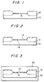
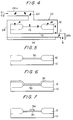
- FIGS. 1 through 7 show a series of manufacturing steps according to the first embodiment of this invention.
- an n-channel MOSFET is manufactured by the way of illustrative example.
- a source diffused region and a drain diffused region are formed by doping an n-type impurity such as arsenic in the usual method, and metallization is performed to form an electrode.
- the substance containing a chlorine atom was a chlorine gas for the most suitable example.
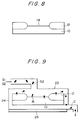
- FIGS. 8 and 9 shows a series of manufacturing steps according to the second embodiment of this invention.
- the silicon substrate 10 with a field oxide film 12 formed thereon (corresponding to the step (a)) is dry-cleaned directly by etching by a dry etching unit 22, omitting the RCA-cleaning step (step (b)) and the wet etching step (step (c)). Since the dry etching step shown in FIG. 9 is basically identical with the dry etching stop (the above-mentioned step (d)), its detailed description is omitted here for clarity.
- step (c) may be omitted in the first embodiment.
- a conventional alternative mean may be added at a necessary stage.
- this invention is also applicable to the production of an p-type MOSFET as well as a n-type MOSFET.
Landscapes
- Engineering & Computer Science (AREA)
- Manufacturing & Machinery (AREA)
- Power Engineering (AREA)
- Microelectronics & Electronic Packaging (AREA)
- Physics & Mathematics (AREA)
- Computer Hardware Design (AREA)
- Condensed Matter Physics & Semiconductors (AREA)
- General Physics & Mathematics (AREA)
- Chemical Kinetics & Catalysis (AREA)
- Crystallography & Structural Chemistry (AREA)
- General Chemical & Material Sciences (AREA)
- Chemical & Material Sciences (AREA)
- Insulated Gate Type Field-Effect Transistor (AREA)
- Cleaning Or Drying Semiconductors (AREA)
- Drying Of Semiconductors (AREA)
- Weting (AREA)
Applications Claiming Priority (2)
| Application Number | Priority Date | Filing Date | Title |
|---|---|---|---|
| JP321750/90 | 1990-11-26 | ||
| JP32175090 | 1990-11-26 |
Publications (2)
| Publication Number | Publication Date |
|---|---|
| EP0488148A2 true EP0488148A2 (de) | 1992-06-03 |
| EP0488148A3 EP0488148A3 (en) | 1992-08-12 |
Family
ID=18136031
Family Applications (1)
| Application Number | Title | Priority Date | Filing Date |
|---|---|---|---|
| EP19910120153 Withdrawn EP0488148A3 (en) | 1990-11-26 | 1991-11-26 | Method of manufacturing a mos-type field-effect transistor |
Country Status (4)
| Country | Link |
|---|---|
| US (1) | US5238871A (de) |
| EP (1) | EP0488148A3 (de) |
| JP (1) | JPH0521459A (de) |
| KR (1) | KR920010774A (de) |
Cited By (3)
| Publication number | Priority date | Publication date | Assignee | Title |
|---|---|---|---|---|
| DE19510922A1 (de) * | 1994-03-25 | 1995-09-28 | Mitsubishi Electric Corp | Verfahren zur Herstellung eines Halbleiterbauelements, Verfahren zur Reinigung einer Kristalloberfläche eines Halbleiters sowie Halbleiterbauelement |
| EP0692819A3 (de) * | 1994-07-07 | 1997-07-02 | Toshiba Kk | Verfahren zur Herstellung einer halbleitenden Anordnung mit einer Voroxidationstufe |
| EP0964439A1 (de) * | 1998-06-09 | 1999-12-15 | Air Products And Chemicals, Inc. | Gasphasen-Entfernen von Si02/metallischen Verunreinigungen von einem Siliziumsubstrat |
Families Citing this family (8)
| Publication number | Priority date | Publication date | Assignee | Title |
|---|---|---|---|---|
| US5589422A (en) * | 1993-01-15 | 1996-12-31 | Intel Corporation | Controlled, gas phase process for removal of trace metal contamination and for removal of a semiconductor layer |
| US5966623A (en) * | 1995-10-25 | 1999-10-12 | Eastman Kodak Company | Metal impurity neutralization within semiconductors by fluorination |
| JP3676912B2 (ja) * | 1997-08-07 | 2005-07-27 | 株式会社ルネサステクノロジ | 半導体製造装置およびその異物除去方法 |
| US5980770A (en) * | 1998-04-16 | 1999-11-09 | Siemens Aktiengesellschaft | Removal of post-RIE polymer on Al/Cu metal line |
| US6715497B2 (en) | 2001-01-02 | 2004-04-06 | International Business Machines Corporation | Treatment to eliminate polysilicon defects induced by metallic contaminants |
| US20020176984A1 (en) * | 2001-03-26 | 2002-11-28 | Wilson Smart | Silicon penetration device with increased fracture toughness and method of fabrication |
| JP2005275231A (ja) * | 2004-03-26 | 2005-10-06 | Fuji Photo Film Co Ltd | 感光性平版印刷版 |
| US20070048991A1 (en) * | 2005-08-23 | 2007-03-01 | Taiwan Semiconductor Manufacturing Co., Ltd. | Copper interconnect structures and fabrication method thereof |
Family Cites Families (4)
| Publication number | Priority date | Publication date | Assignee | Title |
|---|---|---|---|---|
| US3426422A (en) * | 1965-10-23 | 1969-02-11 | Fairchild Camera Instr Co | Method of making stable semiconductor devices |
| US4264374A (en) * | 1978-09-25 | 1981-04-28 | International Business Machines Corporation | Cleaning process for p-type silicon surface |
| JPH01204427A (ja) * | 1988-02-10 | 1989-08-17 | Hitachi Ltd | 半導体装置 |
| US4923828A (en) * | 1989-07-07 | 1990-05-08 | Eastman Kodak Company | Gaseous cleaning method for silicon devices |
-
1991
- 1991-11-25 US US07/796,825 patent/US5238871A/en not_active Expired - Fee Related
- 1991-11-25 KR KR1019910021221A patent/KR920010774A/ko not_active Withdrawn
- 1991-11-25 JP JP3309205A patent/JPH0521459A/ja active Pending
- 1991-11-26 EP EP19910120153 patent/EP0488148A3/en not_active Withdrawn
Cited By (7)
| Publication number | Priority date | Publication date | Assignee | Title |
|---|---|---|---|---|
| DE19510922A1 (de) * | 1994-03-25 | 1995-09-28 | Mitsubishi Electric Corp | Verfahren zur Herstellung eines Halbleiterbauelements, Verfahren zur Reinigung einer Kristalloberfläche eines Halbleiters sowie Halbleiterbauelement |
| GB2288067A (en) * | 1994-03-25 | 1995-10-04 | Mitsubishi Electric Corp | Removing oxide films during semiconductor device fabrication |
| GB2288067B (en) * | 1994-03-25 | 1997-11-12 | Mitsubishi Electric Corp | Method of fabricating a semiconductor device,method of cleaning a crystalline surface of a semiconductor,and semiconductor device |
| US5948161A (en) * | 1994-03-25 | 1999-09-07 | Mitsubishi Denki Kabushiki Kaisha | Method of fabricating a semiconductor device and method of cleaning a crystalline semiconductor surface |
| EP0692819A3 (de) * | 1994-07-07 | 1997-07-02 | Toshiba Kk | Verfahren zur Herstellung einer halbleitenden Anordnung mit einer Voroxidationstufe |
| US5731247A (en) * | 1994-07-07 | 1998-03-24 | Kabushiki Kaisha Toshiba | Method for manufacturing a semiconductor device including pre-oxidation process |
| EP0964439A1 (de) * | 1998-06-09 | 1999-12-15 | Air Products And Chemicals, Inc. | Gasphasen-Entfernen von Si02/metallischen Verunreinigungen von einem Siliziumsubstrat |
Also Published As
| Publication number | Publication date |
|---|---|
| EP0488148A3 (en) | 1992-08-12 |
| JPH0521459A (ja) | 1993-01-29 |
| KR920010774A (ko) | 1992-06-27 |
| US5238871A (en) | 1993-08-24 |
Similar Documents
| Publication | Publication Date | Title |
|---|---|---|
| US4808259A (en) | Plasma etching process for MOS circuit pregate etching utiliizing a multi-step power reduction recipe | |
| KR100933247B1 (ko) | 기판 처리 장치, 기판 처리 방법, 및 반도체 장치의 제조방법 | |
| US5238871A (en) | Method of manufacturing a semiconductor device | |
| US6048782A (en) | Method for doped shallow junction formation using direct gas-phase doping | |
| US6184155B1 (en) | Method for forming a ultra-thin gate insulator layer | |
| US6235590B1 (en) | Fabrication of differential gate oxide thicknesses on a single integrated circuit chip | |
| US4097314A (en) | Method of making a sapphire gate transistor | |
| JP2002280459A (ja) | 集積回路の製造方法 | |
| US5928786A (en) | Monocrystalline silicon wafer and method of thermally oxidizing a surface thereof | |
| JPH05109760A (ja) | 半導体装置 | |
| TW442897B (en) | Process for modified oxidation of a semiconductor substrate using chlorine plasma | |
| JPH05144802A (ja) | 半導体製造装置のクリーニング方法 | |
| JPH09320982A (ja) | 半導体集積回路装置の製造方法およびその製造装置 | |
| JPH0684865A (ja) | 半導体装置の乾式清浄化方法 | |
| JP3716007B2 (ja) | 半導体装置の製造方法 | |
| JPH03173131A (ja) | 半導体装置の製造方法 | |
| JPH11135508A (ja) | 半導体装置の製造方法 | |
| JPH10223605A (ja) | エッチング方法 | |
| GB2172743A (en) | Forming gate sidewall oxide spacers | |
| JPH0645593A (ja) | トランジスタの製造方法 | |
| US7148132B2 (en) | Manufacturing method of semiconductor device | |
| JPH08107205A (ja) | 犠牲酸化膜の製造方法 | |
| JPH0513359A (ja) | 半導体装置の製造方法 | |
| JPH07183515A (ja) | 半導体装置の製造方法 | |
| TW302514B (en) | Eliminating method of thin-film interface delamination of IC |
Legal Events
| Date | Code | Title | Description |
|---|---|---|---|
| PUAI | Public reference made under article 153(3) epc to a published international application that has entered the european phase |
Free format text: ORIGINAL CODE: 0009012 |
|
| AK | Designated contracting states |
Kind code of ref document: A2 Designated state(s): DE FR GB NL |
|
| PUAL | Search report despatched |
Free format text: ORIGINAL CODE: 0009013 |
|
| AK | Designated contracting states |
Kind code of ref document: A3 Designated state(s): DE FR GB NL |
|
| 17P | Request for examination filed |
Effective date: 19930119 |
|
| 17Q | First examination report despatched |
Effective date: 19941014 |
|
| STAA | Information on the status of an ep patent application or granted ep patent |
Free format text: STATUS: THE APPLICATION IS DEEMED TO BE WITHDRAWN |
|
| 18D | Application deemed to be withdrawn |
Effective date: 19950425 |