EP0484944B1 - Vektorrechnergerät, welches schnell eine Berechnung auf zwei Eingangsvektoren ausführen kann - Google Patents
Vektorrechnergerät, welches schnell eine Berechnung auf zwei Eingangsvektoren ausführen kann Download PDFInfo
- Publication number
- EP0484944B1 EP0484944B1 EP91118995A EP91118995A EP0484944B1 EP 0484944 B1 EP0484944 B1 EP 0484944B1 EP 91118995 A EP91118995 A EP 91118995A EP 91118995 A EP91118995 A EP 91118995A EP 0484944 B1 EP0484944 B1 EP 0484944B1
- Authority
- EP
- European Patent Office
- Prior art keywords
- vector
- signal
- adder
- zeroth
- selecting
- Prior art date
- Legal status (The legal status is an assumption and is not a legal conclusion. Google has not performed a legal analysis and makes no representation as to the accuracy of the status listed.)
- Expired - Lifetime
Links
Images


Classifications
-
- G—PHYSICS
- G06—COMPUTING OR CALCULATING; COUNTING
- G06F—ELECTRIC DIGITAL DATA PROCESSING
- G06F17/00—Digital computing or data processing equipment or methods, specially adapted for specific functions
- G06F17/10—Complex mathematical operations
- G06F17/16—Matrix or vector computation, e.g. matrix-matrix or matrix-vector multiplication, matrix factorization
Definitions
- This invention relates to a vector calculation apparatus for carrying out vector calculation on a plurality of vectors. It is to be noted throughout the instant specification that each of the vectors is composed of a plurality of vector components or elements. These are in the form of electrical signals for electrical processing, although a specific description will not be made hereinafter.
- a recent requirement for an electronic digital computer is to process a vector calculation at a high speed.
- the vector calculation is, for example, vector addition of calculating a sum of a pair of vectors.
- addition of components of the respective vectors must be repeated a great number of times. This is because each of the vectors is usually composed of many components.
- One conventional vector calculation apparatus includes a two-input vector adder for carrying out addition of two adder input signals. Supplied with the vectors as the adder input signals, the two-input vector adder carries out the addition to produce an adder output signal representative of the sum of vectors.
- This vector calculation apparatus requires a relatively long time as will later be described in detail.
- a different conventional vector calculation apparatus includes a three-input vector adder and a selecting circuit.
- the three-input vector adder is for carrying out addition of three adder input signals to produce an adder output signal.
- the selecting circuit is for selecting, as a selected signal, a selected one of the adder output signal and a predetermined value, such as zero. Supplied with the vectors and the selected signal as the adder input signals, the three-input vector adder carries out the addition to produce the adder output signal.
- this other vector calculation apparatus has a disadvantage in that a very long time is necessary to calculate the sum in the case where the vectors are composed of an enormous number of components.
- EP-A-0 214 775 discloses a multi-precision fixed/floating-point processor with a three-port ALU, four storage registers, a constant store circuit, and an output data register. Each of the registers is provided with three output ports and corresponding pass gates for selectively transferring data from the registers to the three inputs of the ALU.
- the constant store is also coupled to one of the input ports of the ALU by means of a pass gate. Results of the ALU are provided to the data output register for further processing.
- the conventional vector calculation apparatus is for use in carrying out vector addition of two vectors.
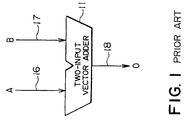
- the illustrated vector calculation apparatus comprises a two-input vector adder 11 which is connected to first and second input lines 16 and 17.
- the vectors are supplied as a first and a second adder input signal to the vector adder 11 through the first and the second input lines 16 and 17, respectively, and may be called first and second input vectors A and B (such vectors being denoted herein by capital letters rather than either by thick letters or by the capital letters with horizontal arrows over them).
- the first input vector A is composed of a sequence of first-set components or elements (a 1 , a 2 , ..., a n ) which may be called first through n-th components of the first input vector A, respectively.
- the second input vector B is composed of a sequence of second-set components (b 1 , b 2 , ..., b n ) which may be referred to as first through n-th components of the second input vector B. It is assumed in this manner in the illustrated example that the first input vector A has the same number of components as the second input vector B.
- the vector addition of the first and the second input vectors A and B is for calculating an output vector O composed of a sequence of output components (o 1 , o 2 , ..., o n ) which may be called first through n-th output components.
- the vector adder 11 successively sums up the first-set and the second-set components (a 1 , a 2 , ..., a n ) and (b 1 , b 2 , ..., b n ) to produce the first through the n-th output components (o 1 , o 2 , ..., o n ) which appear on an adder output line 18.
- Fig. 2 in addition to Fig. 1, the description will be made as regards calculation of a total sum of 2 k components of the first and the second input vectors A and B, where k represents a predetermined number, 2 k being not greater than n.
- a calculation time will be assumed to be equal to mT, where m is an integer and T is representative of a clock cycle which is determined by a sequence of clock pulses.
- the clock cycle is illustrated along a first or top row labelled CLK.
- the first-set components are depicted along a second row labelled A.
- the second-set components are illustrated along a third row labelled B.
- the adder output signal is shown along a fourth or bottom row labelled O.
- the 2 k components are divided at first into the first-set and the second-set components.
- the first-set components are 2 k-1 in number.
- the second-set components are also 2 k-1 in number.
- First ones a 1 and b 1 of the components of the first and the second input vectors A and B are supplied through the first and the second input lines 16 and 17 to the vector adder 11 in timed relation to a zeroth one of the clock pulses.
- second through 2 k-1 -th components of the first and the second input vectors A and B are successively supplied to the vector adder 11 in synchronism with first through (2 k-1 - 1)-th clock pulses, respectively.
- a simplified symbol r is substituted for 2 k-1 merely for simplification of illustration.
- a simplified symbol s is substituted for 2 k-2 merely for simplification of illustration.
- the simplified symbols will be used also in the following.
- the different conventional vector calculation apparatus comprises similar parts designated by like reference numerals.
- the vector calculation apparatus comprises a three-input vector adder 21 which is for carrying out vector addition of three vectors.
- the vector adder 21 is connected to a third input line 23 in addition to the first and the second input lines 16 and 17. Two of the vectors are supplied as the first and the second input vectors A and B to the vector adder 21 through the first and the second input lines 16 and 17.
- the remaining one of the three vectors is supplied as a third adder input signal to the vector adder 21 through the third input line 23 and may be called a third vector C (such a vector being also denoted herein by capital letters rather than by thick letters).
- the third vector C is composed of a sequence of third-set components and is assumed to have the same number of components as each of the first and the second vectors A and B.
- the vector adder 21 carries out the vector addition to produce an output vector D as an adder output signal representative of a result of the vector addition.
- the output vector D is composed of a sequence of output components (d 1 , d 2 , ..., d n ) which may be called first through n-th output components.
- the vector adder 21 successively sums up the first-set, the second-set, and the third-set components to produce the first through the n-th output components (d 1 , d 2 , ..., d n ) which appear on the output line 18.
- the vector calculation apparatus further comprises a selecting circuit 24 which is connected to the output and the third input lines 18 and 23 and to an additional input line 25.
- the selecting circuit 24 is for selecting, as a selected signal, one of the adder output signal and a predetermined value which may be "0" and is supplied through the additional input line 25.
- the selected signal is supplied as the third vector C to the vector adder 21 through the third input line 23. Therefore, the third vector C is composed of one of the predetermined value and the first through the n-th output components (d 1 , d 2 , ..., d n ).
- the first-set components are depicted along a first or top row labelled A.
- the second-set components are illustrated along a second row labelled B.
- the third-set components are illustrated along a third row labeled C.
- the adder output signal is shown along a fourth row labelled D.
- the operation of the vector calculation apparatus is controlled in accordance with each of successive timing cycles which comprises zeroth, first through (m - 1)-th, m-th, (m + 1)-th through (n - 1)-th, and n-th through (n + m - 1)-th cycle times 0, 1 to (m - 1), m, (m + 1) to (n - 1), n to (n + m - 1).
- the vector adder 21 produces first local addition results m times, when i varies from (2 k-1 - m + 1) to 2 k-1 through (2 k-1 - m + 2), ..., and so forth.
- the first local addition results are divided into a first and a second group.
- the operation of the vector calculation apparatus is carried out again with the first and the second groups supplied to the vector adder 21 as the first and the second input vectors A and B.
- the vector adder 21 produces second local addition results for use as the first and the second input vectors A and B. In this manner, the second local addition results are repeatedly obtained to result in the total sum of 2 k components.
- the calculation time of (2 k-1 + m - 1)T is required in order to obtain the first local addition results.
- the calculation time of ⁇ 2 p - 1 + p(m - 1) ⁇ T is required to obtain the second local addition results m times, where p represents a predetermined number, and m being as follows: 2 p > m > 2 p-1 .
- the vector calculation apparatus has a disadvantage in that a very long time is necessary to calculate the total calculation time in case where m is relatively great.
- the vector calculation apparatus comprises similar parts designated by like reference numerals.
- the selecting circuit 24 is referred to as a zeroth selecting arrangement.
- the vector calculation apparatus comprises first and second selecting circuits 26 and 27.
- the first selecting circuit 26 is connected to the first input line 16 and the three-input vector adder 21 and is for selecting, as a first selected signal, a selected one of the first-set components of a first vector supplied through input line 16 and the vector adder 21 output signal E.
- the second selecting circuit 27 is connected to the second input line 17, the vector adder 21, and a supplementary input line 28 and is for selecting, as a second selected signal, a selected one of the second-set components of a second vector supplied through input line 17, the vector adder 21 output signal E, and the predetermined value that is supplied through the supplementary input line 28.
- the vector calculation apparatus comprises zero selecting circuit 24 connected to the vector adder 21 and to a supplementary input line 25 and it is for selecting as zero-th selected signal a selected one of the vector adder 21 output signal E and the predetermined value that is supplied through the supplementary input line 25.
- the vector calculation apparatus further comprises a control circuit 29, a first register 31, a second register 32, and a third register 33.
- the control circuit 29 is connected to the vector adder 21 and the first through the third registers 31 to 33 and to the zeroth, the first, and the second selecting circuits 24, 26, and 27 through the first through the third registers 31 to 33 and is for controlling the vector adder 21, the first through the third registers 31 to 33 and the zeroth, the first, and the second selecting circuits 24, 27, and 28 as will later be described in detail.
- the first register 31 is connected to the vector adder 21 and the first selecting circuit 26 and is for memorizing the first selected signal as a first memorized signal to supply the first memorized signal as the first adder input signal to the vector adder 21 under control of the control circuit 29.
- the second register 32 is connected to the vector adder 21 and the second selecting circuit 27 and is for memorizing the second selected signal as a second memorized signal to supply the second memorized signal as the second adder input signal to the vector adder 21 under control of the control circuit 29.
- the third register 33 is connected to the vector adder 21 and the zeroth selecting circuit 24 and is for memorizing the zeroth selected signal as a zeroth memorized signal to supply the zeroth memorized signal as the third adder input signal to the vector adder 21 under control of the control circuit 29.
- a combination of the first through the third registers 31 to 33 is referred to as a supplying arrangement.
- the clock cycle is illustrated along a first or top row labelled CLK.
- the first-set components of the first vector are depicted along a second row labelled A.
- the second-set components of the second vector are illustrated along a third row labelled B.
- the first memorized signal is shown along a fourth row labelled 31.
- the second memorized signal is depicted along a fifth row labelled 32.
- the zeroth memorized signal is illustrated along a sixth row labelled 33.
- the adder output signal is shown along a seventh or bottom row labelled E.
- the operation of the vector calculation apparatus is controlled in accordance with each of successive timing cycles which comprise zeroth, first through ninth, tenth through seventeenth, eighteenth through twenty-sixth, twenty-seventh through n-th, (n + 1)-th, (n + 2)-th, (n + 3)-th through (n + 8)-th, (n + 9)-th through (n + 11)-th, (n + 12)-th through (n + 14)-th, (n + 15)-th through (n + 17)-th, and (n + 18)-th through (n + 26)-th cycle times 0, 1 to 9, 10 to 17, 18 to 26, 27 to 35, 36 to (n - 1), n, (n + 1), (n + 2), (n + 3) to (n + 8), (n + 9) to (n + 11), (n + 12) to (n + 14), (n + 15) to (n + 17), and (n + 18) to (n + 26).
- the first selecting circuit 26 selects the first-set components of the first vector (a 1 , a 2 , ..., a n ) as the first selected signal, one component in each of the timing cycles.
- the second selecting circuit 27 selects the second-set components of the second vector (b 1 , b 2 , ..., b n ) as the second selected signal.
- the control circuit 29 makes the zeroth selecting circuit 24 select the predetermined value as the zeroth selected signal although illustration is not made in Fig. 6.
- the first-set components of the first vector (a 1 , a 2 , ..., a n ) and the second-set components of the second vector (b 1 , b 2 , ..., b n ) are memorized as the first and the second memorized signals in the first and the second registers 31 and 32, respectively, during the first through the n-th cycle times 1 to n.
- the predetermined value is memorized as the zeroth memorized signal in the third register 33 at the first through the ninth cycle times 1 to 9.
- the first, the second, and the zeroth memorized signals are supplied as the first, the second, and the third adder input signals to the vector adder 21.
- the vector adder 21 carries out addition of the first, the second, and the third adder input signals at each of the first through the ninth cycle times 1 to 9 and produces first through ninth output components (e 1 , e 2 , ..., e 9 ) as the adder output signal at the ninth through the seventeenth cycle times 9 to 17.
- the zeroth selecting circuit 24 selects the adder output signal, namely, the first through the ninth output components (e 1 , e 2 , ..., e 9 ), one component in each of the timing cycles.
- the first through the ninth output components (e 1 , e 2 , ..., e 9 ) are memorized as the zeroth memorized signal in the third register 33.
- the first, the second, and the zeroth memorized signals are supplied as the first, the second, and the third adder input signals to the vector adder 21.
- the vector adder 21 carries out the addition of the first, the second, and the third adder input signals at each of the tenth through the eighteenth cycle times 10 to 18 and produces tenth through eighteenth output components (e 10 , e 11 , ..., e 18 ) as the adder output signal at the eighteenth through the twenty-sixth cycle times 18 to 26.
- the tenth through the eighteenth output components (e 10 , e 11 , ..., e 18 ) are memorized as the zeroth memorized signal in the third register 33.
- the vector adder 21 repeatedly carries out the addition to produce the first through the n-th output components (e 1 , e 2 , ..., e n ) as the adder output signal at the ninth through the (n + 8)-th cycle times 9 to n + 8.
- the control circuit 29 makes the zeroth selecting circuit 24 select the adder output signal as the selected signal to store the first through the n-th output components (e 1 , e 2 , ..., e n ) in the third register 33.
- the first selecting circuit 26 selects (n - 8)-th output component e n-8 to store the (n - 8)-th output component e n-8 in the first register 31.
- the second selecting circuit 27 selects the predetermined value to store the predetermined value in the second register 32.
- the zeroth selecting circuit 24 selects the predetermined value to store the predetermined value in the third register 33.
- the control circuit 29 controls the first register 31 to make the first register 31 hold the (n - 8)-th output component e n-8 .
- the second selecting circuit 27 selects (n - 7)-th output component e n-7 to store the (n - 7)-th output component e n-7 in the second register 32.
- the zeroth selecting circuit 24 selects the predetermined value to store the predetermined value in the third register 33.
- the control circuit 29 controls the first and the second registers 31 and 32 to hold the (n - 8)-th and the (n - 7)-th output components e n-8 and e n-7 in the first and the second registers 31 and 32.
- the zeroth selecting circuit 24 selects (n - 6)-th output component e n-6 to store the (n - 6)-th output component e n-6 in the third register 33.
- the (n - 8)-th, the (n - 7)-th, and the (n - 6)-th output components e n-8 , e n-7 , and e n-6 are supplied to the vector adder 21 and summed up in the vector adder 21 to produce (n + 3)-th output components e n+3 at the (n + 11)-th cycle time n + 11 under control of the control circuit 29.
- (n + 6)-th and (n + 9)-th output components e n+6 and e n+9 are produced from the vector adder 21 at the (n + 14)-th and (n + 17)-th cycle times n + 14 and n + 17 under control of the control circuit 29.
- the control circuit 29 makes the first, the second, and the zeroth selecting circuits 26, 27, and 24 select the adder output signal as each of the first, the second, and the zeroth selected signals in predetermined order.
- the first selecting circuit 26 selects the (n + 3)-th output component e n+3 to store the (n + 3)-th output component e n+3 in the first register 31.
- the second selecting circuit 27 selects the predetermined value to store the predetermined value in the second register 32.
- the zeroth selecting circuit 24 selects the predetermined value to store the predetermined value in the third register 33.
- the control circuit 29 controls the first register 31 to make the first register 31 hold the (n + 3)-th output component e n+3 .
- the control circuit 29 controls the second and the third registers 32 and 33 to make the second and the third registers 32 and 33 hold the predetermined value.
- the second selecting circuit 27 selects the (n + 6)-th output component e n+6 to store the (n + 6)-th output component e n+6 in the second register 32.
- the zeroth selecting circuit 24 selects again the predetermined value to store the predetermined value in the third register 33.
- the control circuit 29 controls the second register 32 to make the second register 32 hold the (n + 6)-th output component e n+6 .
- the zeroth selecting circuit 24 selects the (n + 9)-th output component e n+9 to store the (n + 9)-th output component e n+9 in the third register 33.
- the control circuit 29 controls the third register 33 to make the third register 33 hold the (n + 9)-th output component e n+9 .
- the (n + 3)-th, the (n + 6)-th, and the (n + 9)-th output components e n+3 , e n+6 , and e n+9 are supplied to the vector adder 21 and summed up in the vector adder 21 to produce (n + 18)-th output components e n+18 at the (n + 26)-th cycle time n + 26 under control of the control circuit 29.
- TCT (2 k-1 + 26)T.
- the vector calculation apparatus can carry out a vector calculation of two vectors at a high speed.
- control circuit 29 may be designed in such a manner that the vector adder 21 produces the adder output signal when less or more than eight cycle times lapse after the vector adder 21 is supplied with the first and the second adder input signals.
Landscapes
- Engineering & Computer Science (AREA)
- Physics & Mathematics (AREA)
- General Physics & Mathematics (AREA)
- Mathematical Physics (AREA)
- Pure & Applied Mathematics (AREA)
- Mathematical Analysis (AREA)
- Mathematical Optimization (AREA)
- Computational Mathematics (AREA)
- Data Mining & Analysis (AREA)
- Theoretical Computer Science (AREA)
- Computing Systems (AREA)
- Algebra (AREA)
- Databases & Information Systems (AREA)
- Software Systems (AREA)
- General Engineering & Computer Science (AREA)
- Complex Calculations (AREA)
Claims (3)
- Vorrichtung zur Berechnung eines Ergebnisses einer Vektorrechnung, die eine Addition eines ersten Vektors, der aus mehreren Komponenten einer ersten Menge besteht, und eines zweiten Vektors, der aus mehreren Komponenten einer zweiten Menge besteht, einschließt, wobei die Vorrichtung aufweist: einen Vektoraddierer (21), wobei der Vektoraddierer (21) drei Eingänge und einen Ausgang aufweist, zur Durchführung einer Addition eines ersten, eines zweiten und eines dritten Addierereingangssignals, das über die drei Eingänge an den Vektoraddierer (21) übergeben wird, um an dem Ausgang des Vektoraddierers (21) ein Addiererausgangssignal (E) als das Ergebnis zu erzeugen; eine Steuereinrichtung (29); eine nullte Wähleinrichtung (24), die mit dem Vektoraddierer (21) und der Steuereinrichtung (29) verbunden ist, zum Wählen, als nulltes gewähltes Signal, eines gewählten, nämlich entweder des Addiererausgangssignals (E) oder eines vorbestimmten Wertes, der über eine zusätzliche Eingangsleitung (25) übergeben wird;eine erste Wähleinrichtung (26), die mit dem Vektoraddierer (21) und der Steuereinrichtung (29) verbunden ist, zum Wählen, als erstes gewähltes Signal, einer bzw. eines gewählten, nämlich entweder der Komponenten der ersten Menge des ersten Vektors oder des Addiererausgangssignals (E);eine zweite Wähleinrichtung (27), die mit dem Vektoraddierer (21) und der Steuereinrichtung (29) verbunden ist, zum Wählen, als zweites gewähltes Signal, einer bzw. eines gewählten, nämlich entweder der Komponenten der zweiten Menge des zweiten Vektors oder des vorbestimmten Wertes, der über eine zusätzliche Eingangsleitung (28) übergeben wird, oder des Addiererausgangssignals (E);eine Registereinrichtung (31, 32, 33), die mit der ersten, zweiten und nullten Wähleinrichtung, der Steuereinrichtung (29) und dem Vektoraddierer (21) verbunden ist, zum temporären Speichern des ersten gewählten Signals, des zweiten gewählten Signals und des nullten gewählten Signals und zum Übergeben an den Vektoraddierer (21) des ersten gewählten Signals als das erste Addierereingangssignal, des zweiten gewählten Signals als das zweite Addierereingangssignal und des nullten gewählten Signals als das dritte Addierereingangssignal; und wobei das erste gewählte Signal, das zweite gewählte Signal und das nullte gewählte Signal vorher von der ersten (26), zweiten (27) und nullten (24) Wähleinrichtung entsprechend dem Betrieb der ersten, zweiten und nullten Wähleinrichtung gewählt worden sind, wie von der Steuereinrichtung (29) bestimmt; wobei die Steuereinrichtung (29) mit dem Vektoraddierer (21), der ersten, der zweiten und der nullten Wähleinrichtung und den Registereinrichtungen verbunden sind, zum Steuern des Vektoraddierers (21), der ersten, der zweiten und der nullten Wähleinrichtung (26, 27, 24) und der Registereinrichtungen (31, 32, 33); wobei die Registereinrichtungen (31, 32, 33) aufweisen:eine erste Registereinrichtung (31), die mit dem Vektoraddierer (21), der ersten Wähleinrichtung (26) und der Steuereinrichtung (29) verbunden ist, ferner mit einer Einrichtung zum temporären Speichern des ersten gewählten Signals als erstes gespeichertes Signal und einer Einrichtung, um das erste gespeicherte Signal als das erste Addierereingangssignal unter Steuerung der Steuereinrichtung (29) an den Vektoraddierer (21) zu übergeben;eine zweite Registereinrichtung (32), die mit dem Vektoraddierer (21), der zweiten Wähleinrichtung (27) und der Steuereinrichtung (29) verbunden ist, ferner mit einer Einrichtung zum temporären Speichern des zweiten gewählten Signals als zweites gespeichertes Signal und einer Einrichtung, um das zweite gespeicherte Signal als das zweite Addierereingangssignal unter Steuerung der Steuereinrichtung (29) an den Vektoraddierer (21) zu übergeben; undeine dritte Registereinrichtung (33), die mit dem Vektoraddierer (21), der nullten Wähleinrichtung (24) und der Steuereinrichtung (29) verbunden ist, ferner mit einer Einrichtung zum temporären Speichern des nullten gewählten Signals als nulltes gespeichertes Signal und einer Einrichtung, um das nullte gespeicherte Signal als das dritte Addierereingangssignal unter Steuerung der Steuereinrichtung (29) an den Vektoraddierer (21) zu übergeben;wobei die Steuereinrichtung (29) ferner eine Einrichtung aufweist, um die zweite Wähleinrichtung (27) und die nullte Wähleinrichtung (24) derartig zu steuern, daß gleichzeitig die zweite Wähleinrichtung (27) und die nullte Wähleinrichtung (24) den vorbestimmten Wert als das nullte gewählte Signal und als das zweite gewählte Signal wählen, die jeweils über die zusätzliche Eingangsleitung (25) und die zusätzliche Eingangsleitung (28) übergeben werden.
- Vorrichtung nach Anspruch 1, wobei die Steuereinrichtung aufweist:eine steuernde Einrichtung (29), die mit der ersten Wähleinrichtung (26), der zweiten Wähleinrichtung (27) und der nullten Wähleinrichtung (24) verbunden ist, um die erste Wähleinrichtung, die zweite Wähleinrichtung und die nullte Wähleinrichtung so zu steuern, daß die folgenden Auswahlen von Signalen an die erste (31), die zweite (32) und die dritte (33) Registereinrichtung übergeben werden, indem die erste, zweite und nullte Wähleinrichtung entsprechend betrieben wird:eine erste Auswahl, bei der eine gewählte der Komponenten der ersten Menge des ersten Vektors als erstes gewähltes Signal an die erste Registereinrichtung (31) übergeben wird, eine gewählte der Komponenten der zweiten Menge des zweiten Vektors als zweites gewähltes Signal an die zweite Registereinrichtung (32) übergeben wird, und der vorbestimmte Wert als nulltes gewähltes Signal an die dritte Registereinrichtung (33) übergeben wird;eine zweite Auswahl, bei der eine gewählte der Komponenten der ersten Menge des ersten Vektors als erstes gewähltes Signal an die erste Registereinrichtung (31) übergeben wird, eine gewählte der Komponenten der zweiten Menge des zweiten Vektors als zweites gewähltes Signal an die zweite Registereinrichtung (32) übergeben wird und das Ausgangssignal (E) des Vektoraddierers (21) als nulltes gewähltes Signal an die dritte Registereinrichtung (33) übergeben wird;eine dritte Auswahl, bei der das Ausgangssignal (E) des Vektoraddierers (21) als erstes gewähltes Signal an die erste Registereinrichtung (31) übergeben wird, der vorbestimmte Wert als zweites gewähltes Signal an die zweite Registereinrichtung (32) übergeben wird und der vorbestimmte Wert als nulltes gewähltes Signal an die dritte Registereinrichtung (33) übergeben wird;wobei die Steuereinrichtung (29) ferner eine Einrichtung aufweist, um entweder die erste Auswahl oder die zweite Auswahl oder die dritte Auswahl zu wählen und um die erste, zweite und nullte Wähleinrichtung in einer vorbestimmten Reihenfolge von Betriebsschritten entsprechend zu betreiben.
- Vorrichtung nach Anspruch 2, wobei die Steuereinrichtung aufweist:eine steuernde Einrichtung (29), die mit der ersten Wähleinrichtung (26), der zweiten Wähleinrichtung (27) und der nullten Wähleinrichtung (24) verbunden ist, um die erste Wähleinrichtung, die zweite Wähleinrichtung und die nullte Wähleinrichtung so zu steuern, daß die folgenden Auswahlen von Signalen an die erste (31), die zweite (32) und die dritte (33) Registereinrichtung übergeben werden, indem die erste, zweite und nullte Wähleinrichtung entsprechend betrieben werden:eine vierte Auswahl, bei der kein Signal als erstes gewähltes Signal an die erste Registereinrichtung (31) übergeben wird, das Ausgangssignal (E) des Vektoraddierers (21) als zweites gewähltes Signal an die zweite Registereinrichtung (32) übergeben wird und der vorbestimmte Wert als nulltes gewähltes Signal an die dritte Registereinrichtung (33) übergeben wird;eine fünfte Auswahl, bei der kein Signal als erstes gewähltes Signal an die erste Registereinrichtung (31) übergeben wird, kein Signal als zweites gewähltes Signal an die zweite Registereinrichtung (32) übergeben wird und ein Ausgangssignal (E) des Vektoraddierers (21) als nulltes gewähltes Signal an die Registereinrichtung (33) übergeben wird;wobei die Steuereinrichtung (29) ferner eine Einrichtung aufweist, um entweder die erste Auswahl oder die zweite Auswahl oder die dritte Auswahl oder die vierte Auswahl oder die fünfte Auswahl zu wählen und um die erste (26), die zweite (27) und die nullte (24) Wähleinrichtung entsprechend zu betreiben, in einer vorbestimmten Reihenfolge von Arbeitsschritten.
Applications Claiming Priority (3)
| Application Number | Priority Date | Filing Date | Title |
|---|---|---|---|
| JP303504/90 | 1990-11-08 | ||
| JP30350490 | 1990-11-08 | ||
| JP2303504A JPH04177462A (ja) | 1990-11-08 | 1990-11-08 | ベクトル総和演算装置 |
Publications (3)
| Publication Number | Publication Date |
|---|---|
| EP0484944A2 EP0484944A2 (de) | 1992-05-13 |
| EP0484944A3 EP0484944A3 (en) | 1993-05-05 |
| EP0484944B1 true EP0484944B1 (de) | 1999-09-15 |
Family
ID=17921771
Family Applications (1)
| Application Number | Title | Priority Date | Filing Date |
|---|---|---|---|
| EP91118995A Expired - Lifetime EP0484944B1 (de) | 1990-11-08 | 1991-11-07 | Vektorrechnergerät, welches schnell eine Berechnung auf zwei Eingangsvektoren ausführen kann |
Country Status (6)
| Country | Link |
|---|---|
| US (1) | US5493521A (de) |
| EP (1) | EP0484944B1 (de) |
| JP (1) | JPH04177462A (de) |
| AU (1) | AU650068B2 (de) |
| CA (1) | CA2055144C (de) |
| DE (1) | DE69131613T2 (de) |
Families Citing this family (7)
| Publication number | Priority date | Publication date | Assignee | Title |
|---|---|---|---|---|
| KR970002394B1 (ko) * | 1994-05-09 | 1997-03-05 | 삼성전자 주식회사 | 산술 논리 연산장치와 다중 가산기들 사이의 데이타 전송회로 |
| JPH08241301A (ja) * | 1995-03-07 | 1996-09-17 | Nec Corp | 直交変換処理装置 |
| US5984515A (en) * | 1995-12-15 | 1999-11-16 | Intel Corporation | Computer implemented method for providing a two dimensional rotation of packed data |
| AU1465497A (en) * | 1995-12-19 | 1997-07-28 | Intel Corporation | A computer system performing a two-dimensional rotation of packed data representing multimedia information |
| EP2116821B1 (de) | 2008-05-09 | 2013-07-17 | Rademaker B.V. | Vorrichtung und Verfahren zum Wiegen eines Produktflusses |
| US12592470B2 (en) | 2023-10-30 | 2026-03-31 | Tas Lobe Invest As | Analog vector summing device |
| NO20231156A1 (en) * | 2023-10-30 | 2025-05-01 | Tas Lobe Invest As | Analogue Vector Summing |
Family Cites Families (8)
| Publication number | Priority date | Publication date | Assignee | Title |
|---|---|---|---|---|
| US3331954A (en) * | 1964-08-28 | 1967-07-18 | Gen Precision Inc | Computer performing serial arithmetic operations having a parallel-type static memory |
| JPS55103642A (en) * | 1979-02-01 | 1980-08-08 | Tetsunori Nishimoto | Division unit |
| JPS60136875A (ja) * | 1983-12-26 | 1985-07-20 | Hitachi Ltd | ベクトル演算器 |
| US4748580A (en) * | 1985-08-30 | 1988-05-31 | Advanced Micro Devices, Inc. | Multi-precision fixed/floating-point processor |
| JPH0746351B2 (ja) * | 1987-03-04 | 1995-05-17 | 日本電気株式会社 | ベクトル演算装置 |
| EP0281132B1 (de) * | 1987-03-04 | 1995-10-25 | Nec Corporation | Vektorrechnerschaltung, welche schnell eine Berechnung auf drei Eingangsvektoren ausführen kann |
| EP0314809B1 (de) * | 1987-05-14 | 1993-07-21 | Fujitsu Limited | Vektorprozessor zur schnellen verarbeitung von rekursiven gleichungen |
| JP2512778B2 (ja) * | 1988-01-13 | 1996-07-03 | 株式会社日立製作所 | 演算処理方法 |
-
1990
- 1990-11-08 JP JP2303504A patent/JPH04177462A/ja active Pending
-
1991
- 1991-11-07 CA CA002055144A patent/CA2055144C/en not_active Expired - Fee Related
- 1991-11-07 EP EP91118995A patent/EP0484944B1/de not_active Expired - Lifetime
- 1991-11-07 DE DE69131613T patent/DE69131613T2/de not_active Expired - Fee Related
- 1991-11-08 AU AU87711/91A patent/AU650068B2/en not_active Ceased
-
1994
- 1994-03-09 US US08/208,081 patent/US5493521A/en not_active Expired - Fee Related
Also Published As
| Publication number | Publication date |
|---|---|
| EP0484944A3 (en) | 1993-05-05 |
| JPH04177462A (ja) | 1992-06-24 |
| CA2055144C (en) | 1997-08-19 |
| DE69131613D1 (de) | 1999-10-21 |
| EP0484944A2 (de) | 1992-05-13 |
| DE69131613T2 (de) | 2000-03-02 |
| AU650068B2 (en) | 1994-06-09 |
| AU8771191A (en) | 1992-05-14 |
| US5493521A (en) | 1996-02-20 |
| CA2055144A1 (en) | 1992-05-09 |
Similar Documents
| Publication | Publication Date | Title |
|---|---|---|
| US5381357A (en) | Complex adaptive fir filter | |
| US5301344A (en) | Multibus sequential processor to perform in parallel a plurality of reconfigurable logic operations on a plurality of data sets | |
| US4790026A (en) | Programmable pipelined image processor | |
| EP0976059B1 (de) | Feldprogrammierbarer prozessor | |
| KR880006617A (ko) | 직각 변환 처리기 | |
| EP0484944B1 (de) | Vektorrechnergerät, welches schnell eine Berechnung auf zwei Eingangsvektoren ausführen kann | |
| US5034910A (en) | Systolic fast Fourier transform method and apparatus | |
| US4852040A (en) | Vector calculation circuit capable of rapidly carrying out vector calculation of three input vectors | |
| EP0373468B1 (de) | Pipelineprozessor zur Durchführung des LMS Algorithmus | |
| JP2645213B2 (ja) | 離散余弦変換回路 | |
| US4328425A (en) | Filter for image pixels | |
| US3997771A (en) | Apparatus and method for performing an arithmetic operation and multibit shift | |
| US5029079A (en) | Apparatus and method for flexible control of digital signal processing devices | |
| JP3668356B2 (ja) | 高速フーリエ変換演算回路 | |
| US6240062B1 (en) | Fast fourier transform calculating apparatus and fast fourier transform calculating method | |
| US4490805A (en) | High speed multiply accumulate processor | |
| US5774388A (en) | Device for electronically calculating a fourier transform and method of minimizing the size of internal data paths within such a device | |
| US5331584A (en) | Discrete cosine transformation processor | |
| US4843584A (en) | Cordic implementation of multi-dimensional plane rotation over the complex field | |
| KR960019970A (ko) | 신호처리장치 | |
| US5309385A (en) | Vector division processing method and system | |
| EP0535395B1 (de) | Teilmultiplikatorselektor für Multiplikationsschaltung | |
| KR100193385B1 (ko) | 단일화된 시스톨릭어레이 구조에 의한 dct/dst/dht의 수행 방법 및 그 장치 | |
| JPS60220466A (ja) | 高速フ−リエ変換装置 | |
| SE428252B (sv) | Dataoverforingsanordning |
Legal Events
| Date | Code | Title | Description |
|---|---|---|---|
| PUAI | Public reference made under article 153(3) epc to a published international application that has entered the european phase |
Free format text: ORIGINAL CODE: 0009012 |
|
| 17P | Request for examination filed |
Effective date: 19911204 |
|
| AK | Designated contracting states |
Kind code of ref document: A2 Designated state(s): BE DE FR GB IT NL SE |
|
| PUAL | Search report despatched |
Free format text: ORIGINAL CODE: 0009013 |
|
| AK | Designated contracting states |
Kind code of ref document: A3 Designated state(s): BE DE FR GB IT NL SE |
|
| 17Q | First examination report despatched |
Effective date: 19960102 |
|
| GRAG | Despatch of communication of intention to grant |
Free format text: ORIGINAL CODE: EPIDOS AGRA |
|
| GRAG | Despatch of communication of intention to grant |
Free format text: ORIGINAL CODE: EPIDOS AGRA |
|
| GRAG | Despatch of communication of intention to grant |
Free format text: ORIGINAL CODE: EPIDOS AGRA |
|
| GRAH | Despatch of communication of intention to grant a patent |
Free format text: ORIGINAL CODE: EPIDOS IGRA |
|
| GRAH | Despatch of communication of intention to grant a patent |
Free format text: ORIGINAL CODE: EPIDOS IGRA |
|
| GRAA | (expected) grant |
Free format text: ORIGINAL CODE: 0009210 |
|
| AK | Designated contracting states |
Kind code of ref document: B1 Designated state(s): BE DE FR GB IT NL SE |
|
| REF | Corresponds to: |
Ref document number: 69131613 Country of ref document: DE Date of ref document: 19991021 |
|
| ITF | It: translation for a ep patent filed | ||
| ET | Fr: translation filed | ||
| PLBE | No opposition filed within time limit |
Free format text: ORIGINAL CODE: 0009261 |
|
| STAA | Information on the status of an ep patent application or granted ep patent |
Free format text: STATUS: NO OPPOSITION FILED WITHIN TIME LIMIT |
|
| 26N | No opposition filed | ||
| REG | Reference to a national code |
Ref country code: GB Ref legal event code: IF02 |
|
| PGFP | Annual fee paid to national office [announced via postgrant information from national office to epo] |
Ref country code: BE Payment date: 20021021 Year of fee payment: 12 |
|
| PGFP | Annual fee paid to national office [announced via postgrant information from national office to epo] |
Ref country code: GB Payment date: 20021106 Year of fee payment: 12 |
|
| PGFP | Annual fee paid to national office [announced via postgrant information from national office to epo] |
Ref country code: DE Payment date: 20021107 Year of fee payment: 12 |
|
| PGFP | Annual fee paid to national office [announced via postgrant information from national office to epo] |
Ref country code: FR Payment date: 20021108 Year of fee payment: 12 |
|
| PGFP | Annual fee paid to national office [announced via postgrant information from national office to epo] |
Ref country code: SE Payment date: 20021112 Year of fee payment: 12 |
|
| PGFP | Annual fee paid to national office [announced via postgrant information from national office to epo] |
Ref country code: NL Payment date: 20021129 Year of fee payment: 12 |
|
| PG25 | Lapsed in a contracting state [announced via postgrant information from national office to epo] |
Ref country code: GB Free format text: LAPSE BECAUSE OF NON-PAYMENT OF DUE FEES Effective date: 20031107 |
|
| PG25 | Lapsed in a contracting state [announced via postgrant information from national office to epo] |
Ref country code: SE Free format text: LAPSE BECAUSE OF NON-PAYMENT OF DUE FEES Effective date: 20031108 |
|
| PG25 | Lapsed in a contracting state [announced via postgrant information from national office to epo] |
Ref country code: BE Free format text: LAPSE BECAUSE OF NON-PAYMENT OF DUE FEES Effective date: 20031130 |
|
| BERE | Be: lapsed |
Owner name: *NEC CORP. Effective date: 20031130 |
|
| PG25 | Lapsed in a contracting state [announced via postgrant information from national office to epo] |
Ref country code: NL Free format text: LAPSE BECAUSE OF NON-PAYMENT OF DUE FEES Effective date: 20040601 |
|
| PG25 | Lapsed in a contracting state [announced via postgrant information from national office to epo] |
Ref country code: DE Free format text: LAPSE BECAUSE OF NON-PAYMENT OF DUE FEES Effective date: 20040602 |
|
| EUG | Se: european patent has lapsed | ||
| GBPC | Gb: european patent ceased through non-payment of renewal fee |
Effective date: 20031107 |
|
| PG25 | Lapsed in a contracting state [announced via postgrant information from national office to epo] |
Ref country code: FR Free format text: LAPSE BECAUSE OF NON-PAYMENT OF DUE FEES Effective date: 20040730 |
|
| NLV4 | Nl: lapsed or anulled due to non-payment of the annual fee |
Effective date: 20040601 |
|
| REG | Reference to a national code |
Ref country code: FR Ref legal event code: ST |
|
| PG25 | Lapsed in a contracting state [announced via postgrant information from national office to epo] |
Ref country code: IT Free format text: LAPSE BECAUSE OF NON-PAYMENT OF DUE FEES;WARNING: LAPSES OF ITALIAN PATENTS WITH EFFECTIVE DATE BEFORE 2007 MAY HAVE OCCURRED AT ANY TIME BEFORE 2007. THE CORRECT EFFECTIVE DATE MAY BE DIFFERENT FROM THE ONE RECORDED. Effective date: 20051107 |