EP0482642B1 - Zusammengesetzter magnetoresistiver Dünnfilmmagnetkopf - Google Patents
Zusammengesetzter magnetoresistiver Dünnfilmmagnetkopf Download PDFInfo
- Publication number
- EP0482642B1 EP0482642B1 EP19910118167 EP91118167A EP0482642B1 EP 0482642 B1 EP0482642 B1 EP 0482642B1 EP 19910118167 EP19910118167 EP 19910118167 EP 91118167 A EP91118167 A EP 91118167A EP 0482642 B1 EP0482642 B1 EP 0482642B1
- Authority
- EP
- European Patent Office
- Prior art keywords
- magnetic
- thin
- film
- magneto
- film magnetic
- Prior art date
- Legal status (The legal status is an assumption and is not a legal conclusion. Google has not performed a legal analysis and makes no representation as to the accuracy of the status listed.)
- Expired - Lifetime
Links
Images


Classifications
-
- G—PHYSICS
- G11—INFORMATION STORAGE
- G11B—INFORMATION STORAGE BASED ON RELATIVE MOVEMENT BETWEEN RECORD CARRIER AND TRANSDUCER
- G11B5/00—Recording by magnetisation or demagnetisation of a record carrier; Reproducing by magnetic means; Record carriers therefor
- G11B5/127—Structure or manufacture of heads, e.g. inductive
- G11B5/33—Structure or manufacture of flux-sensitive heads, i.e. for reproduction only; Combination of such heads with means for recording or erasing only
- G11B5/39—Structure or manufacture of flux-sensitive heads, i.e. for reproduction only; Combination of such heads with means for recording or erasing only using magneto-resistive devices or effects
- G11B5/3903—Structure or manufacture of flux-sensitive heads, i.e. for reproduction only; Combination of such heads with means for recording or erasing only using magneto-resistive devices or effects using magnetic thin film layers or their effects, the films being part of integrated structures
- G11B5/3967—Composite structural arrangements of transducers, e.g. inductive write and magnetoresistive read
Definitions
- the present invention relates to a composite type thin film magnetic head formed by integrating a reproducing magnetic head of a magneto-resistance effect type and a recording magnetic head of an inductive type, which composite type thin film magnetic head is suitably used as a recording and reproducing magnetic head for a hard disk drive, for example.
- a composite type thin-film magnetic head tends to be used.
- the composite type thin-film magnetic head is formed by integrating a magneto-resistance effect type magnetic head (which will be hereinafter referred to as an MR magnetic head) having a superior sensitivity to a short wavelength which magnetic head is used in reproduction and an inductive type magnetic head which is used in recording.
- an MR magnetic head magneto-resistance effect type magnetic head
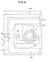
- Figs. 5 and 6 are schematic sectional and plan views of such a composite type thin-film magnetic head, respectively.
- reference numeral 1 denotes a substrate constructed of a slider (not shown) adapted to fly from a magnetic recording medium (not shown), e.g., a hard disk for use with a hard disk drive, due to an air flow caused by rotation of the magnetic recording medium, or constructed of a base plate mounted on the slider.
- a first thin-film magnetic core 11 and a second thin-film magnetic core 12 are laminated on the substrate 1 in such a manner that a magnetic gap g is formed between front end portions of the first and second thin-film magnetic cores 11 and 12 so as to be exposed to a contacting or facing surface in relation to the magnetic recording medium, e.g., an ABS (Air Bearing Surface) 2 of the slider in the hard disk drive.
- a magneto-resistance effect type magnetic sensing element (which will be hereinafter referred to as an MR magnetic sensing element) 3 is so formed as to be exposed to the ABS 2 and extend rearwardly from the magnetic gap g.
- Two electrodes 4a and 4b are formed on the MR magnetic sensing element 3 at front and rear ends thereof, respectively, and a sensing current i s is applied between both the electrodes 4a and 4b to flow in the MR magnetic sensing element 3.
- a bias conductor 6 is formed over the MR magnetic sensing element 3 with an insulating layer 5 interposed therebetween in such a manner that the bias conductor 6 extends orthogonally to a longitudinal direction of the MR magnetic sensing element 3.
- an external bias magnetic field having a desired direction is given to the MR magnetic sensing element 3, thereby desirably magnetizing the same, which is in turn operated in a magneto-resistance characteristic region where a superior linearity of magnetoresistance and a high sensitivity are indicated.
- a head coil 7 formed from a thin-film conductive layer is wound around a magnetically connecting portion between the first and second thin-film magnetic cores 11 and 12 at rear portions thereof.
- a composite type thin-film magnetic head constituted of an MR magnetic head having a so-called shielding construction wherein the MR magnetic sensing element 3 is arranged between the first and second thin-film magnetic cores 11 and 12 and an inductive type magnetic head wherein the head coil 7 is wound around a magnetic path formed by the first and second thin-film magnetic cores 11 and 12.
- the magnetic cores constituting the inductive type recording magnetic head and forming the magnetic gap g is used as a shielding magnetic member for the MR magnetic head for reproduction. It is therefore advantageous that a high sensitivity and a compact construction can be obtained.
- a construction has the following disadvantage. That is, as shown in Fig. 6, terminal leading portions 14a and 14b extend from the electrodes 4a and 4b of the MR magnetic sensing element 3, respectively. Further, terminal leading portions 16a and 16b extend from opposite ends of the bias conductor 6. Moreover, terminal leading portions 17a and 17b extend from opposite ends of the head coil 7. In this manner, many terminal leading portions are necessary, and a total area occupied by these terminal leading portions cannot be sufficiently reduced.
- EP-A-0111755 discloses a dual element magnetic transducer comprising a thin film magnetoresistive sensor which is transversely biased by flux in the air gap of an inductive write core because different portions of the magnetoresistive sensor have a different spatial relationship to parallel opposing portions of the inductive core.
- the magnetic transducer excludes a bias conductor for applying a transverse bias magnetic field to the magnetoresistive sensor.
- the magnetoresistive sensor consists of one magnetoresistive layer and one exchange bias layer for longitudinally biasing the sensor.
- US-A-4,356,523 discloses a magnetoresistive transducer comprising two parallel magnetoresistive elements being separated from each other by a nonmagnetic electrically insulating material. Sense currents flow simultaneously through both elements in the same direction.
- the composite type thin-film magnetic head according to the invention comprises the features of appended claim 1.
- the MR thin-film magnetic head excludes a bias conductor for applying an external bias magnetic field to an MR magnetic sensing element.
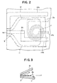
- FIG. 2 is a schematic plan view
- Fig. 3 is a schematic illustration of an essential part.
- a first and second thin-film magnetic cores 11 and 12 are laminated so as to form a magnetic gap g between front end portions thereof so that the magnetic gap g is exposed to a contacting or facing surface in relation to a magnetic recording medium, e.g., an ABS 2 in a flying type magnetic head.
- a magnetic recording medium e.g., an ABS 2 in a flying type magnetic head.
- the composite type thin-film magnetic head is constituted of an inductive type recording magnetic head wherein a closed magnetic path is formed by the first and second thin-film magnetic cores 11 and 12 with the magnetic gap g formed on the front side thereof, and a head coil 7 is wound around the closed magnetic path, and of an MR reproducing magnetic head wherein the first and second thin-film magnetic cores 11 and 12 serve as a magnetic shield, and an MR magnetic sensing element 3 extends rearwardly from the magnetic gap g so as to receive a signal magnetic field based on recorded magnetization given from the magnetic recording medium to the magnetic gap g.
- ⁇ 1 an angle defined between the first thin-film magnetic core 11 and a surface of the MR magnetic sensing element 3 extending in a longitudinal direction x thereof is represented by ⁇ 1
- ⁇ 2 an angle defined between the second thin-film magnetic core 12 and the surface of the MR magnetic sensing element 3 is represented by ⁇ 2 .
- the relation between both the angles ⁇ 1 and ⁇ 2 is set to ⁇ 1 ⁇ ⁇ 2 .
- the angle ⁇ 1 is set to be larger than an angle of the surface of the MR magnetic sensing element 3 with respect to the longitudinal direction x thereof, that is, the angle ⁇ 1 is set to ⁇ 1 > 0°.
- the angle ⁇ 2 is set to 0° ⁇ ⁇ 2 ⁇ 90°.
- the spacing between the first and second thin-film magnetic cores 11 and 12 is gradually increased in a disposed area of a longitudinally middle portion of the MR magnetic sensing element 3 as a distance from the magnetic gap g in the rearward direction increases.
- the formation of the bias conductor for the MR magnetic sensing element 3 as mentioned with reference to Fig. 5 is omitted.
- a desired current is supplied to the head coil 7 to thereby generate a magnetic flux shown by dashed arrows a in Figs. 1 and 3 in the magnetic gap g between the first and second thin-film magnetic cores 11 and 12.
- the spacing between the first and second thin film magnetic cores 11 and 12 in the forming area of the MR magnetic sensing element 3 is increased as the distance from the magnetic gap g in the rearward direction increases, under the condition of ⁇ 1 ⁇ ⁇ 2 , a component of the magnetic flux (magnetic field) in the magnetic gap g is generated in the direction x, that is, in the rearward direction of the MR magnetic sensing element 3.
- a desired external bias magnetic field can be applied to the MR magnetic sensing element 3.
- a desired bias magnetic field can be applied to the MR magnetic sensing element 3. Accordingly, the MR magnetic sensing element 3 can be operated in the range such that a magneto-resistance characteristic with a superior linearity and sensitivity is indicated.
- bias conductor 6 employed in the prior art shown in Figs. 5 and 6 can be omitted, an area to be occupied by the bias conductor 6 and an area to be occupied by the terminal leading portions 16a and 16b extending from the opposite ends of the bias conductor 6 can be accordingly omitted.
- the structure can be simplified, and a total occupied area can be reduced. Accordingly, the general construction can be reduced in size, and the manufacturing step can be simplified.
- the composite type thin-film magnetic head of the present invention is constituted of an MR magnetic reproducing magnetic head and an inductive type recording magnetic head.
- the MR type reproducing magnetic head is constructed so that a bias magnetic field to be applied to the MR magnetic sensing element 3 is obtained as a magnetic field generated by using the head coil 7 as an induction coil of the inductive type recording magnetic head.
- the bias conductor employed in the prior art for applying a bias magnetic field to the MR magnetic sensing element 3 of the MR type reproducing magnetic head can be omitted.
- the terminal leading portions extending from the bias conductor can also be omitted.
- a total occupied area can be reduced, thereby realizing a simple construction and easy manufacturing and improving the reliability of the composite type thin-film magnetic head.
- a first thin-film magnetic core 11 of FeNi or the like is formed with a desired pattern by flame plating or the like as known in the art on a substrate 1 constructed of a slider itself of Al 2 O 3 ⁇ TiC or the like, which constitutes a flying type magnetic head, or a similar non-magnetic base plate mounted on the slider, under the condition where a desired external magnetic field is applied.
- the desired pattern is formed by removing a photoresist, for example, and etching an undesired peripheral portion.
- a non-magnetic insulating layer 20 of SiO 2 , Al 2 O 3 or the like is so formed as to embed the first thin-film magnetic core 11 by sputtering or the like.
- an MR magnetic sensing element 3 is formed on the surface of the insulating layer 20.
- Fig. 4 illustrates a schematic section of the MR magnetic sensing element 3 by way of example.
- the MR magnetic sensing element 3 has a laminated structure such that first and second MR thin films 3A and 3B are magneto-statically connected with each other through a non-magnetic insulating thin film 23 of SiO 2 or the like. With this structure, generation of magnetic domain walls can be avoided to thereby reduce Barkhausen noise.
- the MR thin films 3A and 3B constituting the MR magnetic sensing element 3 are laminated together, through the non-magnetic insulating layer 23 so as to extend rearwardly along the first thin-film magnetic core 11 from its front end, that is, in a direction x representing a depth direction of a magnetic gap g to be hereinafter, described.
- Two electrodes 4a and 4b formed from thin-film conductive layers are electrically connected to opposite ends of the MR thin films 3A and 3B of the MR magnetic sensing element 3, and terminal leading portions 14a and 14b are so formed as to extend from the electrodes 4a and 4b, respectively.
- a head coil 7 having a desired pattern of a thin-film conductive layer is formed simultaneously with the formation of the electrodes 4a and 4b and the terminal leading portions 17a and 17b or in a different step.
- an insulating layer 20 (cf fig. 1) of SiO 2 or the like is formed by sputtering or the like so as to entirely cover all the electrodes 4a and 4b, the MR magnetic sensing element 3, the head coil 7, etc.
- the insulating layer 20 is partially inclined at an angle ⁇ 2 so that a thickness thereof is gradually increased in a forming area of the MR magnetic sensing element 3 as a distance from a front end of the MR magnetic sensing element 3 in the rearward direction increases.
- the insulating layer 20 is perforated by selective etching using photolithography to form a window at a central portion of the head coil 7.
- a second thin-film magnetic core 12 is so formed as to be connected through the window to the first thin-film magnetic core 11, thus effecting magnetic connection between the first and second thin-film magnetic cores 11 and 12.
- the second thin-film magnetic core 12 is formed with a pattern such that a width thereof is small at its front end, and is gradually increased as a distance from the front end in the rearward direction increases.
- the magnetic gap g having a desired spacing or a gap length is formed between the front ends of the first and second thin-film magnetic cores 11 and 12. Further, the first and second thin-film magnetic cores 11 and 12 are arranged so that a spacing therebetween in the forming area of the MR magnetic sensing element 3 on the rear side of the magnetic gap g is gradually increased under the conditions that an angle ⁇ 1 defined between the first thin-film magnetic core 11 and a surface of the MR magnetic sensing element 3 extending in the direction x and an angle ⁇ 2 defined between the second thin-film magnetic core 12 and the surface of the MR magnetic sensing element 3 are related to each other so as to satisfy ⁇ 1 ⁇ ⁇ 2 , ⁇ 1 > 0°, and 0° ⁇ ⁇ 2 ⁇ 90°, preferably 30° ⁇ ⁇ 2 ⁇ 90°.
- a terminal leading portion 17a with a desired pattern of a thin-film conductive layer extends from an outer end of the head coil 7 having a spiral pattern, for example, and a terminal leading portion 17b with a desired pattern of a thin-film conductive layer extends from an inner end of the head coil 7 through a window formed in the insulating layer 20.
- the front end surface of the composite type thin-film magnetic head having the above construction is polished together with the front end surface of the substrate 1 to form an ABS 2 as a flat contacting or facing surface in relation to a magnetic recording medium, so that the front end of the magnetic gap g is exposed to the ABS 2.
- a desired current with a signal current superimposed according to a desired recording information is supplied to the head coil 7 to generate a magnetic flux in a closed magnetic path formed by the first thin-film magnetic core 11 and the second thin-film magnetic core 12 and apply the magnetic field from the magnetic gap g to the magnetic recording medium, thus effecting recording of the information.
- a predetermined sensing current is applied between both the electrodes 4a and 4b of the MR magnetic sensing element 3 (i.e., between both the terminal leading portions 14a and 14b). More specifically, as shown in Fig.
- a predetermined sensing current i s /2 is supplied to each of the MR thin films 3A and 3B constituting the MR magnetic sensing element 3 in the depth direction of the magnetic gap g.
- a desired direct current is supplied to the head coil 7.
- an external bias magnetic field along the flowing direction of the sensing current in the MR magnetic sensing element 3 is generated as shown by dashed arrows a in Figs. 1 and 3, thus obtaining a desired bias magnetized condition of the MR magnetic sensing element 3.
- each portion of the composite type thin-film magnetic head as mentioned above may be changed or modified within the scope of the present invention.
- the head coil 7 is formed from a single layer thin film having a spiral pattern in the above preferred embodiment, it may be constructed as a multilayer structure having a plurality of thin-film layers laminated together through insulating layers and connected together at groove portions.
Landscapes
- Engineering & Computer Science (AREA)
- Manufacturing & Machinery (AREA)
- Magnetic Heads (AREA)
Claims (3)
- Zusammengesetzter Dünnfilmmagnetkopf aus einem Dünnfilmmagnetkopf vom Typ mit Magnetowiderstandseffekt und einem induktiven Dünnfilmmagnetkopf, mit:- einem ersten Dünnfilmmagnetkern (11);- einem zweiten Dünnfilmmagnetkern (12), der so auf den ersten Dünnfilmmagnetkern (11) laminiert ist, dass zwischen den Vorderendbereichen des ersten und zweiten Dünnfilmmagnetkerns ein Magnetspalt (g) ausgebildet ist, der an einer kontaktierenden oder zugewandten Fläche (2) in bezug auf einen magnetischen Aufzeichnungsträger freiliegt;- einem magnetischen Abtastelement (3) vom Typ mit Magnetowiderstandseffekt, das im Magnetspalt (g) angeordnet ist und sich ausgehend von diesem in rückwärtiger Richtung (x) erstreckt; und- einer Kopfspule (7), die an der Rückseite des magnetischen Magnetowiderstands-Abtastelements um einen durch den ersten und zweiten Dünnfilmmagnetkern gebildeten Magnetpfad gewickelt ist;- wobei der Abstand zwischen den Vorderendbereichen des ersten und zweiten Dünnfilmmagnetkerns im Bereich, in dem das magnetische Magnetowiderstands-Abtastelement (3) angeordnet ist, allmählich mit zunehmendem Abstand vom Magnetspalt (g) in rückwärtiger Richtung (x) zunimmt;- wobei ein Winkel Θ1, der zwischen dem ersten Dünnfilmmagnetkern (11) und dem magnetischen Magnetowiderstands-Abtastelement (3) gebildet ist, und ein anderer Winkel Θ2, der zwischen dem zweiten Dünnfilmmagnetkern (12) und dem magnetischen Magnetowiderstands-Abtastelement (3) gebildet ist, so miteinander in Beziehung stehen, dass sie die Bedingung Θ1 ≠ Θ2 erfüllen;dadurch gekennzeichnet, dass- der Winkel Θ1 auf 0° < Θ1 eingestellt ist und der Winkel Θ2 auf 0° < Θ2 eingestellt ist;- das magnetische Magnetowiderstands-Abtastelement (3) ein Laminat aus einem ersten Magnetowiderstands-Dünnfilm (3A) und einem zweiten Magnetowiderstands-Dünnfilm (3B), der über einen unmagnetischen, isolierenden Dünnfilm (23) magnetostatisch mit dem ersten Magnetowiderstands-Dünnfilm (3A) verbunden ist, ist; und- zwei Elektroden (4a, 4b), die aus leitenden Dünnfilmschichten bestehen, elektrisch an entgegengesetzten Enden des ersten und zweiten Magnetowiderstands-Dünnfilms (3A, 3B) angeschlossen sind.
- Zusammengesetzter Dünnfilmmagnetkopf nach Anspruch 1, bei dem der Winkel Θ2 auf 0° < Θ2 ≤ 90° eingestellt ist.
- Zusammengesetzter Dünnfilmmagnetkopf nach Anspruch 2, bei dem der Winkel Θ2 auf 30° ≤ Θ2 ≤ 90° eingestellt ist.
Applications Claiming Priority (2)
| Application Number | Priority Date | Filing Date | Title |
|---|---|---|---|
| JP28687790A JPH04159606A (ja) | 1990-10-24 | 1990-10-24 | 複合型薄膜磁気ヘッド |
| JP286877/90 | 1990-10-24 |
Publications (3)
| Publication Number | Publication Date |
|---|---|
| EP0482642A2 EP0482642A2 (de) | 1992-04-29 |
| EP0482642A3 EP0482642A3 (en) | 1994-06-08 |
| EP0482642B1 true EP0482642B1 (de) | 1997-01-08 |
Family
ID=17710162
Family Applications (1)
| Application Number | Title | Priority Date | Filing Date |
|---|---|---|---|
| EP19910118167 Expired - Lifetime EP0482642B1 (de) | 1990-10-24 | 1991-10-24 | Zusammengesetzter magnetoresistiver Dünnfilmmagnetkopf |
Country Status (3)
| Country | Link |
|---|---|
| EP (1) | EP0482642B1 (de) |
| JP (1) | JPH04159606A (de) |
| DE (1) | DE69124059T2 (de) |
Families Citing this family (4)
| Publication number | Priority date | Publication date | Assignee | Title |
|---|---|---|---|---|
| JP2780916B2 (ja) * | 1993-12-08 | 1998-07-30 | 富士通株式会社 | 垂直磁気記録用磁気ヘッド |
| US5557491A (en) * | 1994-08-18 | 1996-09-17 | International Business Machines Corporation | Two terminal single stripe orthogonal MR head having biasing conductor integral with the lead layers |
| US5923502A (en) * | 1995-12-21 | 1999-07-13 | International Business Machines Corporation | Magneto-resistive head including a selectively placed low-reluctance path between shields |
| JP3151155B2 (ja) * | 1996-09-10 | 2001-04-03 | アルプス電気株式会社 | 薄膜磁気ヘッド |
Family Cites Families (5)
| Publication number | Priority date | Publication date | Assignee | Title |
|---|---|---|---|---|
| JPS5654621A (en) * | 1979-10-05 | 1981-05-14 | Nec Corp | Thin-film magnetic head |
| US4356523A (en) * | 1980-06-09 | 1982-10-26 | Ampex Corporation | Narrow track magnetoresistive transducer assembly |
| US4547824A (en) * | 1982-12-17 | 1985-10-15 | International Business Machines Corporation | Dual biasing for integrated inductive MR head |
| JPS6258410A (ja) * | 1985-09-09 | 1987-03-14 | Sony Corp | 磁気抵抗効果型磁気ヘツド |
| JPS6258411A (ja) * | 1985-09-09 | 1987-03-14 | Sony Corp | 磁気抵抗効果型磁気ヘツド |
-
1990
- 1990-10-24 JP JP28687790A patent/JPH04159606A/ja active Pending
-
1991
- 1991-10-24 DE DE1991624059 patent/DE69124059T2/de not_active Expired - Fee Related
- 1991-10-24 EP EP19910118167 patent/EP0482642B1/de not_active Expired - Lifetime
Also Published As
| Publication number | Publication date |
|---|---|
| EP0482642A2 (de) | 1992-04-29 |
| DE69124059D1 (de) | 1997-02-20 |
| EP0482642A3 (en) | 1994-06-08 |
| DE69124059T2 (de) | 1997-07-31 |
| JPH04159606A (ja) | 1992-06-02 |
Similar Documents
| Publication | Publication Date | Title |
|---|---|---|
| EP0221540B1 (de) | Den Magnetwiderstandseffekt verwendender Magnetwandlerkopf | |
| US4663685A (en) | Magnetoresistive read transducer having patterned longitudinal bias | |
| EP0881627A2 (de) | Dünnfilmmagnetkopf | |
| EP0269129B1 (de) | Dünnfilmmagnetkopf | |
| JP2002032903A (ja) | 垂直磁気記録用薄膜磁気ヘッド | |
| JPH07262520A (ja) | 薄膜磁気ヘッド | |
| JPH07272225A (ja) | 磁気抵抗性ヘッド | |
| US7207099B2 (en) | Method of manufacturing thin-film magnetic head having a magnetism intercepting layer provided between read head and write head | |
| US6718623B2 (en) | Magnetoresistive device and method of manufacturing same, and thin-film magnetic head and method of manufacturing same | |
| US6369992B1 (en) | Yoke-type head with magneto-resistance effect film recessed from medium facing surface and extending across magnetic gap | |
| EP0482642B1 (de) | Zusammengesetzter magnetoresistiver Dünnfilmmagnetkopf | |
| US6842314B2 (en) | Magnetoresistive device and method of manufacturing same, and thin-film magnetic head and method of manufacturing same | |
| JPH08235542A (ja) | 磁気抵抗効果素子 | |
| JP2718242B2 (ja) | 磁気抵抗効果ヘッド | |
| JPH04137212A (ja) | 磁気抵抗効果磁気ヘッド | |
| JP3082347B2 (ja) | 磁気抵抗効果型薄膜磁気ヘッド | |
| JP4010702B2 (ja) | 薄膜磁気ヘッドの製造方法 | |
| JPH05143938A (ja) | 磁気抵抗効果型磁気ヘツド | |
| JPH07153022A (ja) | 薄膜磁気ヘッド | |
| JPH0546943A (ja) | 薄膜磁気ヘツド | |
| JP3538028B2 (ja) | 薄膜磁気ヘッドおよびその製造方法 | |
| JP2002373405A (ja) | 磁気検出素子、磁気検出素子の製造方法及び磁気ヘッド | |
| JPS6371914A (ja) | 再生ヘツド | |
| JPH0540920A (ja) | 複合型磁気ヘツド及びその製造方法 | |
| JPH07176020A (ja) | 磁気抵抗効果ヘッド及びその製造方法 |
Legal Events
| Date | Code | Title | Description |
|---|---|---|---|
| PUAI | Public reference made under article 153(3) epc to a published international application that has entered the european phase |
Free format text: ORIGINAL CODE: 0009012 |
|
| AK | Designated contracting states |
Kind code of ref document: A2 Designated state(s): DE FR GB |
|
| PUAL | Search report despatched |
Free format text: ORIGINAL CODE: 0009013 |
|
| AK | Designated contracting states |
Kind code of ref document: A3 Designated state(s): DE FR GB |
|
| 17P | Request for examination filed |
Effective date: 19941108 |
|
| 17Q | First examination report despatched |
Effective date: 19950526 |
|
| GRAG | Despatch of communication of intention to grant |
Free format text: ORIGINAL CODE: EPIDOS AGRA |
|
| GRAH | Despatch of communication of intention to grant a patent |
Free format text: ORIGINAL CODE: EPIDOS IGRA |
|
| GRAH | Despatch of communication of intention to grant a patent |
Free format text: ORIGINAL CODE: EPIDOS IGRA |
|
| GRAA | (expected) grant |
Free format text: ORIGINAL CODE: 0009210 |
|
| AK | Designated contracting states |
Kind code of ref document: B1 Designated state(s): DE FR GB |
|
| REF | Corresponds to: |
Ref document number: 69124059 Country of ref document: DE Date of ref document: 19970220 |
|
| ET | Fr: translation filed | ||
| PLBE | No opposition filed within time limit |
Free format text: ORIGINAL CODE: 0009261 |
|
| STAA | Information on the status of an ep patent application or granted ep patent |
Free format text: STATUS: NO OPPOSITION FILED WITHIN TIME LIMIT |
|
| 26N | No opposition filed | ||
| PGFP | Annual fee paid to national office [announced via postgrant information from national office to epo] |
Ref country code: FR Payment date: 20011010 Year of fee payment: 11 |
|
| PGFP | Annual fee paid to national office [announced via postgrant information from national office to epo] |
Ref country code: GB Payment date: 20011024 Year of fee payment: 11 |
|
| PGFP | Annual fee paid to national office [announced via postgrant information from national office to epo] |
Ref country code: DE Payment date: 20011105 Year of fee payment: 11 |
|
| REG | Reference to a national code |
Ref country code: GB Ref legal event code: IF02 |
|
| PG25 | Lapsed in a contracting state [announced via postgrant information from national office to epo] |
Ref country code: GB Free format text: LAPSE BECAUSE OF NON-PAYMENT OF DUE FEES Effective date: 20021024 |
|
| PG25 | Lapsed in a contracting state [announced via postgrant information from national office to epo] |
Ref country code: DE Free format text: LAPSE BECAUSE OF NON-PAYMENT OF DUE FEES Effective date: 20030501 |
|
| GBPC | Gb: european patent ceased through non-payment of renewal fee |
Effective date: 20021024 |
|
| PG25 | Lapsed in a contracting state [announced via postgrant information from national office to epo] |
Ref country code: FR Free format text: LAPSE BECAUSE OF NON-PAYMENT OF DUE FEES Effective date: 20030630 |
|
| REG | Reference to a national code |
Ref country code: FR Ref legal event code: ST |