EP0481093A1 - Circuit de temporisation - Google Patents
Circuit de temporisation Download PDFInfo
- Publication number
- EP0481093A1 EP0481093A1 EP91908785A EP91908785A EP0481093A1 EP 0481093 A1 EP0481093 A1 EP 0481093A1 EP 91908785 A EP91908785 A EP 91908785A EP 91908785 A EP91908785 A EP 91908785A EP 0481093 A1 EP0481093 A1 EP 0481093A1
- Authority
- EP
- European Patent Office
- Prior art keywords
- delay
- drain
- circuit
- type mosfet
- delay time
- Prior art date
- Legal status (The legal status is an assumption and is not a legal conclusion. Google has not performed a legal analysis and makes no representation as to the accuracy of the status listed.)
- Withdrawn
Links
Images

Classifications
-
- H—ELECTRICITY
- H03—ELECTRONIC CIRCUITRY
- H03K—PULSE TECHNIQUE
- H03K5/00—Manipulating of pulses not covered by one of the other main groups of this subclass
- H03K5/01—Shaping pulses
- H03K5/04—Shaping pulses by increasing duration; by decreasing duration
- H03K5/06—Shaping pulses by increasing duration; by decreasing duration by the use of delay lines or other analogue delay elements
-
- H—ELECTRICITY
- H03—ELECTRONIC CIRCUITRY
- H03K—PULSE TECHNIQUE
- H03K5/00—Manipulating of pulses not covered by one of the other main groups of this subclass
- H03K5/13—Arrangements having a single output and transforming input signals into pulses delivered at desired time intervals
- H03K5/133—Arrangements having a single output and transforming input signals into pulses delivered at desired time intervals using a chain of active delay devices
-
- H—ELECTRICITY
- H03—ELECTRONIC CIRCUITRY
- H03K—PULSE TECHNIQUE
- H03K5/00—Manipulating of pulses not covered by one of the other main groups of this subclass
- H03K5/13—Arrangements having a single output and transforming input signals into pulses delivered at desired time intervals
-
- H—ELECTRICITY
- H03—ELECTRONIC CIRCUITRY
- H03K—PULSE TECHNIQUE
- H03K5/00—Manipulating of pulses not covered by one of the other main groups of this subclass
- H03K2005/00013—Delay, i.e. output pulse is delayed after input pulse and pulse length of output pulse is dependent on pulse length of input pulse
- H03K2005/00078—Fixed delay
- H03K2005/0013—Avoiding variations of delay due to power supply
Definitions
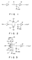
- T1 and T2 are complementary MOSFETs (Metal Oxide Semiconductor Field Effect Transistors) which are used as voltage control type resistances.
- V p and V n are delay control inputs.
- a delay circuit which comprises a first N-type MOSFET having a gate to which a first delay time control voltage is applied and a source connected to a low potential power source; a first P-type MOSFET having a gate to which a second delay time control voltage is applied and a source connected to a high potential power source; a second N-type MOSFET having a gate to which an input signal is supplied and a source to which a drain of the first N-type MOSFET is connected; a second P-type MOSFET having a gate and drain which are connected respectively to the gate and drain of the second N-type MOSFET, and a source connected to the drain of the first P-type MOSFET; and a capacitor having two ends, one end being connected to the node between the drain of the second N-type MOSFET and the drain of the second P-type MOSFET, and the other end being connected to one of the low potential power source and the high potential power source.
- This delay circuit is characterized in that a delay output signal is extracted from the aforementioned one end of the capacitor. Further, according to the present invention, the delay circuit is characterized in that a waveform shaping circuit is connected to one end of the capacitor, and the delay output signal is subjected to waveform shaping in the waveform shaping circuit.
- the drain currents of the resistance MOSFETs When the drain currents of the resistance MOSFETs are increased, the driving capacity of the CMOS inverter is increased, as a result of which rounding of the waveform of the output from the CMOS inverter is reduced, shortening the delay time of the CMOS inverter.
- the drain currents of the resistance MOSFETs can be changed, whereby the delay time of the CMOS inverter can be adjusted.
- the sources of the resistance MOSFETs are connected to power sources such that the potentials are fixed. Therefore, there is no influence by disturbances.
- Fig. 3 is the diagram showing the circuit according to the above embodiment. A part of this circuit and the corresponding part of a conventional circuit are denoted by the same reference numeral.
- a delay time control voltage V n is applied to the gate of an N-type MOS transistor 21, and the source thereof is connected to a ground GND which is used as a low power source potential V ss .
- a delay time control voltage V p is applied to the gate of a P-type MOS transistor 22, and the source thereof is connected to a power source terminal 25 which is used as a positive high power source potential V dd .
- An input signal IN is supplied to the gate of an N-type MOS transistor 23, and the source thereof is connected to the drain of the transistor 21.
- the control voltages V n and V p are decreased and increased, thereby decreasing the drain current which flows through the MOS transistor 22 into the capacitor C and the drain current which flows from the capacitor C through the MOS transistor 21, as a result of which the driving capacity of the CMOS inverter 26 is decreased, increasing the rounding of the waveform of the output therefrom.
- the output from the resistor circuit R i.e., the output from the CMOS inverter 26, is input to the waveform shaping CMOS inverter 12 and subjected to waveform shaping so as to eliminate the rounding used for the aforementioned delay, and is thereafter extracted as the delay output OUT.
- Fig. 4 is a circuit diagram showing a concrete circuit which constitutes the waveform shaping CMOS inverter 12.
- the CMOS inverter 12 includes an N-type MOS transistor 31 and a P-type MOS transistor 32 which are connected in series between the ground and the high potential power source V dd .
Abstract
L'invention se rapporte à un circuit de temporisation, dans lequel des transistors MOS (21, 22) pour résistances servant à commander la durée de temporisation d'un inverseur CMOS (26) sont insérés entre la source de l'inverseur CMOS (26) et les potentiels d'alimentation (GND, Vdd), et les sources correspondantes des transistors MOS (21, 22) sont connectées respectivement aux potentiels d'alimentation (GND, Vdd). Ainsi, en modifiant les courants de drain des transistors MOS (21, 22), on modifie respectivement leurs tensions de commande (Vn, Vp). La capacité de commande de l'inverseur CMOS (26) est modifiée en conséquence, ce qui permet de réguler la durée de temporisation de l'inverseur (26). En outre, étant donné que les sources des transistors MOS (21, 22) sont connectées aux potentiels d'alimentation (potentiels fixes) (GND, Vdd) respectivement, on obtient la stabilité de la durée de temporisation même en cas de perturbations.
Applications Claiming Priority (2)
| Application Number | Priority Date | Filing Date | Title |
|---|---|---|---|
| JP2115204A JPH0413305A (ja) | 1990-05-02 | 1990-05-02 | 遅延回路 |
| JP115204/90 | 1990-05-02 |
Publications (2)
| Publication Number | Publication Date |
|---|---|
| EP0481093A1 true EP0481093A1 (fr) | 1992-04-22 |
| EP0481093A4 EP0481093A4 (en) | 1992-08-26 |
Family
ID=14656936
Family Applications (1)
| Application Number | Title | Priority Date | Filing Date |
|---|---|---|---|
| EP19910908785 Withdrawn EP0481093A4 (en) | 1990-05-02 | 1991-05-01 | Delay circuit |
Country Status (4)
| Country | Link |
|---|---|
| EP (1) | EP0481093A4 (fr) |
| JP (1) | JPH0413305A (fr) |
| KR (1) | KR910021019A (fr) |
| WO (1) | WO1991017602A1 (fr) |
Cited By (4)
| Publication number | Priority date | Publication date | Assignee | Title |
|---|---|---|---|---|
| US5559476A (en) * | 1995-05-31 | 1996-09-24 | Cirrus Logic, Inc. | Voltage controlled oscillator including voltage controlled delay circuit with power supply noise isolation |
| EP0768759A2 (fr) * | 1995-10-11 | 1997-04-16 | Nec Corporation | Circuit de retard analogique |
| EP0840451A1 (fr) * | 1996-10-30 | 1998-05-06 | STMicroelectronics S.r.l. | Circuit générateur pour générer des signaux sans chevauchement |
| CN102299701A (zh) * | 2011-08-23 | 2011-12-28 | 北京兆易创新科技有限公司 | 延时单元电路 |
Families Citing this family (4)
| Publication number | Priority date | Publication date | Assignee | Title |
|---|---|---|---|---|
| KR100453886B1 (ko) * | 1997-07-29 | 2004-12-17 | 삼성전자주식회사 | 링 오실레이터 |
| JP3586612B2 (ja) * | 2000-03-08 | 2004-11-10 | エルピーダメモリ株式会社 | 遅延回路 |
| JPWO2007114379A1 (ja) * | 2006-03-31 | 2009-08-20 | 株式会社アドバンテスト | 可変遅延回路、試験装置および電子デバイス |
| JP6819115B2 (ja) * | 2016-07-25 | 2021-01-27 | セイコーエプソン株式会社 | コンパレーター、回路装置、物理量センサー、電子機器及び移動体 |
Family Cites Families (4)
| Publication number | Priority date | Publication date | Assignee | Title |
|---|---|---|---|---|
| JPS6139722A (ja) * | 1984-07-31 | 1986-02-25 | Nippon Gakki Seizo Kk | 遅延時間安定化回路 |
| JPS62214716A (ja) * | 1986-03-14 | 1987-09-21 | Matsushita Electric Ind Co Ltd | Cmos可変遅延線 |
| GB2197553A (en) * | 1986-10-07 | 1988-05-18 | Western Digital Corp | Phase-locked loop delay line |
| JPS63266919A (ja) * | 1987-04-24 | 1988-11-04 | Hitachi Ltd | 半導体集積回路装置 |
-
1990
- 1990-05-02 JP JP2115204A patent/JPH0413305A/ja active Pending
-
1991
- 1991-04-29 KR KR1019910006848A patent/KR910021019A/ko not_active IP Right Cessation
- 1991-05-01 WO PCT/JP1991/000595 patent/WO1991017602A1/fr not_active Application Discontinuation
- 1991-05-01 EP EP19910908785 patent/EP0481093A4/en not_active Withdrawn
Non-Patent Citations (2)
| Title |
|---|
| No further relevant documents disclosed * |
| See also references of WO9117602A1 * |
Cited By (5)
| Publication number | Priority date | Publication date | Assignee | Title |
|---|---|---|---|---|
| US5559476A (en) * | 1995-05-31 | 1996-09-24 | Cirrus Logic, Inc. | Voltage controlled oscillator including voltage controlled delay circuit with power supply noise isolation |
| EP0768759A2 (fr) * | 1995-10-11 | 1997-04-16 | Nec Corporation | Circuit de retard analogique |
| EP0768759A3 (fr) * | 1995-10-11 | 1998-03-18 | Nec Corporation | Circuit de retard analogique |
| EP0840451A1 (fr) * | 1996-10-30 | 1998-05-06 | STMicroelectronics S.r.l. | Circuit générateur pour générer des signaux sans chevauchement |
| CN102299701A (zh) * | 2011-08-23 | 2011-12-28 | 北京兆易创新科技有限公司 | 延时单元电路 |
Also Published As
| Publication number | Publication date |
|---|---|
| JPH0413305A (ja) | 1992-01-17 |
| KR910021019A (ko) | 1991-12-20 |
| WO1991017602A1 (fr) | 1991-11-14 |
| EP0481093A4 (en) | 1992-08-26 |
Similar Documents
| Publication | Publication Date | Title |
|---|---|---|
| EP0648388B1 (fr) | Oscillateur en quadrature | |
| US6172535B1 (en) | High-speed analog comparator structures and methods | |
| JPH0113766B2 (fr) | ||
| KR100236058B1 (ko) | 트리거 전압 조정이 가능한 슈미트 트리거 회로 | |
| KR19990037988A (ko) | 지연회로 | |
| US5057722A (en) | Delay circuit having stable delay time | |
| EP0463854A1 (fr) | Circuit d'attaque d'horloge | |
| CA1047602A (fr) | Circuit de conversion de niveau de tension | |
| JPH04313907A (ja) | 信号処理装置 | |
| EP0481093A1 (fr) | Circuit de temporisation | |
| JPH10209781A (ja) | 差動回路を含む電子回路 | |
| KR100576716B1 (ko) | 출력 전류의 왜곡이 보상된 트랜스컨덕터 회로 | |
| US7068090B2 (en) | Amplifier circuit | |
| US6111456A (en) | Semiconductor circuit | |
| US5604448A (en) | Output buffer circuit having low noise characteristics | |
| KR900007036B1 (ko) | 필터회로 | |
| EP0722221A2 (fr) | Circuit commutateur de courant à fonctionnement rapide sans fourniture externe de polarisation de référence | |
| EP0417985A2 (fr) | Amplificateur inverseur à amplitude stabilisée | |
| JPH118534A (ja) | 半導体集積回路 | |
| KR20050064114A (ko) | 출력 전류의 왜곡이 보상된 트랜스컨덕터 회로 | |
| EP0994564A1 (fr) | Circuit inverseur avec contrôle du rapport cyclique | |
| JPH0317244B2 (fr) | ||
| KR19980041577A (ko) | 지연회로 | |
| US7622964B2 (en) | Analog buffer circuit | |
| US5296754A (en) | Push-pull circuit resistant to power supply and temperature induced distortion |
Legal Events
| Date | Code | Title | Description |
|---|---|---|---|
| PUAI | Public reference made under article 153(3) epc to a published international application that has entered the european phase |
Free format text: ORIGINAL CODE: 0009012 |
|
| 17P | Request for examination filed |
Effective date: 19920102 |
|
| AK | Designated contracting states |
Kind code of ref document: A1 Designated state(s): DE FR GB |
|
| A4 | Supplementary search report drawn up and despatched |
Effective date: 19920706 |
|
| AK | Designated contracting states |
Kind code of ref document: A4 Designated state(s): DE FR GB |
|
| STAA | Information on the status of an ep patent application or granted ep patent |
Free format text: STATUS: THE APPLICATION HAS BEEN WITHDRAWN |
|
| 18W | Application withdrawn |
Withdrawal date: 19930602 |