EP0481093A1 - Delay circuit - Google Patents
Delay circuit Download PDFInfo
- Publication number
- EP0481093A1 EP0481093A1 EP91908785A EP91908785A EP0481093A1 EP 0481093 A1 EP0481093 A1 EP 0481093A1 EP 91908785 A EP91908785 A EP 91908785A EP 91908785 A EP91908785 A EP 91908785A EP 0481093 A1 EP0481093 A1 EP 0481093A1
- Authority
- EP
- European Patent Office
- Prior art keywords
- delay
- drain
- circuit
- type mosfet
- delay time
- Prior art date
- Legal status (The legal status is an assumption and is not a legal conclusion. Google has not performed a legal analysis and makes no representation as to the accuracy of the status listed.)
- Withdrawn
Links
Images

Classifications
-
- H—ELECTRICITY
- H03—ELECTRONIC CIRCUITRY
- H03K—PULSE TECHNIQUE
- H03K5/00—Manipulating of pulses not covered by one of the other main groups of this subclass
- H03K5/01—Shaping pulses
- H03K5/04—Shaping pulses by increasing duration; by decreasing duration
- H03K5/06—Shaping pulses by increasing duration; by decreasing duration by the use of delay lines or other analogue delay elements
-
- H—ELECTRICITY
- H03—ELECTRONIC CIRCUITRY
- H03K—PULSE TECHNIQUE
- H03K5/00—Manipulating of pulses not covered by one of the other main groups of this subclass
- H03K5/13—Arrangements having a single output and transforming input signals into pulses delivered at desired time intervals
- H03K5/133—Arrangements having a single output and transforming input signals into pulses delivered at desired time intervals using a chain of active delay devices
-
- H—ELECTRICITY
- H03—ELECTRONIC CIRCUITRY
- H03K—PULSE TECHNIQUE
- H03K5/00—Manipulating of pulses not covered by one of the other main groups of this subclass
- H03K5/13—Arrangements having a single output and transforming input signals into pulses delivered at desired time intervals
-
- H—ELECTRICITY
- H03—ELECTRONIC CIRCUITRY
- H03K—PULSE TECHNIQUE
- H03K5/00—Manipulating of pulses not covered by one of the other main groups of this subclass
- H03K2005/00013—Delay, i.e. output pulse is delayed after input pulse and pulse length of output pulse is dependent on pulse length of input pulse
- H03K2005/00078—Fixed delay
- H03K2005/0013—Avoiding variations of delay due to power supply
Definitions
- T1 and T2 are complementary MOSFETs (Metal Oxide Semiconductor Field Effect Transistors) which are used as voltage control type resistances.
- V p and V n are delay control inputs.
- a delay circuit which comprises a first N-type MOSFET having a gate to which a first delay time control voltage is applied and a source connected to a low potential power source; a first P-type MOSFET having a gate to which a second delay time control voltage is applied and a source connected to a high potential power source; a second N-type MOSFET having a gate to which an input signal is supplied and a source to which a drain of the first N-type MOSFET is connected; a second P-type MOSFET having a gate and drain which are connected respectively to the gate and drain of the second N-type MOSFET, and a source connected to the drain of the first P-type MOSFET; and a capacitor having two ends, one end being connected to the node between the drain of the second N-type MOSFET and the drain of the second P-type MOSFET, and the other end being connected to one of the low potential power source and the high potential power source.
- This delay circuit is characterized in that a delay output signal is extracted from the aforementioned one end of the capacitor. Further, according to the present invention, the delay circuit is characterized in that a waveform shaping circuit is connected to one end of the capacitor, and the delay output signal is subjected to waveform shaping in the waveform shaping circuit.
- the drain currents of the resistance MOSFETs When the drain currents of the resistance MOSFETs are increased, the driving capacity of the CMOS inverter is increased, as a result of which rounding of the waveform of the output from the CMOS inverter is reduced, shortening the delay time of the CMOS inverter.
- the drain currents of the resistance MOSFETs can be changed, whereby the delay time of the CMOS inverter can be adjusted.
- the sources of the resistance MOSFETs are connected to power sources such that the potentials are fixed. Therefore, there is no influence by disturbances.
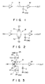
- Fig. 3 is the diagram showing the circuit according to the above embodiment. A part of this circuit and the corresponding part of a conventional circuit are denoted by the same reference numeral.
- a delay time control voltage V n is applied to the gate of an N-type MOS transistor 21, and the source thereof is connected to a ground GND which is used as a low power source potential V ss .
- a delay time control voltage V p is applied to the gate of a P-type MOS transistor 22, and the source thereof is connected to a power source terminal 25 which is used as a positive high power source potential V dd .
- An input signal IN is supplied to the gate of an N-type MOS transistor 23, and the source thereof is connected to the drain of the transistor 21.
- the control voltages V n and V p are decreased and increased, thereby decreasing the drain current which flows through the MOS transistor 22 into the capacitor C and the drain current which flows from the capacitor C through the MOS transistor 21, as a result of which the driving capacity of the CMOS inverter 26 is decreased, increasing the rounding of the waveform of the output therefrom.
- the output from the resistor circuit R i.e., the output from the CMOS inverter 26, is input to the waveform shaping CMOS inverter 12 and subjected to waveform shaping so as to eliminate the rounding used for the aforementioned delay, and is thereafter extracted as the delay output OUT.
- Fig. 4 is a circuit diagram showing a concrete circuit which constitutes the waveform shaping CMOS inverter 12.
- the CMOS inverter 12 includes an N-type MOS transistor 31 and a P-type MOS transistor 32 which are connected in series between the ground and the high potential power source V dd .
Abstract
A delay circuit wherein MOS transistors (21, 22) for resistors for controlling the delay time of a CMOS inverter (26) are inserted between the source of the CMOS inverter (26) and power supply potentials (GND, Vdd) respectively and the respective sources of the MOS transistors (21, 22) are connected with the power supply potentials (GND, Vdd) respectively. Therefore, by changing the drain currents of the MOS transistors (21, 22) the control voltages (Vn, Vp) thereof are changed respectively. The driving capability of the CMOS inverter (26) is consequently changed, allowing the delay time of the inverter (26) to be regulated. Further, since the sources of the MOS transistors (21, 22) are connected with the power supply potentials (fixed potentials) (GND, Vdd) respectively, the delay time being stable even against disturbance is obtained.
Description
- This invention relates to a delay circuit including a MOSFET and which is used particularly in an analog circuit.
- In general, an analog-type delay circuit utilizes delay due to LC (L is an inductance and C is a capacitor) or CR (R is a resistance). Especially in an integrated circuit, it is difficult to form inductance L, and therefore delay due to CR is utilized.
- The principle of a delay circuit having such a structure is shown in Fig. 1. In the case of providing this circuit with a variable delay function, the value of capacitor C or resistance R is varied. In an integrated circuit wherein a MOSFET has a variable delay function, resistance R is constituted by a MOSFET.
Reference numerals - A conventional delay circuit having such a structure is shown in Fig. 2. T₁ and T₂ are complementary MOSFETs (Metal Oxide Semiconductor Field Effect Transistors) which are used as voltage control type resistances. Vp and Vn are delay control inputs.
- However, in a conventional variable delay circuit, the source potentials and drain potentials of an N-type MOSFET (referred to as an N-type MOS transistor) T₁ and a P-type MOSFET (referred to as a P-type MOS transistor) T₂, which are used as resistances, change in accordance with an input signal IN which passes through these MOS transistors, which causes fluctuation of gate and backgate potentials, varying the resistances of the above MOS transistors dynamically.
- Further, when the input signals IN pass through the MOS transistors T₁ and T₂, interference occurs between each of delay control voltages Vp and Vn and the input signal IN, due to a parasitic capacitance between the channel and gate of each of the MOS transistors T₁ and T₂, resulting in a delay time influenced by the input signal. In order to eliminate this influence, the driving impedances of the delay control voltages Vp and Vn should be set at small values. However, obtaining a voltage source having a small driving impedance is difficult in terms of manufacturing techniques. In general, a capacitor is used to attain a small impedance. However, there is a limit to the capacitance of the capacitor which can be formed in an integrated circuit, making it difficult to completely eliminate interference between signals.
- It is therefore the object of the present invention to provide a delay variable type delay circuit wherein a delay time which is stable irrespective of interference between signals can be obtained.
- According to the present invention, there is provided a delay circuit which comprises a first N-type MOSFET having a gate to which a first delay time control voltage is applied and a source connected to a low potential power source; a first P-type MOSFET having a gate to which a second delay time control voltage is applied and a source connected to a high potential power source; a second N-type MOSFET having a gate to which an input signal is supplied and a source to which a drain of the first N-type MOSFET is connected; a second P-type MOSFET having a gate and drain which are connected respectively to the gate and drain of the second N-type MOSFET, and a source connected to the drain of the first P-type MOSFET; and a capacitor having two ends, one end being connected to the node between the drain of the second N-type MOSFET and the drain of the second P-type MOSFET, and the other end being connected to one of the low potential power source and the high potential power source. This delay circuit is characterized in that a delay output signal is extracted from the aforementioned one end of the capacitor. Further, according to the present invention, the delay circuit is characterized in that a waveform shaping circuit is connected to one end of the capacitor, and the delay output signal is subjected to waveform shaping in the waveform shaping circuit.
- To be specific, according to the present invention, resistance MOSFETs (the first N-type MOSFET and the first P-type MOSFET) for controlling the delay time of a CMOS inverter (constituted by the second N-type MOSFET and the second P-type MOSFET) are inserted between the source and power source of the above CMOS inverter. When the drain currents of the aforementioned resistance MOSFETs are decreased by adjusting the first delay time control voltage and the second delay time control voltage which are mentioned above, the driving capacity of the CMOS inverter is decreased, as a result of which rounding of the waveform of the output from the CMOS inverter is increased, prolonging the delay time of the CMOS inverter. When the drain currents of the resistance MOSFETs are increased, the driving capacity of the CMOS inverter is increased, as a result of which rounding of the waveform of the output from the CMOS inverter is reduced, shortening the delay time of the CMOS inverter. Thus, by changing the first delay time control voltage and the second delay time control voltage, the drain currents of the resistance MOSFETs can be changed, whereby the delay time of the CMOS inverter can be adjusted. Further, according to the present invention, the sources of the resistance MOSFETs are connected to power sources such that the potentials are fixed. Therefore, there is no influence by disturbances. In order to eliminate rounding, which is used for adjusting the delay time, from the waveform of the output, that output is extracted as a delay output after being subjected to waveform shaping in the waveform shaping circuit. In addition, the resistance MOSFETs are operated in a saturation state.
-
- Fig. 1 is a diagram showing the principle of a delay circuit;
- Fig. 2 is a diagram showing a conventional voltage control type delay circuit;
- Fig. 3 is a diagram showing the delay circuit according to one embodiment of this invention;
- Fig. 4 is a diagram showing a concrete circuit which constitutes a waveform shaping
CMOS inverter 12 in the delay circuit shown in Fig. 3; and - Fig. 5 is a diagram showing a modification of the delay circuit shown in Fig. 3.
- One embodiment of the present invention will now be described with reference to the drawings.
- Fig. 3 is the diagram showing the circuit according to the above embodiment. A part of this circuit and the corresponding part of a conventional circuit are denoted by the same reference numeral. As shown in this drawing, a delay time control voltage Vn is applied to the gate of an N-
type MOS transistor 21, and the source thereof is connected to a ground GND which is used as a low power source potential Vss. A delay time control voltage Vp is applied to the gate of a P-type MOS transistor 22, and the source thereof is connected to apower source terminal 25 which is used as a positive high power source potential Vdd. An input signal IN is supplied to the gate of an N-type MOS transistor 23, and the source thereof is connected to the drain of thetransistor 21. The gate and drain of a P-type MOS transistor 24 are connected respectively to the gate and drain of thetransistor 23. The above-mentioned connection results in formation of a resistor circuit R having a CMOS inverter structure. In other words, according to the aforementioned structures, A CMOS inverter is constituted by theMOS transistors MOS transistors CMOS inverter 12. - In the case of prolonging a delay time in the delay circuit having the aforementioned structures, the control voltages Vn and Vp are decreased and increased, thereby decreasing the drain current which flows through the
MOS transistor 22 into the capacitor C and the drain current which flows from the capacitor C through theMOS transistor 21, as a result of which the driving capacity of theCMOS inverter 26 is decreased, increasing the rounding of the waveform of the output therefrom. In the case of shortening the delay time, the control voltages Vn and Vp are increased and decreased, thereby increasing the drain current which flows through theMOS transistor 22 into the capacitor C and the drain current which flows from the capacitor C through theMOS transistor 21, as a result of which the drive capacity of theCMOS inverter 26 is increased, reducing the rounding of the waveform of the output therefrom. In any case, theMOS transistors - The output from the resistor circuit R, i.e., the output from the
CMOS inverter 26, is input to the waveform shapingCMOS inverter 12 and subjected to waveform shaping so as to eliminate the rounding used for the aforementioned delay, and is thereafter extracted as the delay output OUT. - In the above-mentioned delay circuit, since the source of each of the
MOS transistors transistors transistors MOS transistor 21 and the gate-drain capacitance of theMOS transistor 22. Therefore, the amount of interference is smaller than in the conventional circuit shown in Fig. 1, which ensures an improved stabilization of the circuit operation for delaying. - Fig. 4 is a circuit diagram showing a concrete circuit which constitutes the waveform shaping
CMOS inverter 12. TheCMOS inverter 12 includes an N-type MOS transistor 31 and a P-type MOS transistor 32 which are connected in series between the ground and the high potential power source Vdd. - The present invention is not limited to the aforementioned embodiment, and various other embodiments can be realized without departing from the scope of this invention. For example, according to the above-mentioned embodiment, the capacitor C is connected to the ground potential. However, it may be connected to the high power source potential Vdd, as shown in Fig. 5.
- The present invention can not only suppress the interference between the input signal and the control signal of the CMOS inverter, but also ensure an operation which is stable irrespective of disturbances. Therefore, the circuit of the present invention is useful when being incorporated into a circuit involving the switching operation which may cause generation of noise.
Claims (2)
- A delay circuit comprising:
a first N-type MOSFET having a gate to which a first delay time control voltage is applied and a source connected to a low potential power source;
a first P-type MOSFET having a gate to which a second delay time control voltage is applied and a source connected to a high potential power source;
a second N-type MOSFET having a gate to which an input signal is supplied and a source to which a drain of the first N-type MOSFET is connected;
a second P-type MOSFET having a gate and drain which are connected respectively to the gate and drain of the second N-type MOSFET, and a source connected to a drain of the first P-type MOSFET; and
a capacitor having two ends, one end being connected to a node between a drain of the second N-type MOSFET and the drain of the second P-type MOSFET, and the other end being connected to one of the low potential power source and the high potential power source;
said delay circuit being characterized in that a delay output signal is extracted from said one end of the capacitor. - The delay circuit according to claim 1, characterized in that a waveform shaping circuit is connected to said one end of the capacitor, and said delay output signal is subjected to waveform shaping in the waveform shaping circuit.
Applications Claiming Priority (2)
| Application Number | Priority Date | Filing Date | Title |
|---|---|---|---|
| JP115204/90 | 1990-05-02 | ||
| JP2115204A JPH0413305A (en) | 1990-05-02 | 1990-05-02 | Delay circuit |
Publications (2)
| Publication Number | Publication Date |
|---|---|
| EP0481093A1 true EP0481093A1 (en) | 1992-04-22 |
| EP0481093A4 EP0481093A4 (en) | 1992-08-26 |
Family
ID=14656936
Family Applications (1)
| Application Number | Title | Priority Date | Filing Date |
|---|---|---|---|
| EP19910908785 Withdrawn EP0481093A4 (en) | 1990-05-02 | 1991-05-01 | Delay circuit |
Country Status (4)
| Country | Link |
|---|---|
| EP (1) | EP0481093A4 (en) |
| JP (1) | JPH0413305A (en) |
| KR (1) | KR910021019A (en) |
| WO (1) | WO1991017602A1 (en) |
Cited By (4)
| Publication number | Priority date | Publication date | Assignee | Title |
|---|---|---|---|---|
| US5559476A (en) * | 1995-05-31 | 1996-09-24 | Cirrus Logic, Inc. | Voltage controlled oscillator including voltage controlled delay circuit with power supply noise isolation |
| EP0768759A2 (en) * | 1995-10-11 | 1997-04-16 | Nec Corporation | Analogue delay circuit |
| EP0840451A1 (en) * | 1996-10-30 | 1998-05-06 | STMicroelectronics S.r.l. | Generator circuit for non overlapping digital signals |
| CN102299701A (en) * | 2011-08-23 | 2011-12-28 | 北京兆易创新科技有限公司 | Time-delay unit circuit |
Families Citing this family (4)
| Publication number | Priority date | Publication date | Assignee | Title |
|---|---|---|---|---|
| KR100453886B1 (en) * | 1997-07-29 | 2004-12-17 | 삼성전자주식회사 | Ring oscillator for generating clock signal with constant frequency regardless of supply voltage |
| JP3586612B2 (en) * | 2000-03-08 | 2004-11-10 | エルピーダメモリ株式会社 | Delay circuit |
| KR101018704B1 (en) * | 2006-03-31 | 2011-03-04 | 가부시키가이샤 어드밴티스트 | Variable delay circuit, testing apparatus and electronic device |
| JP6819115B2 (en) * | 2016-07-25 | 2021-01-27 | セイコーエプソン株式会社 | Comparator, circuit device, physical quantity sensor, electronic device and mobile |
Family Cites Families (4)
| Publication number | Priority date | Publication date | Assignee | Title |
|---|---|---|---|---|
| JPS6139722A (en) * | 1984-07-31 | 1986-02-25 | Nippon Gakki Seizo Kk | Delay time stabilizing circuit |
| JPS62214716A (en) * | 1986-03-14 | 1987-09-21 | Matsushita Electric Ind Co Ltd | Cmos variable delay line |
| GB2197553A (en) * | 1986-10-07 | 1988-05-18 | Western Digital Corp | Phase-locked loop delay line |
| JPS63266919A (en) * | 1987-04-24 | 1988-11-04 | Hitachi Ltd | Semiconductor integrated circuit device |
-
1990
- 1990-05-02 JP JP2115204A patent/JPH0413305A/en active Pending
-
1991
- 1991-04-29 KR KR1019910006848A patent/KR910021019A/en not_active IP Right Cessation
- 1991-05-01 WO PCT/JP1991/000595 patent/WO1991017602A1/en not_active Application Discontinuation
- 1991-05-01 EP EP19910908785 patent/EP0481093A4/en not_active Withdrawn
Non-Patent Citations (2)
| Title |
|---|
| No further relevant documents disclosed * |
| See also references of WO9117602A1 * |
Cited By (5)
| Publication number | Priority date | Publication date | Assignee | Title |
|---|---|---|---|---|
| US5559476A (en) * | 1995-05-31 | 1996-09-24 | Cirrus Logic, Inc. | Voltage controlled oscillator including voltage controlled delay circuit with power supply noise isolation |
| EP0768759A2 (en) * | 1995-10-11 | 1997-04-16 | Nec Corporation | Analogue delay circuit |
| EP0768759A3 (en) * | 1995-10-11 | 1998-03-18 | Nec Corporation | Analogue delay circuit |
| EP0840451A1 (en) * | 1996-10-30 | 1998-05-06 | STMicroelectronics S.r.l. | Generator circuit for non overlapping digital signals |
| CN102299701A (en) * | 2011-08-23 | 2011-12-28 | 北京兆易创新科技有限公司 | Time-delay unit circuit |
Also Published As
| Publication number | Publication date |
|---|---|
| KR910021019A (en) | 1991-12-20 |
| EP0481093A4 (en) | 1992-08-26 |
| JPH0413305A (en) | 1992-01-17 |
| WO1991017602A1 (en) | 1991-11-14 |
Similar Documents
| Publication | Publication Date | Title |
|---|---|---|
| EP0648388B1 (en) | Quadrature oscillator | |
| JP2559931B2 (en) | CMOS receiver input interface circuit | |
| US6172535B1 (en) | High-speed analog comparator structures and methods | |
| JPH0113766B2 (en) | ||
| KR100236058B1 (en) | Schmidt trigger circuit able to trigger voltage regulation | |
| KR19990037988A (en) | Delay circuit | |
| US5057722A (en) | Delay circuit having stable delay time | |
| EP0463854A1 (en) | Clocked driver circuit | |
| CA1047602A (en) | Voltage level conversion circuit | |
| JPH04313907A (en) | Signal processing unit | |
| EP0481093A1 (en) | Delay circuit | |
| JPH10209781A (en) | Electronic circuit including differential circuit | |
| KR100576716B1 (en) | Transconductor circuit of compensating the distortion of output current | |
| US7068090B2 (en) | Amplifier circuit | |
| US6111456A (en) | Semiconductor circuit | |
| US5604448A (en) | Output buffer circuit having low noise characteristics | |
| KR900007036B1 (en) | Filter circuit | |
| JPH08288830A (en) | Integrated buffer circuit | |
| EP0722221A2 (en) | Current switching circuit operable at high speed without externally supplied reference bias | |
| EP0417985A2 (en) | Amplitude stabilized inverting amplifier | |
| JPH118534A (en) | Semiconductor integrated circuit | |
| KR20050064114A (en) | Transconductor circuit of compensating the distortion of output current | |
| EP0994564A1 (en) | Inverter circuit with duty cycle control | |
| JPH0317244B2 (en) | ||
| KR19980041577A (en) | Delay circuit |
Legal Events
| Date | Code | Title | Description |
|---|---|---|---|
| PUAI | Public reference made under article 153(3) epc to a published international application that has entered the european phase |
Free format text: ORIGINAL CODE: 0009012 |
|
| 17P | Request for examination filed |
Effective date: 19920102 |
|
| AK | Designated contracting states |
Kind code of ref document: A1 Designated state(s): DE FR GB |
|
| A4 | Supplementary search report drawn up and despatched |
Effective date: 19920706 |
|
| AK | Designated contracting states |
Kind code of ref document: A4 Designated state(s): DE FR GB |
|
| STAA | Information on the status of an ep patent application or granted ep patent |
Free format text: STATUS: THE APPLICATION HAS BEEN WITHDRAWN |
|
| 18W | Application withdrawn |
Withdrawal date: 19930602 |