EP0474483A2 - Système de prises d'images à vitesse élevée - Google Patents
Système de prises d'images à vitesse élevée Download PDFInfo
- Publication number
- EP0474483A2 EP0474483A2 EP91308111A EP91308111A EP0474483A2 EP 0474483 A2 EP0474483 A2 EP 0474483A2 EP 91308111 A EP91308111 A EP 91308111A EP 91308111 A EP91308111 A EP 91308111A EP 0474483 A2 EP0474483 A2 EP 0474483A2
- Authority
- EP
- European Patent Office
- Prior art keywords
- image
- signals
- camera modules
- outputs
- image processing
- Prior art date
- Legal status (The legal status is an assumption and is not a legal conclusion. Google has not performed a legal analysis and makes no representation as to the accuracy of the status listed.)
- Withdrawn
Links
- 230000004044 response Effects 0.000 claims abstract description 10
- 230000015654 memory Effects 0.000 claims description 48
- 238000000034 method Methods 0.000 claims description 28
- 238000000429 assembly Methods 0.000 claims description 8
- 230000000712 assembly Effects 0.000 claims description 8
- 238000010586 diagram Methods 0.000 description 13
- 238000007796 conventional method Methods 0.000 description 4
- 238000010276 construction Methods 0.000 description 3
- 230000001360 synchronised effect Effects 0.000 description 3
- 230000000694 effects Effects 0.000 description 2
- 238000002474 experimental method Methods 0.000 description 2
- 230000006870 function Effects 0.000 description 2
- 230000001934 delay Effects 0.000 description 1
- 239000000284 extract Substances 0.000 description 1
- 230000003287 optical effect Effects 0.000 description 1
- 238000005070 sampling Methods 0.000 description 1
- 238000004148 unit process Methods 0.000 description 1
Images


Classifications
-
- H—ELECTRICITY
- H04—ELECTRIC COMMUNICATION TECHNIQUE
- H04N—PICTORIAL COMMUNICATION, e.g. TELEVISION
- H04N7/00—Television systems
- H04N7/18—Closed-circuit television [CCTV] systems, i.e. systems in which the video signal is not broadcast
-
- H—ELECTRICITY
- H04—ELECTRIC COMMUNICATION TECHNIQUE
- H04N—PICTORIAL COMMUNICATION, e.g. TELEVISION
- H04N25/00—Circuitry of solid-state image sensors [SSIS]; Control thereof
Definitions
- the present invention relates to a high frequency image processing system, and more particularly, to an image processing system for processing an image at a field frequency or a frame frequency by using a plurality of conventional TV camera modules, the frequency being n times the scanning frequency of each of the conventional TV camera modules, where n equals the number of TV camera modules.
- a motion analyzing system used, in particular for processing an orbit of a body moving at a high speed, such as a golf club.
- This analyzing of the movement of a golf club requires a time division resolution at two or three times the speed of a 1/60 seconds/field.
- Japanese Patent Publication 63-314988 Japanese Patent Publication 01-173269
- Japanese Patent Publication 63-140381 Japanese Patent Publication 63-201789.
- a conventional low speed TV camera outputs an image consisting of, for example, 30 frames, within one second in a frame expression wherein one frame consists of 480 horizontal lines, or 60 fields within one second in a field expression wherein one field consists of 240 even horizontal lines or 240 odd horizontal lines.
- an object of the present invention is to provide, for processing an image at a high field frequency or high frame frequency, an image processing system which can process an image having a number of times the speed of a TV camera at a low cost and in real time, by picking up a image by a plurality of conventional TV cameras (1/60 seconds/field) which operate in series at different shutter timing, and which have electronic shutters and external synchronization functions.
- an object of the present invention is to provide, for processing an image at a high field frequency or a high frame frequency, an image processing system which can process an image having a number of times the speed of a TV camera, at a low cost and in real time, by picking up an image by a plurality of conventional low speed TV cameras (1/60 seconds/field) which operate in series at different shutter timings, and which have electronic shutters and external synchronization functions.
- a high frequency image processing system for processing an image at a relatively high frequency, comprising: a plurality of TV camera modules each picking up an image at a relatively low scanning frequency lower than 50 frames/second , each having an electronic shutter, an external synchronization signal input terminal, and an image pickup portion.
- the system further comprises a synchronization signal generating circuit for generating synchronization signals. The phases of the synchronization signals differ from each other, and the synchronization signals are respectively supplied to the external synchronization signal input terminals of the respective TV camera modules.
- the system further comprises an image processing unit, connected to the TV camera modules and to the synchronization signal generating circuit, for processing the signals output from the respective TV camera modules.
- the electronic shutters in the plurality of TV camera modules are released, at different times in response to the synchronization signals, to pick up the image and output a plurality of pickup image signals.
- the image processing unit processes, at different times in response to the synchronization signals, the plurality of pickup image signals respectively output from the plurality of TV camera modules.
- the processed pickup image signals as a whole are substantially the same as a signal processed at a relatively high frequency n times higher than said relatively low scanning frequency, where n is equal to the number of TV camera modules.
- the relatively low scanning frequency of each of the TV camera modules is a field frequency
- each of the synchronization signals is a field synchronization signal.
- each of the TV camera modules may be a frame frequency
- each of the synchronization signals may be a frame synchronization signal
- the system further comprises a single lens assembly for focusing light from the image, and a light distributing unit for distributing light from the image through the single lens assembly to the image pickup portions of the respective TV camera modules.
- the light distributing unit comprises a combination of half mirrors and total reflection mirrors, for distributing incident light to the image pickup portions of the TV camera modules.
- the light distributing unit may comprise a movable mirror for distributing incident light to the image pickup portions of the TV camera modules.
- the movable mirror comprises: a mirror for reflecting a light received from the lens assembly; and a drive unit, operatively connected to the outputs of the synchronization signal generating circuit, for moving the mirror synchronously with the synchronization signals; the light reflected at the mirror being instantly projected onto the image pickup portion of one of the TV camera modules, before a release of the electronic shutter thereof, and the mirror is held stationary while the electronic shutter is open.
- the system may comprise a plurality of lens assemblies respectively provided on the image pickup portions of the TV camera modules.
- the plurality of the TV camera modules are arranged at almost the same position, and the respective lens assemblies are pointed at almost the same direction, for obtaining the same image pickup signals from the same image.
- the image processing unit may comprise a plurality of feature extracting circuits, operatively and respectively connected to the outputs of the TV camera modules, each for extracting a feature in the corresponding pickup image signal; and a plurality of position calculating circuits, operatively and respectively connected to the feature extracting circuits, each for calculating the position of the extracted feature output from the corresponding feature extracting circuit.
- Each of the feature extracting circuits may comprise an A/D converter, operatively connected to the output of the corresponding TV camera module, for converting analog signals output from the TV camera module into digital signals; and a color extracting circuit, operatively connected to the outputs of the AD converter, for extracting a pixel having a predetermined color specified in advance.
- each of the feature extracting circuits further comprises: an interlace converting circuit, connected between the A/D converting circuit and the color extracting circuit, for converting the interlaced image signals received from the A/D converting circuit into noninterlaced signals.
- the image processing unit may comprise a plurality of A/D converters, operatively and respectively connected to the outputs of the TV camera modules, each for converting analog signals of the picked up image output from the corresponding TV camera module into digital signals; XY coordinate generating circuits, operatively and respectively connected to the outputs of the synchronization signal generating circuit, for generating XY coordinates of the picked up images based on the corresponding synchronization signals; image memories, operatively and respectively connected to the corresponding outputs of the A/D converters and to the corresponding outputs of the synchronization signal generating circuit, for storing the digital signals from the corresponding A/D converters by using the synchronization signals as address signals of the image memories; and a processor, operatively connected to the outputs of the image memories, for accessing the image memories at the same time to thereby process the digital signals of the picked up images.
- A/D converters operatively and respectively connected to the outputs of the TV camera modules, each for converting analog signals of the picked up image output
- the image processing unit may comprise a plurality of A/D converters, operatively and respectively connected to the outputs of the TV camera modules, each for converting analog signals of the picked up image output from the corresponding TV camera module into digital signals; XY coordinate generating circuits, operatively and respectively connected to the outputs of the synchronization signal generating circuit, for generating XY coordinates of the picked up images based on the corresponding synchronization signals; a plurality of pairs of image memories, the pairs of image memories being operatively and respectively connected to the corresponding outputs of the A/D converters and to the corresponding outputs of the synchronization signal generating circuit, for storing the digital signals from the corresponding A/D converters by using the synchronization signals as address signals of the image memories; a processor, operatively connected to the outputs of the image memories, for accessing one of each of the pairs of image memories at the same time, to thereby read out the stored digital signals and to process the read digital signals, while the output
- the synchronization signal generating circuit comprises: a reference signal generating circuit, operatively connected to one of the TV camera modules, for generating a reference signal; a plurality of delay circuits, connected in series between the output of the reference signal generating circuit and another one of the TV camera modules, each of the delay circuits delaying the input signal for a predetermined period, and the outputs of the delay circuits and the output of the reference signal generating circuit being respectively connected to the external synchronization terminals of the TV camera modules; whereby external synchronization signals having different phases are generated.
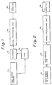
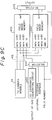
- FIG. 1 is a diagram explaining a conventional high frequency image processing system using a high speed camera.
- This system uses a high speed camera 3a, a scanner 3c, and a picture image processing unit 4a.
- an image on a film 3b picked up by the high speed camera 3a is read by the scanner 3c, and the image is processed by the image processing unit 4.
- FIG. 2 shows another conventional high frequency image processing system.
- a high speed TV camera 3d a high speed VTR 3e, and an image processing unit 4b are used.
- an image caught by the high speed TV camera 3d having a high scanning speed of more than 1/60 seconds/field is once stored in the high speed VTR 3e, then the stored image is output from the VTR 3e, at a normal speed of 1/60 seconds/field, and the output image is processed by the image processing unit 4b.
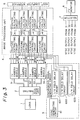
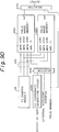
- FIG. 3 is a block diagram showing a high frequency image processing system according to an embodiment of the present invention.
- the system according to the embodiment of the present invention includes four TV camera modules 31 to 34, for an example, each picking up an image at a relatively low scanning frequency of lower than 50 frames/second.
- Each of the TV camera modules 31 to 34 may be a conventional TV camera module having a scanning frequency of 30 frames/second or 60 fields/second.
- each of the TV camera modules 31 to 34 has an electronic shutter, an external synchronization signal input terminal, and an image pickup portion.
- the system shown in Fig. 3 further includes a single lens assembly 1 for focusing light from the image, and a light distributing unit 2 for distributing light from the image through the single lens assembly (1) to the image pickup portions of the respective TV camera modules 31 to 34.
- the system shown in Fig. 3 further includes a synchronization signal generating circuit 6 for generating four synchronization signals.
- the phases of the synchronization signals differ from each other, and the synchronization signals are respectively supplied to the external synchronization signal input terminals of the respective TV camera modules 31 to 34.
- the synchronization signal generating circuit 6 includes a reference signal generating circuit 61 and three 1/4 field delay circuits 621 to 623.
- the output of the synchronization signal generating circuit 61 is connected to the external synchronization signal input terminal of the TV camera module 34, and the 1/4 field delay circuits 621 to 623 are connected in series between the output of the reference signal generating circuit 61 and an external synchronization signal input terminal of the TV camera module 31.
- Each of the 1/4 delay circuits 621 to 623 delays the input signal for 1/4 field, for example.
- the outputs of the 1/4 field delay circuits 621 to 623 are respectively connected to the external synchronization terminals of the TV camera modules 33, 32 and 31, and thus, external synchronization signals having different phases are generated.
- the system shown in Fig. 3 still further includes an image processing unit 4 connected to the outputs of the TV camera modules 31 to 34 and to the outputs of the synchronization signal generating circuit 6.
- the image processing unit 4 processes the signals output from the respective TV camera modules (31 to 34) in response to the synchronization signals from the synchronization signal generating circuit 6.
- the image processing unit 4 includes four feature extracting circuits 411 to 414 respectively connected to the outputs of the TV camera modules 31 to 34. Each of the feature extracting circuits 411 to 414 extracts a predetermined feature from the output signals R, G, and B of the corresponding TV camera module. This predetermined feature is, for example, a portion of the object having a specified color.
- the image processing unit 4 further includes four position calculating circuits 421 to 424 respectively connected to the outputs of the feature extracting circuits 411 to 414 and to the outputs of the synchronization signal generating circuit 6. Each of the position calculating circuits 421 to 424 calculates the position of the extracted feature output from the corresponding feature extracting circuit.
- the electronic shutters in the TV camera modules 31 to 34 are released at different times in response to the synchronization signals, to pick up the image and output four pickup image signals, respectively.
- the image processing unit 44 processes, at different times in response to the synchronization signals, the plurality of pickup image signals respectively output from the plurality of TV camera modules 31 to 34 whereby, after processing the plurality of pickup image signals, the processed pickup image signals as a whole are substantially the same as a signal processed at a relatively high frequency n times higher than the relatively low scanning frequency, where n is equal to the number of TV camera modules 31 to 34.
- the calculated results are sent through a host computer interface 5 to a host computer (not shown).
- a selector 7 is provided to select one of the outputs of the TV camera modules 31 to 34 and the NTSC outputs. The selected output is given to the TV monitor 8.
- each of the TV camera modules 31 to 34 may be a field frequency, and in this case, each of the synchronization signals will be a field synchronization signal.
- each of the TV camera modules 31 to 34 may be a frame frequency, and in this case, each of the synchronization signals will be a frame synchronization signal.
- light from the lens assembly 1 is distributed by the light-distributing unit 2 such as a prism to reach the image pickup surfaces on the respective TV camera modules 31 to 34.
- the synchronization signals having different phases are applied to the respective TV camera modules 31 to 34 and then, in accordance with the synchronization signals, pickup images are output from the TV camera modules.
- the electronic shutters of the TV camera modules 31 to 34 are opened or closed synchronously with the external synchronization signals SYNC.
- a horizontal synchronization signal (HD) or a vertical synchronization signal (VD) for each of the TV camera modules 31 to 34 may be used.
- one moving image processing module is provided to correspond to one TV camera module. Accordingly, if the calculating speed of the moving image processing module is 1/60 seconds/field, image fields of (60 ⁇ the number of TV cameras) can be processed within one second.
- certain features of the image of the object to be picked up are fixed, and positions in the images are calculated. These features are, for example, there are a high brightness, a certain specified color, a certain shape, and so forth.
- To calculate the positions of the extracted features there are known a method of obtaining horizontal and vertical projections and calculating the position of the object by the projections, and a method of calculating the position of the object by the vertical and horizontal coordinates on the picked up image of the extracted pixels.
- the image processing unit 4 is provided with a selector 7 for selecting one of the input signals from the TV camera modules 31 to 34, whereby the image is displayed on the TV monitor so that the lens parameters such as the aperture, zoom, or focus can be easily determined.
- the conventional TV camera modules having a relatively low scanning frequency of 1/60 second/field or 1/30 second/frame, it is possible to input images at a high field frequency or high frame frequency, or at 1/240 second/field or 1/120 second/frame, which is the number of times of the field or frame frequency thereof, this number being equal to the number of TV camera modules 31 to 34, and thus it is possible to output the process result in real time.
- conventional TV camera modules can be used, the system can be constructed at low cost.
- the image can be displayed on conventional TV monitors, an advantage is obtained in that an adjustment of the lens parameters such as the aperture, zoom, or focus is relatively easy.
- the light obtained from the single lens assembly 1 is distributed by the light distributing unit 2, for projecting the light into image picking up elements (CCD) in the four TV camera modules 31 to 34 having electronic shutters, RGB outputs, and NTSC outputs,whereby, the same optical image pictures are always obtained at the above-mentioned image pick-up elements in the four TV camera modules 31 to 34.
- CCD image picking up elements
- each of the half-mirrors passes about 50 % of the incident light, and reflects the remaining about 50 %. Namely, the reflection mirrors as a whole in the figure each reflect 100 % of the incident light. Therefore, by constructing the light distributing unit 2 as shown in Fig. 5, an image from the lens assembly 1 can be input to the four TV camera modules 31 to 34.
- the field synchronization signals SYNC for example, having different phases are generated for an external synchronization of the four TV camera modules 31 to 34, at different timings.
- the SYNC signal which is the basis of the external synchronization signals, is generated, and then the output signal from the SYNC generating circuit 61 is output to the external synchronization signal input terminal of the TV camera module 34.
- the output signal of the SYNC generating circuit 61 is input to the 1/4 field delay circuit 621, to delay the input signal by 1/4 fields, and the output of the 1/4 field delay circuit 621 is input to the external synchronization signal input terminal of the TV camera module 33.
- the output signal of the delay circuit 621 is input to the 1/4 field delay circuit 622, and the output thereof is input to the external synchronization signal input terminal of the TV camera module 32.
- the output signal of the 1/4 field delay circuit 622 is input to a 1/4 field delay circuit 623, and the output thereof is input to the external synchronization signal input terminal of the TV camera module 31.
- the field synchronization signal is generated as an example.
- the above-mentioned SYNC generating circuit 61 is constructed to generate a frame synchronization signal.
- the TV camera modules 31 to 34 output analog image signals (R, G, B and NTSC), in accordance with the respectively given SYNC signals.
- a time chart of these analog image signals is as shown in Figs. 4A to 4D.
- the above-mentioned analog RGB signals are respectively input to the feature extracting circuits 411 to 414.
- Figure 6 shows an example of the feature extracting circuit 411 for extracting a color.
- the other feature extracting circuits 412 to 414 are the same as the circuit shown in Fig. 6.
- the feature extracting circuit 411 includes an A/D converter 415 consisting of three A/D converting circuits 416 to 418, and a color extracting circuit 419.
- the input analog RGB signals are respectively digitized into 8 bits by the three A/D converting circuits 416 to 418, and only a picture element having a specified color is output as a logic "1" (the other portions are logic "0") from the color extracting circuit 419.
- the digital RGB signals from the A/D converting circuits 416 to 418 are converted by a predetermined table (look-up table) given in advance, whereby a pixel of a predetermined color is extracted.
- the selected result of the specified color which is the output of the above-mentioned feature extracting circuit 411, and the SYNC signal, which is the output of the above-mentioned 1/4 field delay circuit 623, are input to the position calculating circuit 421;
- the selected result of the specified color which is the output of the above-mentioned feature extracting circuit 412, and the SYNC signal, which is the output of the above-mentioned 1/4 field delay circuit 622, are input to the position calculating circuit 422;
- the selected result of the specified color which is the output of the above-mentioned feature extracting circuit 413, and the SYNC signal, which is the output of the above-mentioned 1/4 field delay circuit 621, are input to the position calculating circuit 423;
- the selected result of the specified color which is the output of the above-mentioned feature extracting circuit 414, and the SYNC signal, which is the output of the above-mentioned SYNC generating circuit 61
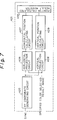
- Figure 7 shows a construction of the position calculating circuit 421; the other position calculating circuits 422 to 424 each have the same construction as the circuit 421.
- the position calculating circuit 421 includes an XY coordinate generating circuit 425, a horizontal projection circuit 426, a horizontal position calculating circuit 427, a vertical projection circuit 428, a vertical position calculating circuit 429, and a position calculating result register 430.
- the SYNC signal which is the output of the 1/4 field delay circuit 623, is input to the XY coordinate generating circuit 425.
- each horizontal line of the above-mentioned SYNC signal is divided by a sampling clock of the above-mentioned A/D converting circuit 415 (see Fig. 6), to thereby generate a X coordinate of the image, and each horizontal line is counted to generate a Y coordinate of the image.
- a horizontal projection circuit 426 the XY coordinates, which are the outputs of the above-mentioned XY coordinate generating circuit 425, and the specified color selected result image, which is the output of the above-mentioned feature extracting circuit 411, are input so that a horizontal projection, which is the total sum of the horizontal lines of the image, is output therefrom.
- a vertical projection circuit 428 In a vertical projection circuit 428, the XY coordinates, which are the outputs of the above-mentioned XY coordinate generating circuit 425, and the specified color selected result image, which is the output of the above-mentioned feature extracting circuit 411, are input so that a vertical projection, which is the total sum of the vertical lines of the image, is output therefrom.
- a horizontal position calculating circuit 427 the position in the X direction of the image of the extracted feature is calculated based on the horizontal projection which is the output of the above-mentioned horizontal projection circuit 426, and the result is stored in a position in the X direction of the position result register 430.
- a vertical position calculating circuit 429 the position in the Y direction of the image of the extracted feature is calculated based on the vertical projection which is the output of the above-mentioned vertical projection circuit 428, and the result is stored in a position in the Y direction of the position result register 430. Also, after the position calculations are finished, calculation completion flags, not shown in the figure, are turned ON.
- the "Colored Object Position Automatic Measuring Apparatus” is used for repeating the processes of receiving red (R), green(G) and blue (B) signals obtained from a color television image, extracting a pixel having a color specified in advance by a host computer, processing the color data to convert same into a binary signal, obtaining projected results in the horizontal and vertical directions of the image for each frame, and determining the position of the specified colored object by the host computer based on the projected results data for each frame, whereby the position of the object having the color is measured automatically and at a video rate.
- the "Video Rate Projection Calculating Circuit” is used for obtaining projection data which is the sum of pixel values in the horizontal direction in a specified region in a given image, in the form of digital video signals, and has two memories, one of which is used for storing a projection result, and the other of which is used for reading out to an external unit. These two memories are used alternatively, and thus the projection results in the horizontal direction can be output at the video rate.
- the vertical projection circuit 428 a technique disclosed in, for example, Japanese Unexamined Patent Publication 63-201789 "Video Rate Projection Calculating Circuit” is used .
- the “Video Rate Projection Calculating Circuit” is used for obtaining projection data which is the sum of pixel values in the vertical direction in a specified region in a given image, in the form of digital video signals, and the circuit is in principle the same as the above-mentioned horizontal projection circuit 421.
- the host computer interface 5 is used for passing the output results from the position calculating circuits 421 to 424 to the not-shown host computer.
- the selector 7 receives the output from a not-shown image synthesising output circuit and the NTSC outputs from the TV camera modules 31 to 34, and selects one thereof each time, to be output to the TV monitor 8.
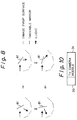
- Figure 8 shows another embodiment in which, as the above-mentioned light distributing unit 2, a movable mirror 81 is used for distributing incident light to the image pickup portions on the TV camera modules, instead of the combination of the half mirrors and total reflection mirrors shown in Fig. 5.
- a movable mirror 81 is used for distributing incident light to the image pickup portions on the TV camera modules, instead of the combination of the half mirrors and total reflection mirrors shown in Fig. 5.
- a movable mirror 81 by rotating the movable mirror 81, light is made incident on the four TV camera modules 31 to 34.
- the movable mirror 81 is rotated synchronously with the external synchronization signal in such a way that, immediately before opening one of the TV camera modules 31 to 34, the light is made incident on the image pickup surface thereof; and while the electronic shutter is open, the movable mirror is kept stationary.
- the movable mirror 81 includes a mirror for reflecting a light received from the lens assembly 1, and a drive unit (not shown in the figure) connected to the outputs of the synchronization signal generating circuit 6, for moving the mirror synchronously with the synchronization signals.
- the light reflected at the mirror is instantly projected, onto the image pickup portion of one of the TV camera modules 31 to 34, before the release of the electronic shutter, and the mirror is kept stationary while the electronic shutter is open.
- the system may include a plurality of lens assemblies respectively provided at the image pickup portions in the TV camera modules 31 to 34.
- the plurality of TV camera modules 31 to 34 are arranged at almost the same position, and the respective lens assemblies are pointed in almost the same direction, to thereby the same image pickup signals from the same image.
- Figure 9A shows a block diagram of a part of the image processing unit 4 operatively connected to the TV camera module 31.
- the other parts of the image processing unit 4 respectively connected to the TV camera modules 32 to 34 are substantially the same as the part shown in Fig. 9A, and are respectively shown in Figs. 9B to 9C.
- the part shown in Fig. 9A includes an A/D converter 415 connected to the output of the TV camera module 31.
- the A/D converter 415 converts analog signals of the picked up image output from the TV camera module 31 into digital signals.
- the part shown in Fig. 9A further includes an XY coordinate generating circuit 431 connected to the output of the reference signal generating circuit 61, for generating XY coordinates of the picked up image based on the reference signal.
- the part shown in Fig. 9A further includes a pair of field image memories 451 and 461, each of the field image memories 451 and 461 having data inputs R, G, and B and an address input.
- the data inputs of the field image memories 451 and 461 are connected to the outputs of the A/D converter 415, and the address inputs of the field image memories 451 and 461 are connected to outputs of a selector 441.
- the pair of field image memories 451 and 461 store the digital signals from the A/D converter 415 by using the synchronization signal as the address signal of the field memories.
- a processor is (not shown in Figs. 9A to 9D) operatively connected to the outputs of the image memories 451 to 454 and 461 to 464, for accessing one of each of the pairs of the field image memories at the same time, to thus read out the stored digital signals and to process the read digital signals, while the outputs of the A/D converters 415 are input into another one of each pair of the field image memories.
- the XY coordinate generating circuits 431 to 434 receive the outputs of 1/4 field delay circuits 621 to 624, and then generate XY coordinates of a field image, for example, in response to each synchronization signal.
- Two sets of field image memories are provided for each of the A/D converters 415, and the image processing is carried out in such a way that, while one of the sets of field image memories 451 and 461 receives the image from the TV camera module 31 by using the XY coordinates as the write accessing address, the other of the sets of field image memories 451 and 461 is accessed by an external accessing address.
- selectors 441 to 444 are provided for changing, at each field, the address given to each of the field image memories 451 to 454 and 461 to 464.
- the selector 441 receives an accessing address from an external world, the output of the XY coordinate generating circuit 431, and the least significant bit of the field number.
- the external accessing address is input to the address input of the field image memory 451
- the output of the XY coordinate generating circuit 431 is input to the address input of the field image memory 461.
- the output of the XY coordinate generating circuit 431 is input to the address input of the field image memory 451, and the external accessing address is input to the address input of the field image memory 461.
- a write enable signal is input to only the field image memory which receives the output of the XY coordinate generating circuit 431.
- RGB digital signals obtained by A/D converting the output of the TV camera module 31, are input to the data inputs of the field image memories 451 and 461, and the selector 471 then operates in such a way that it receives the memory outputs of the field image memories 451 and 461, and the field number, and selects and outputs, to an external unit, the processed image output from the field image memory which is being accessed by the external unit in accordance with the field number.
- one of the sets of the field image memories 451 and 461 receives the image data from the TV camera module 31, the contents of the other set of the field image memories 451 and 461 are read out in accordance with the external accessing address, and the read contents are subjected to an image processing and are output to the external unit.
- a not shown processor can process an image of the one set of field image memories 451 and 461, the image processing can be carried out for continuous fields.
- the description is of an example in which the number of field image memories 451 to 454 and 461 to 464 is twice the number of TV camera modules 31 to 34, but it is of course possible for the number of the field image memories to be the same as the number of TV camera modules 31 to 34.
- This construction also allows a number of fields to be processed, where the number of fields is the same as the number of TV camera modules 31 to 34.
- the TV camera modules 31 to 34 are provided with electronic shutters, but these electronic shutters may be field shutters which carry out shutter operations at each field synchronous with the field synchronization signal, or may be frame shutters which carry out shutter operations at each frame synchronous with the frame synchronization signal.
- an interlace or noninterlace frame scanning method can be used.
- interlace converting circuits must be inserted between the A/D converting circuits 416 to 418 and the color extracting circuit 419.
- a plurality of field/ frame image data from a plurality of conventional TV camera modules with electronic shutters and with external synchronization signals synchronized at different timings are input to process an image at a speed of a number of times the speed of a TV camera modules, this number being equal to the number of TV camera modules.
- an image can be input at a field frequency or a frame frequency which is a number of times of the field frequency or the frame frequency of each TV camera module, this number being equal to the number of TV camera modules, the number of times a processing of the field/frame image is possible, this number being the same as the number of the TV camera modules, and the result can be output in real time.
- the system can be constructed at a low cost, Since the image is displayed by a conventional TV monitor, the adjustment of the lens parameters (aperture, zoom, or focus) of the TV camera modules is made easy, and thus the operability is improved.
Landscapes
- Engineering & Computer Science (AREA)
- Multimedia (AREA)
- Signal Processing (AREA)
- Image Input (AREA)
Applications Claiming Priority (2)
| Application Number | Priority Date | Filing Date | Title |
|---|---|---|---|
| JP236327/90 | 1990-09-06 | ||
| JP2236327A JPH04117776A (ja) | 1990-09-06 | 1990-09-06 | 高画面周波数画像処理方式 |
Publications (2)
| Publication Number | Publication Date |
|---|---|
| EP0474483A2 true EP0474483A2 (fr) | 1992-03-11 |
| EP0474483A3 EP0474483A3 (en) | 1993-05-05 |
Family
ID=16999164
Family Applications (1)
| Application Number | Title | Priority Date | Filing Date |
|---|---|---|---|
| EP19910308111 Withdrawn EP0474483A3 (en) | 1990-09-06 | 1991-09-04 | High speed image pickup system |
Country Status (2)
| Country | Link |
|---|---|
| EP (1) | EP0474483A3 (fr) |
| JP (1) | JPH04117776A (fr) |
Cited By (4)
| Publication number | Priority date | Publication date | Assignee | Title |
|---|---|---|---|---|
| GB2289591A (en) * | 1994-05-06 | 1995-11-22 | Bts Srl | High frame rate video camera |
| EP0701185A1 (fr) * | 1994-09-07 | 1996-03-13 | Imco Electro-Optics Limited | Appareil et méthode pour la prise d'images à grande vitesse |
| EP1453318A1 (fr) * | 2003-02-28 | 2004-09-01 | Shimadzu Corporation | Système photographique à haute vitesse et contrôleur de synchronisation du déclenchement |
| US7084406B2 (en) | 2001-11-16 | 2006-08-01 | Carl Zeiss Nts Gmbh | Detector arrangement and detection method |
Citations (8)
| Publication number | Priority date | Publication date | Assignee | Title |
|---|---|---|---|---|
| JPS59202775A (ja) * | 1983-04-30 | 1984-11-16 | Fuji Electric Co Ltd | 高速ビデオ録画装置 |
| JPS59205877A (ja) * | 1983-05-09 | 1984-11-21 | Toyota Motor Corp | 高速度テレビカメラ装置 |
| JPS63140381A (ja) * | 1986-12-02 | 1988-06-11 | Fujitsu Ltd | ビデオレ−ト投影算出回路 |
| JPS63201789A (ja) * | 1987-02-17 | 1988-08-19 | Fujitsu Ltd | ビデオレ−ト投影算出回路 |
| JPS63314988A (ja) * | 1987-06-18 | 1988-12-22 | Fujitsu Ltd | ビデオレ−ト色抽出装置 |
| JPH01173269A (ja) * | 1987-12-28 | 1989-07-07 | Fujitsu Ltd | 色物体位置自動測定装置 |
| JPH01305781A (ja) * | 1988-06-03 | 1989-12-11 | Mitsubishi Electric Corp | 固体撮像装置 |
| JPH02215293A (ja) * | 1989-02-15 | 1990-08-28 | Matsushita Electric Ind Co Ltd | 高品位テレビジョン表示装置 |
-
1990
- 1990-09-06 JP JP2236327A patent/JPH04117776A/ja active Pending
-
1991
- 1991-09-04 EP EP19910308111 patent/EP0474483A3/en not_active Withdrawn
Patent Citations (8)
| Publication number | Priority date | Publication date | Assignee | Title |
|---|---|---|---|---|
| JPS59202775A (ja) * | 1983-04-30 | 1984-11-16 | Fuji Electric Co Ltd | 高速ビデオ録画装置 |
| JPS59205877A (ja) * | 1983-05-09 | 1984-11-21 | Toyota Motor Corp | 高速度テレビカメラ装置 |
| JPS63140381A (ja) * | 1986-12-02 | 1988-06-11 | Fujitsu Ltd | ビデオレ−ト投影算出回路 |
| JPS63201789A (ja) * | 1987-02-17 | 1988-08-19 | Fujitsu Ltd | ビデオレ−ト投影算出回路 |
| JPS63314988A (ja) * | 1987-06-18 | 1988-12-22 | Fujitsu Ltd | ビデオレ−ト色抽出装置 |
| JPH01173269A (ja) * | 1987-12-28 | 1989-07-07 | Fujitsu Ltd | 色物体位置自動測定装置 |
| JPH01305781A (ja) * | 1988-06-03 | 1989-12-11 | Mitsubishi Electric Corp | 固体撮像装置 |
| JPH02215293A (ja) * | 1989-02-15 | 1990-08-28 | Matsushita Electric Ind Co Ltd | 高品位テレビジョン表示装置 |
Non-Patent Citations (8)
| Title |
|---|
| PATENT ABSTRACTS OF JAPAN vol. 12, no. 399 (P-775)24 October 1988 & JP-A-63 140 381 ( FUJITSU LTD ) 11 June 1988 * |
| PATENT ABSTRACTS OF JAPAN vol. 12, no. 492 (P-804)22 December 1988 & JP-A-63 201 789 ( FUJITSU LTD ) 19 August 1988 * |
| PATENT ABSTRACTS OF JAPAN vol. 13, no. 164 (E-745)19 April 1989 & JP-A-63 314 988 ( FUJITSU LTD ) 22 December 1988 * |
| PATENT ABSTRACTS OF JAPAN vol. 13, no. 448 (P-942)9 October 1989 & JP-A-01 173269 ( FUJITSU LTD ) 7 July 1989 * |
| PATENT ABSTRACTS OF JAPAN vol. 14, no. 105 (E-895)26 February 1990 & JP-A-01 305781 ( MITSUBISHI ELECTRIC CORP. ) 11 December 1989 * |
| PATENT ABSTRACTS OF JAPAN vol. 14, no. 518 (E-1001)14 November 1990 & JP-A-02 215293 ( MATSUSHITA ELECTRIC INDUSTRIAL CO., LTD. ) 28 August 1990 * |
| PATENT ABSTRACTS OF JAPAN vol. 9, no. 65 (E-304)(1788) 26 March 1985 & JP-A-59 202 775 ( FUJI DENKI SEIZO K.K. ) 16 November 1984 * |
| PATENT ABSTRACTS OF JAPAN vol. 9, no. 69 (E-305)(1792) 29 March 1985 & JP-A-59 205 877 ( TOYOTA JIDOSHA K.K. ) 21 November 1984 * |
Cited By (7)
| Publication number | Priority date | Publication date | Assignee | Title |
|---|---|---|---|---|
| GB2289591A (en) * | 1994-05-06 | 1995-11-22 | Bts Srl | High frame rate video camera |
| US5631468A (en) * | 1994-05-06 | 1997-05-20 | B.T.S. Bioingegneria Tecnologia E Sistemi S.R.L. | Telecamera with a high frame frequency and associated manufacturing method |
| GB2289591B (en) * | 1994-05-06 | 1998-10-28 | Bts Srl | Telecamera with a high frame frequency and associated manufacturing method |
| EP0701185A1 (fr) * | 1994-09-07 | 1996-03-13 | Imco Electro-Optics Limited | Appareil et méthode pour la prise d'images à grande vitesse |
| US6157409A (en) * | 1994-09-07 | 2000-12-05 | Imco Electro-Optics Limited | Apparatus and method for high speed imaging |
| US7084406B2 (en) | 2001-11-16 | 2006-08-01 | Carl Zeiss Nts Gmbh | Detector arrangement and detection method |
| EP1453318A1 (fr) * | 2003-02-28 | 2004-09-01 | Shimadzu Corporation | Système photographique à haute vitesse et contrôleur de synchronisation du déclenchement |
Also Published As
| Publication number | Publication date |
|---|---|
| JPH04117776A (ja) | 1992-04-17 |
| EP0474483A3 (en) | 1993-05-05 |
Similar Documents
| Publication | Publication Date | Title |
|---|---|---|
| US6952234B2 (en) | Image pickup apparatus and method for broadening apparent dynamic range of video signal | |
| US7889238B2 (en) | Multicamera system, image pickup apparatus, controller, image pickup control method, image pickup apparatus control method, and image pickup method | |
| WO2005009031A1 (fr) | Appareil de prise de vues et appareil generant un signal de synchronisation | |
| JPH06505853A (ja) | ズーム及びパン効果のためのデジタル画像補間システム | |
| US6876386B1 (en) | Digital camera with downsampling and zoom processing and method of controlling operation of same | |
| JP2000224604A (ja) | 画像処理装置 | |
| EP0474483A2 (fr) | Système de prises d'images à vitesse élevée | |
| JPH06292052A (ja) | 静止画像撮像装置 | |
| KR20050084931A (ko) | 촬상장치 | |
| JPH0870474A (ja) | 立体撮像装置及び立体画像記録再生装置 | |
| JPH06105224A (ja) | ダイナミックレンジ拡大装置 | |
| JP3513200B2 (ja) | 撮像装置 | |
| JPH0772384A (ja) | 立体撮像装置及び立体画像記録再生装置 | |
| JP2984281B2 (ja) | 電子カメラ | |
| EP0989746B1 (fr) | Appareil de prise de vue ayant une fonction de prise de vue à grande vitesse avec circuit de zoom électronique | |
| JP3125903B2 (ja) | 撮像装置 | |
| JP3221004B2 (ja) | ビデオカメラ | |
| JP2868942B2 (ja) | 固体撮像装置 | |
| JP3096756B2 (ja) | 画像変換装置 | |
| JP2618661B2 (ja) | 撮像装置 | |
| EP0993190A2 (fr) | Procédé, appareil et support pour l'enregistrement et reproduction des données d'image | |
| JPH0937128A (ja) | 画像入力装置 | |
| KR100224854B1 (ko) | 영상 처리 방법 | |
| JP2703687B2 (ja) | 電子ズーム方式 | |
| JPH07312717A (ja) | カメラ装置 |
Legal Events
| Date | Code | Title | Description |
|---|---|---|---|
| PUAI | Public reference made under article 153(3) epc to a published international application that has entered the european phase |
Free format text: ORIGINAL CODE: 0009012 |
|
| AK | Designated contracting states |
Kind code of ref document: A2 Designated state(s): DE FR GB |
|
| PUAL | Search report despatched |
Free format text: ORIGINAL CODE: 0009013 |
|
| AK | Designated contracting states |
Kind code of ref document: A3 Designated state(s): DE FR GB |
|
| STAA | Information on the status of an ep patent application or granted ep patent |
Free format text: STATUS: THE APPLICATION IS DEEMED TO BE WITHDRAWN |
|
| 18D | Application deemed to be withdrawn |
Effective date: 19931108 |