EP0472012B1 - Procédé de diffusion de bore dans des disques semi-conducteurs - Google Patents
Procédé de diffusion de bore dans des disques semi-conducteurs Download PDFInfo
- Publication number
- EP0472012B1 EP0472012B1 EP91112736A EP91112736A EP0472012B1 EP 0472012 B1 EP0472012 B1 EP 0472012B1 EP 91112736 A EP91112736 A EP 91112736A EP 91112736 A EP91112736 A EP 91112736A EP 0472012 B1 EP0472012 B1 EP 0472012B1
- Authority
- EP
- European Patent Office
- Prior art keywords
- boron
- temperature
- drive
- source
- diffusion
- Prior art date
- Legal status (The legal status is an assumption and is not a legal conclusion. Google has not performed a legal analysis and makes no representation as to the accuracy of the status listed.)
- Expired - Lifetime
Links
Images

Classifications
-
- H—ELECTRICITY
- H10—SEMICONDUCTOR DEVICES; ELECTRIC SOLID-STATE DEVICES NOT OTHERWISE PROVIDED FOR
- H10P—GENERIC PROCESSES OR APPARATUS FOR THE MANUFACTURE OR TREATMENT OF DEVICES COVERED BY CLASS H10
- H10P32/00—Diffusion of dopants within, into or out of wafers, substrates or parts of devices
- H10P32/10—Diffusion of dopants within, into or out of semiconductor bodies or layers
- H10P32/17—Diffusion of dopants within, into or out of semiconductor bodies or layers characterised by the semiconductor material
- H10P32/171—Diffusion of dopants within, into or out of semiconductor bodies or layers characterised by the semiconductor material being group IV material
-
- H—ELECTRICITY
- H10—SEMICONDUCTOR DEVICES; ELECTRIC SOLID-STATE DEVICES NOT OTHERWISE PROVIDED FOR
- H10P—GENERIC PROCESSES OR APPARATUS FOR THE MANUFACTURE OR TREATMENT OF DEVICES COVERED BY CLASS H10
- H10P32/00—Diffusion of dopants within, into or out of wafers, substrates or parts of devices
- H10P32/10—Diffusion of dopants within, into or out of semiconductor bodies or layers
- H10P32/14—Diffusion of dopants within, into or out of semiconductor bodies or layers within a single semiconductor body or layer in a solid phase; between different semiconductor bodies or layers, both in a solid phase
- H10P32/1408—Diffusion of dopants within, into or out of semiconductor bodies or layers within a single semiconductor body or layer in a solid phase; between different semiconductor bodies or layers, both in a solid phase from or through or into an external applied layer, e.g. photoresist or nitride layers
-
- Y—GENERAL TAGGING OF NEW TECHNOLOGICAL DEVELOPMENTS; GENERAL TAGGING OF CROSS-SECTIONAL TECHNOLOGIES SPANNING OVER SEVERAL SECTIONS OF THE IPC; TECHNICAL SUBJECTS COVERED BY FORMER USPC CROSS-REFERENCE ART COLLECTIONS [XRACs] AND DIGESTS
- Y10—TECHNICAL SUBJECTS COVERED BY FORMER USPC
- Y10S—TECHNICAL SUBJECTS COVERED BY FORMER USPC CROSS-REFERENCE ART COLLECTIONS [XRACs] AND DIGESTS
- Y10S148/00—Metal treatment
- Y10S148/037—Diffusion-deposition
-
- Y—GENERAL TAGGING OF NEW TECHNOLOGICAL DEVELOPMENTS; GENERAL TAGGING OF CROSS-SECTIONAL TECHNOLOGIES SPANNING OVER SEVERAL SECTIONS OF THE IPC; TECHNICAL SUBJECTS COVERED BY FORMER USPC CROSS-REFERENCE ART COLLECTIONS [XRACs] AND DIGESTS
- Y10—TECHNICAL SUBJECTS COVERED BY FORMER USPC
- Y10S—TECHNICAL SUBJECTS COVERED BY FORMER USPC CROSS-REFERENCE ART COLLECTIONS [XRACs] AND DIGESTS
- Y10S438/00—Semiconductor device manufacturing: process
- Y10S438/909—Controlled atmosphere
-
- Y—GENERAL TAGGING OF NEW TECHNOLOGICAL DEVELOPMENTS; GENERAL TAGGING OF CROSS-SECTIONAL TECHNOLOGIES SPANNING OVER SEVERAL SECTIONS OF THE IPC; TECHNICAL SUBJECTS COVERED BY FORMER USPC CROSS-REFERENCE ART COLLECTIONS [XRACs] AND DIGESTS
- Y10—TECHNICAL SUBJECTS COVERED BY FORMER USPC
- Y10S—TECHNICAL SUBJECTS COVERED BY FORMER USPC CROSS-REFERENCE ART COLLECTIONS [XRACs] AND DIGESTS
- Y10S438/00—Semiconductor device manufacturing: process
- Y10S438/914—Doping
- Y10S438/92—Controlling diffusion profile by oxidation
Definitions
- the present invention relates to a method of diffusing boron into semiconductor wafers with oxidation induced stacking faults kept to an absolute minimum.
- BN Boron nitrides
- PPF polyboron films
- a semiconductor wafer is disposed on boats in contact at both sides of the boron source, followed by heating in a diffusion furnace.
- Boron oxide (B 2 O 3 ) generated with heat on the surface of BN, is allowed to fly over the wafer so that glass and diffusion layers of boron, both layers of high concentrations and uniform thicknesses, are formed on the wafer.
- the boron glass layer is then removed by etching, whereas the boron diffusion layer is oxidized again in the furnace at a relatively low temperature of 700°C after which the resulting contamination layer is etched from the boron diffusion layer.
- a boron diffusion step commonly termed a drive-in step is carried out while in heating in the furnace.
- PBF permits direct application or coating over a semiconductor wafer, forming B 2 O 3 and boron glasses of uniform thicknesses with uniform magnitudes of sheet resistance. Moreover, it is by nature easy to handle. PBF has been pondered as a good boron source as taught for instance in Japanese Patent Publication No. 1-60932 and Japanese Patent Laid-open Publication No. 60-92610. This film leaves, despite those advantages, the problem that it involves OSF in a density of more than 100 /cm 2 .
- the present invention seeks to provide a method of diffusing boron into semiconductor wafers which ensures reduction of objectionable OSF to a critical limit of smaller than 20 /cm 2 .
- the boron diffusion method of this invention is suitable particularly for use in semiconductor wafers of greater than 12.5 cm (5 inches) in diameter.
- the invention provides a method of diffusing boron into semiconductor wafers which comprises the following steps in sequence : applying a boron source onto a semiconductor wafer, calcining the source at a temperature from 450 to 800°C and in an oxygen atmosphere of lower than 20% by volume in concentration, performing boron deposition at a temperature from 900 to 1,000°C and in a nitrogen atmosphere, removing a boron glass layer from the semiconductor wafer, and thereafter effecting boron diffusion at a charge temperature substantially equal to or higher than the temperature at the boron deposition step.
- a boron source is applied or coated onto a semiconductor wafer and calcined at a temperature of 450 to 800°C and in an oxygen atmosphere.
- the concentration of oxygen may preferably be not more than 20% by volume.
- a boron deposition step is thereafter performed from 900 to 1,000°C and in a nitrogen atmosphere, removing a boron glass layer formed on the wafer, after which a boron diffusion or drive-in step is finally effected within a specific range of temperatures.
- the drive-in step should be done at a charge temperature set to be substantially equal to or higher than the temperature at the deposition step.
- the charge temperature should range from 890 to 1,000°C, preferably from 900 to 950°C. This temperature if higher than 1,000°C would, though giving sufficient reduction in OSF, adversely affects in incurring a lot of slippage and if lower than 890°C would not be effective in inhibiting or reducing OSF.
- PBF and BN Boron sources eligible for purposes of the invention are PBF and BN of which PBF is more feasible for its handling convenience.
- FIG. 1 is taken to refer to the heat-treating conditions at a drive-in step according to the invention.
- test wafer after being heat-treated in the drive-in step, was HF-treated to remove therefrom an oxidized film, followed by light etching for one minute.
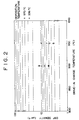
- Counting of OSF/cm 2 was done by means of a 100-magnification, optical microscope with the results shown in FIG. 2.
- the OSF density depends solely upon the temperature at the drive-in step, revealing a decline as the charge temperature rises within the test range from 800 to 1,000°C.
- the OSF density is immune from the dependence on the deposition temperatures at from 936 to 970°C.
- the OSF density is reduced conspicuously to 20 /cm 2 or below.
- the charge temperature at the drive-in step is selected to be substantially equal to or higher than the deposition step so that the OSF density can be held at an acceptable level of not beyond 20 /cm 2 .
- PBF is illustrated as the boron source
- BN may suitably be used with a minimum of OSF densities as in the PBF source.
- the charge temperature at the drive-in step should of course be set within the range specified above.
Landscapes
- Formation Of Insulating Films (AREA)
- Chemical Vapour Deposition (AREA)
Claims (5)
- Procédé de diffusion de bore dans des tranches de semi-conducteurs, comprenant successivement les étapes qui suivent:- l'application d'une source de bore sur une tranche de semi-conducteur ;- la calcination de la source à une température allant de 450 à 800°C, dans une atmosphère d'oxygène ayant une concentration inférieure à 20 % en volume ;- la formation d'un dépôt de bore à une température allant de 900 à 1000°C, dans une atmosphère d'azote ;- l'élimination d'une couche de verre au bore de la tranche ;- et, ensuite, la réalisation d'une diffusion de bore à une température de charge de diffusion supérieure ou sensiblement égale à la température lors de l'étape de dépôt de bore.
- Procédé selon la revendication 1, dans lequel la température de charge de diffusion lors de l'étape de diffusion de bore est comprise dans la plage allant de 890 à 1000°C.
- Procédé selon la revendication 1, dans lequel la source de bore est un film de polybore ou un nitrure de bore.
- Procédé selon la revendication 2, dans lequel la température de charge de diffusion est comprise dans la plage allant de 900 à 950°C.
- Procédé selon la revendication 3, dans lequel la source de bore est un film de polybore.
Applications Claiming Priority (2)
| Application Number | Priority Date | Filing Date | Title |
|---|---|---|---|
| JP220672/90 | 1990-08-22 | ||
| JP2220672A JPH0758698B2 (ja) | 1990-08-22 | 1990-08-22 | 半導体ウエーハヘのボロン拡散方法 |
Publications (3)
| Publication Number | Publication Date |
|---|---|
| EP0472012A2 EP0472012A2 (fr) | 1992-02-26 |
| EP0472012A3 EP0472012A3 (en) | 1992-06-03 |
| EP0472012B1 true EP0472012B1 (fr) | 1996-10-23 |
Family
ID=16754654
Family Applications (1)
| Application Number | Title | Priority Date | Filing Date |
|---|---|---|---|
| EP91112736A Expired - Lifetime EP0472012B1 (fr) | 1990-08-22 | 1991-07-29 | Procédé de diffusion de bore dans des disques semi-conducteurs |
Country Status (4)
| Country | Link |
|---|---|
| US (1) | US5171708A (fr) |
| EP (1) | EP0472012B1 (fr) |
| JP (1) | JPH0758698B2 (fr) |
| DE (1) | DE69122815T2 (fr) |
Families Citing this family (10)
| Publication number | Priority date | Publication date | Assignee | Title |
|---|---|---|---|---|
| JPH0758698B2 (ja) * | 1990-08-22 | 1995-06-21 | 信越半導体株式会社 | 半導体ウエーハヘのボロン拡散方法 |
| US5753530A (en) * | 1992-04-21 | 1998-05-19 | Seiko Instruments, Inc. | Impurity doping method with diffusion source of boron-silicide film |
| EP0709878B1 (fr) * | 1994-10-24 | 1998-04-01 | Naoetsu Electronics Company | Méthode pour la préparation de substrats individuels à partir d'une tranche de silicium semi-conducteur |
| US5674777A (en) * | 1994-10-18 | 1997-10-07 | National Science Council | Method for forming silicon-boron binary compound layer as boron diffusion source in silicon electronic device |
| JPH10154713A (ja) * | 1996-11-22 | 1998-06-09 | Shin Etsu Handotai Co Ltd | シリコンウエーハの熱処理方法およびシリコンウエーハ |
| DE10301244B4 (de) * | 2003-01-15 | 2005-03-17 | Infineon Technologies Ag | Verfahren zum Dotieren von Halbleiterkörpern |
| US8084105B2 (en) * | 2007-05-23 | 2011-12-27 | Applied Materials, Inc. | Method of depositing boron nitride and boron nitride-derived materials |
| US8337950B2 (en) * | 2007-06-19 | 2012-12-25 | Applied Materials, Inc. | Method for depositing boron-rich films for lithographic mask applications |
| RU2475883C1 (ru) * | 2011-09-16 | 2013-02-20 | Федеральное Государственное Унитарное Предприятие "Научно-Производственное Предприятие "Пульсар" | Способ диффузии бора в кремний |
| WO2014123060A1 (fr) * | 2013-02-06 | 2014-08-14 | PVG Solutions株式会社 | Procédé permettant de former une couche de diffusion de bore et procédé permettant de fabriquer une cellule de batterie solaire |
Citations (1)
| Publication number | Priority date | Publication date | Assignee | Title |
|---|---|---|---|---|
| US5171708A (en) * | 1990-08-22 | 1992-12-15 | Shin-Etsu Handotai Co., Ltd. | Method of boron diffusion into semiconductor wafers having reduced stacking faults |
Family Cites Families (7)
| Publication number | Priority date | Publication date | Assignee | Title |
|---|---|---|---|---|
| US3997351A (en) * | 1974-01-07 | 1976-12-14 | Owens-Illinois, Inc. | Glass-ceramic dopant host for vapor phase transport of B2 O3 |
| DE2827330C2 (de) * | 1978-06-22 | 1982-10-21 | Deutsche Itt Industries Gmbh, 7800 Freiburg | Verfahren zur Verminderung des Breitbandrauschens |
| DE3375253D1 (de) * | 1982-09-23 | 1988-02-11 | Allied Corp | Polymeric boron-nitrogen dopant |
| JPS6092610A (ja) * | 1983-10-26 | 1985-05-24 | Rohm Co Ltd | ボロン拡散量の制御方法 |
| JPS6092611A (ja) * | 1983-10-26 | 1985-05-24 | Rohm Co Ltd | 半導体素子の不純物拡散方法 |
| JPS62101026A (ja) * | 1985-10-26 | 1987-05-11 | Shin Etsu Chem Co Ltd | 不純物拡散源 |
| US4791074A (en) * | 1986-08-29 | 1988-12-13 | Kabushiki Kaisha Toshiba | Method of manufacturing a semiconductor apparatus |
-
1990
- 1990-08-22 JP JP2220672A patent/JPH0758698B2/ja not_active Expired - Lifetime
-
1991
- 1991-07-26 US US07/736,546 patent/US5171708A/en not_active Expired - Fee Related
- 1991-07-29 DE DE69122815T patent/DE69122815T2/de not_active Expired - Fee Related
- 1991-07-29 EP EP91112736A patent/EP0472012B1/fr not_active Expired - Lifetime
Patent Citations (1)
| Publication number | Priority date | Publication date | Assignee | Title |
|---|---|---|---|---|
| US5171708A (en) * | 1990-08-22 | 1992-12-15 | Shin-Etsu Handotai Co., Ltd. | Method of boron diffusion into semiconductor wafers having reduced stacking faults |
Non-Patent Citations (2)
| Title |
|---|
| - 159; B.H. JUSTICE ET AL.: 'A Novel Boron Spin-On Dopand' * |
| Solid State Technology/July 1980. N H.Ditrick and M.S. Bae pp69-73 * |
Also Published As
| Publication number | Publication date |
|---|---|
| JPH04102316A (ja) | 1992-04-03 |
| JPH0758698B2 (ja) | 1995-06-21 |
| DE69122815D1 (de) | 1996-11-28 |
| EP0472012A2 (fr) | 1992-02-26 |
| DE69122815T2 (de) | 1997-02-20 |
| EP0472012A3 (en) | 1992-06-03 |
| US5171708A (en) | 1992-12-15 |
Similar Documents
| Publication | Publication Date | Title |
|---|---|---|
| US6391796B1 (en) | Method for heat-treating silicon wafer and silicon wafer | |
| EP0472012B1 (fr) | Procédé de diffusion de bore dans des disques semi-conducteurs | |
| KR20010092733A (ko) | 고유 게터링을 가지는 에피택시얼 실리콘 웨이퍼 및 그제조 방법 | |
| KR19980703246A (ko) | 실리콘 절연체 웨이퍼의 제조를 위한 싱글-에치 스톱 공정 | |
| KR20040013106A (ko) | 표면 거칠기 감소 방법 | |
| US4109030A (en) | Method for thermally oxidizing silicon | |
| JP2742247B2 (ja) | シリコン単結晶基板の製造方法および品質管理方法 | |
| JPH04158514A (ja) | 半導体基板への不純物拡散方法 | |
| Szekeres et al. | Plasma photoresist stripping in a planar reactor | |
| EP0120830B1 (fr) | Matériaux pour substrats semi-conducteurs ayant une capacité de piégeage | |
| Lischner et al. | Observations of the temperature gradient zone melting process for isolating small devices | |
| EP1187189A1 (fr) | Nacelle de silicium a film de protection, procede de fabrication, et plaquette en silicium traitee thermiquement utilisant ladite nacelle | |
| Nagasima et al. | Local Crystallization of Thermal Oxide Film of Silicon | |
| JPS62123098A (ja) | シリコン単結晶の製造方法 | |
| JPH0568099B2 (fr) | ||
| Fang et al. | Defect characteristics and generation mechanism in a bird beak free structure by sidewall masked technique | |
| JP2000286268A (ja) | 半導体シリコンウェーハの製造方法 | |
| JP2601208B2 (ja) | 半導体基体の処理方法 | |
| EP0525455B1 (fr) | Piégeage extrinsèque pour un substrat semi-conducteur | |
| JPS5927529A (ja) | 半導体装置用ウエフアの製造方法 | |
| JPH05206145A (ja) | 半導体装置の製造方法 | |
| JPH05152236A (ja) | 半導体装置の製造方法 | |
| JPH0160932B2 (fr) | ||
| SU686556A1 (ru) | Способ изготовлени @ - @ - @ - @ -структур | |
| Claeys et al. | Impact of high temperature processing on bulk defects in czochralski silicon |
Legal Events
| Date | Code | Title | Description |
|---|---|---|---|
| PUAI | Public reference made under article 153(3) epc to a published international application that has entered the european phase |
Free format text: ORIGINAL CODE: 0009012 |
|
| AK | Designated contracting states |
Kind code of ref document: A2 Designated state(s): DE FR GB |
|
| PUAL | Search report despatched |
Free format text: ORIGINAL CODE: 0009013 |
|
| AK | Designated contracting states |
Kind code of ref document: A3 Designated state(s): DE FR GB |
|
| 17P | Request for examination filed |
Effective date: 19921021 |
|
| 17Q | First examination report despatched |
Effective date: 19950207 |
|
| GRAH | Despatch of communication of intention to grant a patent |
Free format text: ORIGINAL CODE: EPIDOS IGRA |
|
| GRAH | Despatch of communication of intention to grant a patent |
Free format text: ORIGINAL CODE: EPIDOS IGRA |
|
| GRAA | (expected) grant |
Free format text: ORIGINAL CODE: 0009210 |
|
| AK | Designated contracting states |
Kind code of ref document: B1 Designated state(s): DE FR GB |
|
| REF | Corresponds to: |
Ref document number: 69122815 Country of ref document: DE Date of ref document: 19961128 |
|
| ET | Fr: translation filed | ||
| PLBE | No opposition filed within time limit |
Free format text: ORIGINAL CODE: 0009261 |
|
| STAA | Information on the status of an ep patent application or granted ep patent |
Free format text: STATUS: NO OPPOSITION FILED WITHIN TIME LIMIT |
|
| 26N | No opposition filed | ||
| PGFP | Annual fee paid to national office [announced via postgrant information from national office to epo] |
Ref country code: FR Payment date: 19990709 Year of fee payment: 9 |
|
| PGFP | Annual fee paid to national office [announced via postgrant information from national office to epo] |
Ref country code: GB Payment date: 19990728 Year of fee payment: 9 |
|
| PGFP | Annual fee paid to national office [announced via postgrant information from national office to epo] |
Ref country code: DE Payment date: 19990802 Year of fee payment: 9 |
|
| PG25 | Lapsed in a contracting state [announced via postgrant information from national office to epo] |
Ref country code: GB Free format text: LAPSE BECAUSE OF NON-PAYMENT OF DUE FEES Effective date: 20000729 |
|
| GBPC | Gb: european patent ceased through non-payment of renewal fee |
Effective date: 20000729 |
|
| PG25 | Lapsed in a contracting state [announced via postgrant information from national office to epo] |
Ref country code: FR Free format text: LAPSE BECAUSE OF NON-PAYMENT OF DUE FEES Effective date: 20010330 |
|
| REG | Reference to a national code |
Ref country code: FR Ref legal event code: ST |
|
| PG25 | Lapsed in a contracting state [announced via postgrant information from national office to epo] |
Ref country code: DE Free format text: LAPSE BECAUSE OF NON-PAYMENT OF DUE FEES Effective date: 20010501 |