EP0471390A2 - Frequenzteilerschaltung - Google Patents
Frequenzteilerschaltung Download PDFInfo
- Publication number
- EP0471390A2 EP0471390A2 EP91118873A EP91118873A EP0471390A2 EP 0471390 A2 EP0471390 A2 EP 0471390A2 EP 91118873 A EP91118873 A EP 91118873A EP 91118873 A EP91118873 A EP 91118873A EP 0471390 A2 EP0471390 A2 EP 0471390A2
- Authority
- EP
- European Patent Office
- Prior art keywords
- frequency divider
- flip
- circuit
- divider circuit
- output
- Prior art date
- Legal status (The legal status is an assumption and is not a legal conclusion. Google has not performed a legal analysis and makes no representation as to the accuracy of the status listed.)
- Ceased
Links
Images


Classifications
-
- H—ELECTRICITY
- H03—ELECTRONIC CIRCUITRY
- H03K—PULSE TECHNIQUE
- H03K21/00—Details of pulse counters or frequency dividers
- H03K21/38—Starting, stopping or resetting the counter
-
- H—ELECTRICITY
- H03—ELECTRONIC CIRCUITRY
- H03K—PULSE TECHNIQUE
- H03K23/00—Pulse counters comprising counting chains; Frequency dividers comprising counting chains
- H03K23/58—Gating or clocking signals not applied to all stages, i.e. asynchronous counters
Definitions
- the present invention relates to a frequency divider circuit. More particularly, it relates to a resettable frequency divider circuit and an enhancement of its performances.
- Figure 11 shows a construction of a prior art 1/16 frequency divider circuit.
- reference numerals 11B to 14B designate 1/2 frequency divider circuits, respectively, which are constituted by triggered type flip-flops having reset functions.
- Reference numeral 32 designates a buffer circuit for receiving a reset signal.
- Reference characters IN and OUT designate a signal input terminal and a signal output terminal of the resettable frequency divider circuit, respectively.
- Reference characters N1 to N3 designate output terminals of the 1/2 frequency divider circuits 11B to 13B, respectively.
- Reference character N4 designates an output terminal for receiving the reset signal of the buffer circuit 32.
- Reference character RS designates a reset signal input terminal.
- Reference characters D, Q, and R designate input terminals, output terminals, and reset signal input terminals of the 1/2 frequency divider circuits 11B to 14B, respectively.
- This frequency divider circuit will operate as follows.
- Figure 12 shows a relationship between an output signal and a reset input signal of the resettable frequency divider circuit.
- the respective 1/2 frequency divider circuits are constituted by triggered type flip-flops which change their output signals when the input signals are changed to "High”, and the internal nodes of the flip-flops are set to "Low” by the reset signal.
- reference character OUT designates an output signal of the resettable frequency divider circuit.
- Reference character RS designates a reset input signal.
- Reference character T designates a period of the output signal of the frequency divider circuit.
- the output signal (OUT) of the frequency divider circuit becomes "High” at the timing when the reset signal is cancelled, and a frequency division is again started.
- a time period from the cancellation of the reset signal to the rising up of the next output is a period T, and this frequency divider circuit is set to an initial state by the reset signal.
- Figure 14 shows another prior art frequency divider circuit having a division ratio of 1/256 and 1/257.
- reference numeral 33 designates a two-mode frequency divider circuit comprising D flip-flops 33a, 33b, and 33c, which conducts 1/4 and 1/5 frequency division, alternatively.
- Reference numerals 11B to 16B designate 1/2 frequency divider circuits, respectively, which are constituted by T flip-flops.
- Reference numerals 30, 31, 34, and 35 designates OR circuits.
- Reference character IN designates a signal input terminal.
- Reference character MOD designates an input terminal for receiving a frequency division switching signal.
- Reference character OUT designates an output terminal.
- Reference character RS designates a reset signal input terminal.
- this frequency divider circuit at the resetting is as follows.
- the RS signal is "High”
- reset signals are input to the respective D flip-flops 33a to 33c and T flip-flops 11B to 16B, and the operation of the entire circuit is halted.
- Figure 13 shows a construction of a 1/2 frequency divider circuit having a reset function constituted by a field effect transistor.
- reference characters J1 to J13, J21, and J22 designate transistors.
- Reference characters R1 to R4 designate resistors.
- Reference characters I1 to I3 designate constant current sources.
- Reference character V DD designates a power supply terminal.
- Reference character D IN designates an input signal terminal.
- Reference character D R designates a reference voltage signal input terminal.
- Reference character RS designates a reset signal input terminal.
- Reference character OUT designates an output terminal.
- transistors J21 and J22 are newly provided as compared with a usual 1/2 frequency divider circuit having no reset function.
- the transistors J21 and J22 are in OFF states, and the frequency divider circuit conducts a usual operation in a case where the transistors J21 and J22 are not provided, that is, it conducts a 1/2 frequency division operation.
- the reset input signal RS is "High”
- the transistors J21 and J22 are in ON state and the currents flowing through the resistors R2 and R4 become larger than the currents flowing through the resistors R1 and R3, and the 1/2 frequency divider circuit is set to "Low" state.
- a resettable frequency divider circuit comprises means for monitoring at least one of the outputs of flip-flops inside the frequency divider circuit, and means for halting the operation of the prior stage flip-flop which is one stage prior to the flip-flop whose output is monitored when the monitor value is equal to a predetermined value while the reset signal is input. Furthermore, the frequency division operation is restarted at the timing when the cancellation of the reset signal is effected. Therefore, a resettable frequency divider circuit is realized by a simple circuit construction, and there arises no reduction in the operation speed.
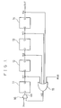
- Figure 1 is a diagram showing a construction of a resettable 1/16 frequency divider circuit according to a first embodiment of the present invention.
- reference numerals 11 to 14 designate 1/2 frequency divider circuits, respectively, which are constituted by flip-flops.
- Reference numeral 15 designates an OR circuit and reference numeral 16 designates an AND circuit.
- Reference characters IN and OUT designate a signal input terminal and a signal output terminal of the resettable frequency divider circuit, respectively.
- Reference characters N1 to N4 designate output terminals of the 1/2 frequency divider circuits 11, 12, 13, and 14.
- Reference character N5 designates an output terminal of the OR circuit 15 and reference character N6 designates an output terminal of the AND circuit 16.
- Reference character RSB designates an input terminal for an inverted signal of the reset signal.
- Reference characters D and Q designate input terminals and output terminals of the 1/2 frequency divider circuits 11 to 14, respectively.
- This resettable frequency divider circuit will operate as follows.
- Figure 2 shows a relationship between the output signal of the resettable frequency divider circuit and the output signals of the respective partial circuits constituted by triggered type flip-flops.
- reference character OUT designates an output signal of the resettable frequency divider circuit and reference characters N1 to N3 designate the output signals of the respective flip-flops.
- Reference character T designates a period of the output signal of the frequency divider circuit. In this frequency divider circuit, it is assumed that the output signals N1, N2, N3, and OUT change when the input signal IN changes from "Low” to "High".
- the outputs of the respective flip-flops 11 to 14 are monitored, and the operation of the first stage flip-flop 11 is halted when the reset signal is input and the values of the monitor become all zero, and accompanying therewith, the operations of the latter stage flip-flops 12 to 14 are halted. Therefore, there is no necessity of providing transistors for providing a reset function inside the flip-flops constituting a frequency divider circuit, whereby a frequency divider circuit which would not arise a reduction in the operation speed is easily realized.
- OR circuit 15 is used for monitoring the internal outputs of the frequency divider circuit, other means may be used therefor.
- Figure 3 shows a resettable 1/16 frequency divider circuit according to a second embodiment of the present invention.
- the same reference numerals as those shown in figure 1 designate the same or corresponding elements.
- Reference numeral 17 designates an AND circuit
- reference numeral 18 designates a NOT circuit
- reference character RS designates a reset signal input terminal.
- the device will operate as follows.
- the signal input to the AND circuit 16 is produced by using the AND circuit 17 and the NOT circuit 18.
- this signal may be produced by using only a NAND circuit 19 as in a third embodiment of the present invention shown in figure 4. Also in this case, a reset operation can be conducted by the same operation as in the second embodiment.
- the operation of the frequency divider circuit is reset when all monitor values have become “Low”, that is, immediately before the output of the frequency divider circuit OUT changes from “Low” to “High” (refer to A in figure 2).
- the operation of the frequency divider circuit is reset when all monitor values become "High”, that is, immediately after the output of the frequency divider circuit OUT changes from "Low” to "High” (refer to B in figure 2).
- an AND circuit 16 is used as means for halting the frequency division operation of the first stage flip-flop, other circuits may be used as in the following.
- Figure 5 shows a resettable 1/16 frequency divider circuit according to a fourth embodiment of the present invention.
- reference numeral 17 designates an AND circuit
- reference numeral 20 designates an OR circuit. While a signal “Low” is input to the terminal RS, the output of the AND circuit 17 is always “Low” and the output N6 of the OR circuit 20 is the input signal IN, and the first stage flip-flop 11 conducts a usual frequency division operation.
- the output of the AND circuit 17 becomes “High” when all output signals N1 to N3 and OUT become “High”
- the output N6 of the OR circuit 20 becomes “High” irrespective of the input signal IN.
- the signal input to the first stage flip-flop 11 becomes “High” and the input signal does not change, whereby the operations of all the flip-flops are halted and are reset.
- an AND circuit 16 is used as a means for halting the input of the first stage flip-flop.
- a switch 21 constituted by such as a transistor may be used as means as in the fifth embodiment of the present invention as shown in figure 6.
- the frequency divider circuit is reset immediately before or immediately after the output of the frequency divider circuit OUT changes from "Low” to "High", the present invention may not be restricted thereto and the reset operation can be realized at an arbitrary period.
- Figure 7 shows a resettable frequency divider circuit according to a sixth embodiment of the present invention.
- the circuit of this sixth embodiment differs from that of the first embodiment shown in figure 1 in that the OR circuit 15 receives the inverted output signal N3 ⁇ as an input signal.
- the method of changing the output OUT for a while after the circuit is reset is especially effective in a case where a high speed frequency divider circuit 36 and a low speed frequency divider circuit 37 are connected in series and they are reset at the same time by the IC circuit 38 as shown in figure 8.
- the low speed frequency divider circuit 37 requires a longer time from the timing when it is reset to the timing when its output changes as compared with the high speed frequency divider circuit 36.
- the reset operation speed of the high speed frequency divider circuit 36 can be easily adjusted with that of the low speed frequency divider circuit 37 by enabling to obtain a change in the output for a while after the high speed frequency divider circuit 36 is reset.
- a signal is used only for resetting the frequency divider circuit.
- the frequency divider circuit is of a type in which the power supply current is controllable by a signal from an external circuit, the external signal can be also used as a reset signal. Such an embodiment will be described.
- Figure 9 shows a resettable frequency divider circuit according to a seventh embodiment of the present invention.
- a two-mode frequency divider circuit of 1/33 and 1/32 modes has a reset function and a current adjusting function.
- reference numeral 10 designates a two-mode frequency divider circuit of 1/4 and 1/5 modes having a reset function.
- Reference numerals 11 to 13 designate 1/2 frequency divider circuits.
- Reference numerals 23, 24, and 25 designate OR circuits.
- Reference numeral J00 designates a transistor for adjusting a circuit current.
- Reference character IN designates a signal input terminal.
- Reference character MOD designates a frequency division number switching input terminal.
- Reference character OUT designates an output terminal.
- Reference character RSB designates an input terminal of an inverted signal of the reset signal.
- Reference character N1 designates an output signal of the two-mode frequency divider circuit 10.
- Reference characters N2 and N3 designate output signals of the 1/2 frequency divider circuits.
- Reference characters N5, N6, and N7 designate output signals of the OR circuits 23, 24, and 25, respectively.
- Reference character N8 designates a source electrode of the transistor J00 and this is connected with the power supply terminals VD of the respective frequency divider circuits 10 to 13.
- Reference characters D, Q, R, VD, and MD designate an input terminal, an output terminal, a reset input terminal, a power supply terminal, and a frequency division number switching terminal, of the frequency divider circuits 10 to 13, respectively.
- This frequency divider circuit will operate as follows.
- the output N7 of the OR circuit 25 When a signal "High” is input to the terminal RSB (that is, a state where the reset signal is “Low”), the output N7 of the OR circuit 25 always becomes “High” and the two-mode frequency divider circuit 10 conducts a usual operation, and a usual current is supplied to the respective frequency divider circuits because the transistor J00 is at ON state. In this case, the two-mode frequency divider circuit 10 conducts a 1/5 frequency division operation when the output N6 is "Low” and it conducts a 1/4 frequency division operation when the output N6 is "High".
- the entire frequency division circuit conducts a 1/(5 + 4 ⁇ 7), that is, 1/33 frequency division operation.
- N6 is always "High” and the two-mode frequency division 10 always conducts a 1/4 frequency division operation.
- the entire frequency division circuit conducts a 1/(4 ⁇ 8), that is, 1/32 frequency division operation.
- the reset function can be provided at the two-mode frequency divider circuit 10 without altering the circuit construction of flip-flops constituting the respective circuits, and there arises no reduction in the operation speed. Furthermore, in this seventh embodiment, the circuit current of the frequency divider circuit is reduced at the reset operation, whereby the power dissipation can be reduced.
- Figure 10 shows an eighth embodiment of the present invention, in which a reset function is provided in a two-mode frequency divider circuit having 1/256 and 1/257 modes.
- reference numeral 10 designates a two-mode frequency divider circuit having 1/4 and 1/5 modes.
- Reference numerals 10a, 10b, and 10c designate D flip-flops.
- Reference numerals 11 to 16 designate 1/2 frequency division circuits constituted by T flip-flops.
- Reference numerals 26, 27, 28, 30, and 31 designate OR circuits.
- Reference numeral 29 designates a NOR circuit.
- the frequency divider circuit can be easily provided with a reset function without changing the circuit construction of flip-flops, and a frequency divider circuit having a high precision reset function, which would not arise a reduction in the operation speed, is realized.
Landscapes
- Stabilization Of Oscillater, Synchronisation, Frequency Synthesizers (AREA)
- Manipulation Of Pulses (AREA)
- Electronic Switches (AREA)
Applications Claiming Priority (2)
| Application Number | Priority Date | Filing Date | Title |
|---|---|---|---|
| JP1148928A JPH0313122A (ja) | 1989-06-12 | 1989-06-12 | 分周回路 |
| JP148928/89 | 1989-06-12 |
Related Parent Applications (2)
| Application Number | Title | Priority Date | Filing Date |
|---|---|---|---|
| EP90302163A Division EP0403047B1 (de) | 1989-06-12 | 1990-02-28 | Frequenzteiler-Schaltung |
| EP90302163.2 Division | 1990-02-28 |
Publications (2)
| Publication Number | Publication Date |
|---|---|
| EP0471390A2 true EP0471390A2 (de) | 1992-02-19 |
| EP0471390A3 EP0471390A3 (en) | 1992-04-08 |
Family
ID=15463800
Family Applications (2)
| Application Number | Title | Priority Date | Filing Date |
|---|---|---|---|
| EP19910118873 Ceased EP0471390A3 (en) | 1989-06-12 | 1990-02-28 | A frequency divider circuit |
| EP90302163A Expired - Lifetime EP0403047B1 (de) | 1989-06-12 | 1990-02-28 | Frequenzteiler-Schaltung |
Family Applications After (1)
| Application Number | Title | Priority Date | Filing Date |
|---|---|---|---|
| EP90302163A Expired - Lifetime EP0403047B1 (de) | 1989-06-12 | 1990-02-28 | Frequenzteiler-Schaltung |
Country Status (4)
| Country | Link |
|---|---|
| US (1) | US5086441A (de) |
| EP (2) | EP0471390A3 (de) |
| JP (1) | JPH0313122A (de) |
| DE (1) | DE69022126T2 (de) |
Cited By (2)
| Publication number | Priority date | Publication date | Assignee | Title |
|---|---|---|---|---|
| DE4214612C2 (de) * | 1992-05-02 | 2001-12-06 | Philips Corp Intellectual Pty | Frequenzteilerschaltung |
| EP1732228A1 (de) * | 2005-06-10 | 2006-12-13 | ATMEL Germany GmbH | Frequenzteilerschaltung mit einem rückgekoppelten Schieberegister |
Families Citing this family (6)
| Publication number | Priority date | Publication date | Assignee | Title |
|---|---|---|---|---|
| JPH05152938A (ja) * | 1991-11-27 | 1993-06-18 | Nec Yamagata Ltd | カウンタ回路 |
| FI100285B (fi) * | 1995-12-11 | 1997-10-31 | Nokia Mobile Phones Ltd | Taajuudenmuodostuspiiri |
| DE19827026C2 (de) * | 1998-06-17 | 2000-05-18 | Siemens Ag | Synchroner Zähler für hohe Taktraten |
| US6072849A (en) * | 1998-08-04 | 2000-06-06 | Vlsi Technology, Inc. | Shift counter device |
| US8218712B1 (en) * | 2010-06-08 | 2012-07-10 | Xilinx, Inc. | Method and apparatus for dividing clock frequencies |
| CN115378424B (zh) * | 2022-10-21 | 2023-02-17 | 上海集成电路研发中心有限公司 | 三分频电路 |
Citations (4)
| Publication number | Priority date | Publication date | Assignee | Title |
|---|---|---|---|---|
| US4150337A (en) * | 1977-11-21 | 1979-04-17 | Rockwell International Corporation | Comparator circuit apparatus |
| US4181862A (en) * | 1976-09-27 | 1980-01-01 | Rca Corporation | High speed resettable dynamic counter |
| JPS5679534A (en) * | 1979-12-01 | 1981-06-30 | Fujitsu Ltd | Initial set system |
| JPS59156028A (ja) * | 1983-02-25 | 1984-09-05 | Iwatsu Electric Co Ltd | クロツク制御型分周回路 |
Family Cites Families (8)
| Publication number | Priority date | Publication date | Assignee | Title |
|---|---|---|---|---|
| US3258696A (en) * | 1962-10-01 | 1966-06-28 | Multiple bistable element shift register | |
| US3639740A (en) * | 1970-07-15 | 1972-02-01 | Collins Radio Co | Ring counter apparatus |
| US3930169A (en) * | 1973-09-27 | 1975-12-30 | Motorola Inc | Cmos odd multiple repetition rate divider circuit |
| JPS5158056A (en) * | 1974-11-18 | 1976-05-21 | Tokyo Shibaura Electric Co | N shinkauntakairo |
| US4334194A (en) * | 1978-12-26 | 1982-06-08 | The United States Of America As Represented By The Secretary Of The Army | Pulse train generator of predetermined pulse rate using feedback shift register |
| JPS5981923A (ja) * | 1982-11-01 | 1984-05-11 | Pioneer Electronic Corp | カウンタ回路 |
| JPS6035400A (ja) * | 1983-08-05 | 1985-02-23 | Sharp Corp | 相補形金属酸化膜半導体を用いた送信装置 |
| US4882505A (en) * | 1986-03-24 | 1989-11-21 | International Business Machines Corporation | Fully synchronous half-frequency clock generator |
-
1989
- 1989-06-12 JP JP1148928A patent/JPH0313122A/ja active Pending
-
1990
- 1990-02-26 US US07/484,854 patent/US5086441A/en not_active Expired - Lifetime
- 1990-02-28 EP EP19910118873 patent/EP0471390A3/en not_active Ceased
- 1990-02-28 EP EP90302163A patent/EP0403047B1/de not_active Expired - Lifetime
- 1990-02-28 DE DE69022126T patent/DE69022126T2/de not_active Expired - Fee Related
Patent Citations (4)
| Publication number | Priority date | Publication date | Assignee | Title |
|---|---|---|---|---|
| US4181862A (en) * | 1976-09-27 | 1980-01-01 | Rca Corporation | High speed resettable dynamic counter |
| US4150337A (en) * | 1977-11-21 | 1979-04-17 | Rockwell International Corporation | Comparator circuit apparatus |
| JPS5679534A (en) * | 1979-12-01 | 1981-06-30 | Fujitsu Ltd | Initial set system |
| JPS59156028A (ja) * | 1983-02-25 | 1984-09-05 | Iwatsu Electric Co Ltd | クロツク制御型分周回路 |
Non-Patent Citations (3)
| Title |
|---|
| FIRST USA-JAPAN COMPUTER CONFERENCE 1972, MONTVALE, N.J US pages 552 - 558; SHUZO YAJIMA ET AL.: 'Power Minimization Problems of Logic Networks' * |
| PATENT ABSTRACTS OF JAPAN vol. 5, no. 145 (E-74)12 September 1981 & JP-A-56 079 534 ( FUJITSU K.K. ) 30 June 1981 * |
| PATENT ABSTRACTS OF JAPAN vol. 9, no. 8 (E-289)(1731) 12 January 1985 & JP-A-59 156 028 ( IWASAKI TSUSHINKI K.K. ) 5 September 1984 * |
Cited By (2)
| Publication number | Priority date | Publication date | Assignee | Title |
|---|---|---|---|---|
| DE4214612C2 (de) * | 1992-05-02 | 2001-12-06 | Philips Corp Intellectual Pty | Frequenzteilerschaltung |
| EP1732228A1 (de) * | 2005-06-10 | 2006-12-13 | ATMEL Germany GmbH | Frequenzteilerschaltung mit einem rückgekoppelten Schieberegister |
Also Published As
| Publication number | Publication date |
|---|---|
| EP0403047A2 (de) | 1990-12-19 |
| EP0403047A3 (de) | 1991-04-17 |
| EP0471390A3 (en) | 1992-04-08 |
| US5086441A (en) | 1992-02-04 |
| DE69022126T2 (de) | 1996-02-15 |
| DE69022126D1 (de) | 1995-10-12 |
| JPH0313122A (ja) | 1991-01-22 |
| EP0403047B1 (de) | 1995-09-06 |
Similar Documents
| Publication | Publication Date | Title |
|---|---|---|
| KR940005506B1 (ko) | 플립플롭회로 | |
| EP0569658B1 (de) | Generator für Signale mit höher Frequenz und nicht-überlappenden Phasen | |
| US4617529A (en) | Ring oscillator with delay element and potential pulling circuit | |
| KR940027316A (ko) | 저전력 모드 및 클럭 증폭기 회로를 가진 집적 회로 | |
| JPS61283092A (ja) | リセツトあるいはセツト付記憶回路を有した半導体集積回路 | |
| EP0471390A2 (de) | Frequenzteilerschaltung | |
| EP0237898A2 (de) | Hockintegrierte Halbleiterschaltung mit Störunterdrückungsschaltung | |
| US4736119A (en) | Dynamic CMOS current surge control | |
| JPS634151B2 (de) | ||
| US5818264A (en) | Dynamic circuit having improved noise immunity and method therefor | |
| US6271735B1 (en) | Oscillator controller with first and second voltage reference | |
| US6069498A (en) | Clock generator for CMOS circuits with dynamic registers | |
| US4398103A (en) | Enabling circuitry for logic circuits | |
| US6060955A (en) | Voltage compensated oscillator and method therefor | |
| JP2563570B2 (ja) | セット・リセット式フリップフロップ回路 | |
| JP2936474B2 (ja) | 半導体集積回路装置 | |
| JPH06132807A (ja) | 出力バッファ能力制御回路 | |
| KR100230408B1 (ko) | 저전력 비교기 회로 및 비교기의 제어방법 | |
| KR100489587B1 (ko) | 시간지연회로 | |
| JP2798510B2 (ja) | 半導体集積回路 | |
| JP2967642B2 (ja) | フリップフロップ回路 | |
| JPH05152905A (ja) | 半導体装置 | |
| JPH0522110A (ja) | 出力回路 | |
| JP2723741B2 (ja) | 半導体集積回路のクロック発生回路 | |
| JPS61173518A (ja) | 信号断検出回路 |
Legal Events
| Date | Code | Title | Description |
|---|---|---|---|
| PUAI | Public reference made under article 153(3) epc to a published international application that has entered the european phase |
Free format text: ORIGINAL CODE: 0009012 |
|
| PUAL | Search report despatched |
Free format text: ORIGINAL CODE: 0009013 |
|
| AC | Divisional application: reference to earlier application |
Ref document number: 403047 Country of ref document: EP |
|
| AK | Designated contracting states |
Kind code of ref document: A2 Designated state(s): DE FR GB |
|
| AK | Designated contracting states |
Kind code of ref document: A3 Designated state(s): DE FR GB |
|
| 17P | Request for examination filed |
Effective date: 19920525 |
|
| 17Q | First examination report despatched |
Effective date: 19931022 |
|
| STAA | Information on the status of an ep patent application or granted ep patent |
Free format text: STATUS: THE APPLICATION HAS BEEN REFUSED |
|
| 18R | Application refused |
Effective date: 19950414 |