FIELD OF THE INVENTION
-
The present invention relates to a frequency divider circuit. More particularly, it relates to a resettable frequency divider circuit and an enhancement of its performances.
BACKGROUND OF THE INVENTION
-
A construction of a prior art resettable frequency divider circuit will be described.
-
Figure 11 shows a construction of a prior art 1/16 frequency divider circuit. In figure 11, reference numerals 11B to 14B designate 1/2 frequency divider circuits, respectively, which are constituted by triggered type flip-flops having reset functions. Reference numeral 32 designates a buffer circuit for receiving a reset signal. Reference characters IN and OUT designate a signal input terminal and a signal output terminal of the resettable frequency divider circuit, respectively. Reference characters N1 to N3 designate output terminals of the 1/2 frequency divider circuits 11B to 13B, respectively. Reference character N4 designates an output terminal for receiving the reset signal of the buffer circuit 32. Reference character RS designates a reset signal input terminal. Reference characters D, Q, and R designate input terminals, output terminals, and reset signal input terminals of the 1/2 frequency divider circuits 11B to 14B, respectively.
-
This frequency divider circuit will operate as follows.
-
When a reset signal is input to the respective 1/2 frequency divider circuits 11B to 14B, the internal signals thereof are compulsorily set to "High" or "Low" state. When the reset signal is cancelled, the respective 1/2 frequency divider circuits operate to divide the input frequency, and the entire circuit conducts a 1/16 frequency division operation.
-
This operation will be described in detail with reference to figure 12.
-
Figure 12 shows a relationship between an output signal and a reset input signal of the resettable frequency divider circuit. Herein, the respective 1/2 frequency divider circuits are constituted by triggered type flip-flops which change their output signals when the input signals are changed to "High", and the internal nodes of the flip-flops are set to "Low" by the reset signal. In figure 12, reference character OUT designates an output signal of the resettable frequency divider circuit. Reference character RS designates a reset input signal. Reference character T designates a period of the output signal of the frequency divider circuit. When a reset signal is input, all internal nodes of the frequency divider circuit are set to "Low" and the output signal (OUT) is set to a state immediately before "High" state. The output signal (OUT) of the frequency divider circuit becomes "High" at the timing when the reset signal is cancelled, and a frequency division is again started. Thus, a time period from the cancellation of the reset signal to the rising up of the next output is a period T, and this frequency divider circuit is set to an initial state by the reset signal.
-
Figure 14 shows another prior art frequency divider circuit having a division ratio of 1/256 and 1/257. In figure 14, reference numeral 33 designates a two-mode frequency divider circuit comprising D flip- flops 33a, 33b, and 33c, which conducts 1/4 and 1/5 frequency division, alternatively. Reference numerals 11B to 16B designate 1/2 frequency divider circuits, respectively, which are constituted by T flip-flops. Reference numerals 30, 31, 34, and 35 designates OR circuits. Reference character IN designates a signal input terminal. Reference character MOD designates an input terminal for receiving a frequency division switching signal. Reference character OUT designates an output terminal. Reference character RS designates a reset signal input terminal.
-
The operation of this frequency divider circuit at the resetting is as follows. When the RS signal is "High", reset signals are input to the respective D flip-flops 33a to 33c and T flip-flops 11B to 16B, and the operation of the entire circuit is halted.
-
In these prior art frequency divider circuits, in order to conduct a reset operation, all flip-flops are required to have reset functions.
-
Figure 13 shows a construction of a 1/2 frequency divider circuit having a reset function constituted by a field effect transistor. In figure 13, reference characters J1 to J13, J21, and J22 designate transistors. Reference characters R1 to R4 designate resistors. Reference characters I1 to I3 designate constant current sources. Reference character VDD designates a power supply terminal. Reference character DIN designates an input signal terminal. Reference character DR designates a reference voltage signal input terminal. Reference character RS designates a reset signal input terminal. Reference character OUT designates an output terminal. In this 1/2 frequency divider circuit, transistors J21 and J22 are newly provided as compared with a usual 1/2 frequency divider circuit having no reset function.
-
The operation of this 1/2 frequency divider circuit will be briefly described.
-
When the reset input signal RS is "Low", the transistors J21 and J22 are in OFF states, and the frequency divider circuit conducts a usual operation in a case where the transistors J21 and J22 are not provided, that is, it conducts a 1/2 frequency division operation. When the reset input signal RS is "High", the transistors J21 and J22 are in ON state and the currents flowing through the resistors R2 and R4 become larger than the currents flowing through the resistors R1 and R3, and the 1/2 frequency divider circuit is set to "Low" state.
-
In the prior art resettable frequency divider circuit, transistors for providing a reset function have to be provided inside the respective 1/2 frequency divider circuits, and this results in a reduction in the operation speed or an increase in the element number for realizing a reset function. Furthermore, since the reset signals have to be given to all 1/2 frequency divider circuits, the buffer circuit 32 is required for supplying reset signals to all flip-flops, and this results in an increase in the power dissipation.
SUMMARY OF THE INVENTION
-
It is an object of the present invention to provide a resettable frequency divider circuit capable of preventing reduction in the operation speed and reducing the power dissipation, and further capable of simplifying the circuit construction.
-
Other objects and advantages of the present invention will become apparent from the detailed description given hereinafter; it should be understood, however, that the detailed description and specific embodiment are given by way of illustration only, since various changes and modifications within the spirit and the scope of the invention will become apparent to those skilled in the art from this detailed description.
-
According to an aspect of the present invention, a resettable frequency divider circuit comprises means for monitoring at least one of the outputs of flip-flops inside the frequency divider circuit, and means for halting the operation of the prior stage flip-flop which is one stage prior to the flip-flop whose output is monitored when the monitor value is equal to a predetermined value while the reset signal is input. Furthermore, the frequency division operation is restarted at the timing when the cancellation of the reset signal is effected. Therefore, a resettable frequency divider circuit is realized by a simple circuit construction, and there arises no reduction in the operation speed.
BRIEF DESCRIPTION OF THE DRAWINGS
-
- Figure 1 is a diagram showing a resettable frequency divider circuit according to a first embodiment of the present invention;
- Figure 2 is a diagram showing the output of the resettable frequency divider circuit of figure 1 and the output waveforms of the respective flip-flops thereof;
- Figure 3 is a diagram showing a resettable frequency divider circuit according to a second embodiment of the present invention;
- Figure 4 is a diagram showing a resettable frequency divider circuit according to a third embodiment of the present invention;
- Figure 5 is a diagram showing a resettable frequency divider circuit according to a fourth embodiment of the present invention;
- Figure 6 is a diagram showing a resettable frequency divider circuit according to a fifth embodiment of the present invention;
- Figure 7 is a diagram showing a resettable frequency divider circuit according to a sixth embodiment of the present invention;
- Figure 8 is a diagram showing a circuit for explaining the effect of the resettable frequency divider circuit of figure 7;
- Figure 9 is a diagram showing a resettable frequency divider circuit according to a seventh embodiment of the present invention;
- Figure 10 is a diagram showing a resettable frequency divider circuit according to an eighth embodiment of the present invention;
- Figure 11 is a diagram showing a prior art resettable frequency divider circuit;
- Figure 12 is a diagram showing a relationship between a reset input signal and an output of the resettable frequency divider circuit according to the prior art;
- Figure 13 is a diagram showing a 1/2 frequency divider circuit having a reset function constituted by field effect transistors; and
- Figure 14 is a diagram showing a resettable frequency divider circuit according to another prior art.
DETAILED DESCRIPTION OF THE PREFERRED EMBODIMENTS
-
An embodiment of the present invention will be described in detail with reference to the drawings.
-
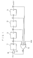
Figure 1 is a diagram showing a construction of a resettable 1/16 frequency divider circuit according to a first embodiment of the present invention. In figure 1, reference numerals 11 to 14 designate 1/2 frequency divider circuits, respectively, which are constituted by flip-flops. Reference numeral 15 designates an OR circuit and reference numeral 16 designates an AND circuit. Reference characters IN and OUT designate a signal input terminal and a signal output terminal of the resettable frequency divider circuit, respectively. Reference characters N1 to N4 designate output terminals of the 1/2 frequency divider circuits 11, 12, 13, and 14. Reference character N5 designates an output terminal of the OR circuit 15 and reference character N6 designates an output terminal of the AND circuit 16. Reference character RSB designates an input terminal for an inverted signal of the reset signal. Reference characters D and Q designate input terminals and output terminals of the 1/2 frequency divider circuits 11 to 14, respectively.
-
This resettable frequency divider circuit will operate as follows.
-
First of all, while a signal "High" is input to the terminal RSB (that is, a state where the reset signal is "Low"), the output N5 of the OR circuit 15 is always "High" and the output N6 of the AND circuit 16 which is an input signal of the first stage flip-flop 11 becomes the input signal IN, and a usual frequency division operation is conducted. In this case, the respective flip-flops 11 to 14 conduct a 1/2 frequency division operation, and the entire circuit conducts a 1/16 frequency division operation.
-
Next, while a signal "Low" is input to the terminal RSB (that is, a state where the reset signal is "High"), the output N5 of the OR circuit 15 becomes "Low" when all the signals N1 to N3 and OUT are "Low", and the output N6 of the AND circuit 16 becomes "Low" irrespective of the input signal IN. Thus, the signal input to the first stage flip-flop 11 becomes "Low". Herein, while the input of the respective flip-flops 11 to 14 do not change, the outputs thereof do not change. That is, while N6 does not change from the "Low" state, the output N1 of the flip-flop 11 does not change. While N1 does not change, the output N2 of the flip-flop 12 does not change. In this way, when the prior stage flip-flop is halted, the latter stage flip-flop is halted, and as a result, the operation of all the flip-flops are halted. Then, these flip-flops 11 to 14 are at "Low" state.
-
When a signal "High" is input to the terminal RSB in this state (that is, a state where the reset signal is "low"), the output N5 of the OR circuit 15 becomes "High" and the input signal IN becomes the output N6 of the AND circuit 16, and the usual frequency division is restarted.
-
This operation will be described with reference to figure 2. Figure 2 shows a relationship between the output signal of the resettable frequency divider circuit and the output signals of the respective partial circuits constituted by triggered type flip-flops. In figure 2, reference character OUT designates an output signal of the resettable frequency divider circuit and reference characters N1 to N3 designate the output signals of the respective flip-flops. Reference character T designates a period of the output signal of the frequency divider circuit. In this frequency divider circuit, it is assumed that the output signals N1, N2, N3, and OUT change when the input signal IN changes from "Low" to "High".
-
In this case, the relationships between the respective signals are as shown in figure 2, and the output signals of all the flip-flops become "Low" immediately before the output of the frequency divider circuit OUT changes to "High" from "Low" (refer to A in figure 2). When the output N5 of the OR circuit 15 becomes "Low", the output N6 of the AND circuit 16 becomes "Low" irrespective of the input signal IN, and the operation of the first stage flip-flop 11 is halted and its output N1 is held at "Low" state. When the output N1 of the first stage flip-flop 11 is halted, the latter stage flip-flops 12 to 14 are also halted, and the entire frequency divider circuit holds the state immediately before its output OUT changes to "High". When a signal "High" is input to the terminal RSB in this state, the output N5 becomes "High" and the input signal IN appears at N6, and a frequency division operation is started. Since all the flip-flops 11 to 14 are set at "Low" immediately before the frequency division operation is started, the output rises at the timing when the signal of the terminal RSB becomes "High", and the same function as that of the prior art resettable frequency divider circuit is realized.
-
In this embodiment, the outputs of the respective flip-flops 11 to 14 are monitored, and the operation of the first stage flip-flop 11 is halted when the reset signal is input and the values of the monitor become all zero, and accompanying therewith, the operations of the latter stage flip-flops 12 to 14 are halted. Therefore, there is no necessity of providing transistors for providing a reset function inside the flip-flops constituting a frequency divider circuit, whereby a frequency divider circuit which would not arise a reduction in the operation speed is easily realized.
-
While in the above-illustrated embodiment an OR circuit 15 is used for monitoring the internal outputs of the frequency divider circuit, other means may be used therefor.
-
Figure 3 shows a resettable 1/16 frequency divider circuit according to a second embodiment of the present invention. In figure 3, the same reference numerals as those shown in figure 1 designate the same or corresponding elements. Reference numeral 17 designates an AND circuit, reference numeral 18 designates a NOT circuit, and reference character RS designates a reset signal input terminal.
-
The device will operate as follows.
-
While a signal "Low" is input to the terminal RS, the output of the AND circuit 17 is always "Low", and it is inverted by the NOT circuit 18 and the signal input to the AND circuit 16 is always "High". Thus, the input signal IN appears at N6 and the first stage flip-flop 11 conducts a usual frequency division operation.
-
Next, when a signal "High" is input to the terminal RS, the output of the AND circuit 17 becomes "High" when all the signals N1 to N3 and OUT become "High" (refer to B in figure 2) and it is inverted by the NOT circuit 18, and the signal input to the AND circuit 16 is always "Low". Thus, the output N6 of the AND circuit 16 always becomes "Low" irrespective of the input signal IN. That is, because the signal input to the first stage flip-flop 11 does not change, operations of all flip-flops are halted.
-
In the above-described second embodiment, the signal input to the AND circuit 16 is produced by using the AND circuit 17 and the NOT circuit 18. However, this signal may be produced by using only a NAND circuit 19 as in a third embodiment of the present invention shown in figure 4. Also in this case, a reset operation can be conducted by the same operation as in the second embodiment.
-
In the above-described first embodiment, the operation of the frequency divider circuit is reset when all monitor values have become "Low", that is, immediately before the output of the frequency divider circuit OUT changes from "Low" to "High" (refer to A in figure 2). In this second and third embodiments, the operation of the frequency divider circuit is reset when all monitor values become "High", that is, immediately after the output of the frequency divider circuit OUT changes from "Low" to "High" (refer to B in figure 2).
-
While in the first to third embodiments an AND circuit 16 is used as means for halting the frequency division operation of the first stage flip-flop, other circuits may be used as in the following.
-
Figure 5 shows a resettable 1/16 frequency divider circuit according to a fourth embodiment of the present invention. In figure 5, reference numeral 17 designates an AND circuit and reference numeral 20 designates an OR circuit. While a signal "Low" is input to the terminal RS, the output of the AND circuit 17 is always "Low" and the output N6 of the OR circuit 20 is the input signal IN, and the first stage flip-flop 11 conducts a usual frequency division operation. When a signal "High" is input to the terminal RS, the output of the AND circuit 17 becomes "High" when all output signals N1 to N3 and OUT become "High", and the output N6 of the OR circuit 20 becomes "High" irrespective of the input signal IN. Thus, the signal input to the first stage flip-flop 11 becomes "High" and the input signal does not change, whereby the operations of all the flip-flops are halted and are reset.
-
In the above-described first to third embodiments, an AND circuit 16 is used as a means for halting the input of the first stage flip-flop. However, a switch 21 constituted by such as a transistor may be used as means as in the fifth embodiment of the present invention as shown in figure 6.
-
In the above-described first to fifth embodiments, the frequency divider circuit is reset immediately before or immediately after the output of the frequency divider circuit OUT changes from "Low" to "High", the present invention may not be restricted thereto and the reset operation can be realized at an arbitrary period.
-
Figure 7 shows a resettable frequency divider circuit according to a sixth embodiment of the present invention. The circuit of this sixth embodiment differs from that of the first embodiment shown in figure 1 in that the
OR circuit 15 receives the inverted output signal
as an input signal.
-
When a signal "Low" is input to the terminal RSB and all the output signals N1, N2,
, and OUT become "Low", the output of the
OR circuit 15 becomes "Low" and the output N6 of the AND
circuit 16 becomes "Low" irrespective of the input signal IN, and all the flip-flops are reset. Herein, the period when the output signals N1, N2,
, and OUT become "Low" is the period C of figure 2 when the output signals N1, N2, and OUT are "Low" and N3 is "High". In this case, the OUT is reset for a while after it changes to "High".
-
The method of changing the output OUT for a while after the circuit is reset is especially effective in a case where a high speed frequency divider circuit 36 and a low speed frequency divider circuit 37 are connected in series and they are reset at the same time by the IC circuit 38 as shown in figure 8. In this case, the low speed frequency divider circuit 37 requires a longer time from the timing when it is reset to the timing when its output changes as compared with the high speed frequency divider circuit 36. However, the reset operation speed of the high speed frequency divider circuit 36 can be easily adjusted with that of the low speed frequency divider circuit 37 by enabling to obtain a change in the output for a while after the high speed frequency divider circuit 36 is reset.
-
Furthermore, while in the above-described first to sixth embodiments the operation of the prior stage flip-flop is halted by halting its input signal, a reset function may be provided only at the prior stage flip-flop. Also in this case, the similar operation as that of the above-described embodiment can be obtained.
-
Furthermore, in the above-described embodiments, a signal is used only for resetting the frequency divider circuit. However, if the frequency divider circuit is of a type in which the power supply current is controllable by a signal from an external circuit, the external signal can be also used as a reset signal. Such an embodiment will be described.
-
Figure 9 shows a resettable frequency divider circuit according to a seventh embodiment of the present invention. In this resettable frequency divider circuit, a two-mode frequency divider circuit of 1/33 and 1/32 modes has a reset function and a current adjusting function. In figure 9, reference numeral 10 designates a two-mode frequency divider circuit of 1/4 and 1/5 modes having a reset function. Reference numerals 11 to 13 designate 1/2 frequency divider circuits. Reference numerals 23, 24, and 25 designate OR circuits. Reference numeral J00 designates a transistor for adjusting a circuit current. Reference character IN designates a signal input terminal. Reference character MOD designates a frequency division number switching input terminal. Reference character OUT designates an output terminal. Reference character RSB designates an input terminal of an inverted signal of the reset signal. Reference character N1 designates an output signal of the two-mode frequency divider circuit 10. Reference characters N2 and N3 designate output signals of the 1/2 frequency divider circuits. Reference characters N5, N6, and N7 designate output signals of the OR circuits 23, 24, and 25, respectively. Reference character N8 designates a source electrode of the transistor J00 and this is connected with the power supply terminals VD of the respective frequency divider circuits 10 to 13. Reference characters D, Q, R, VD, and MD designate an input terminal, an output terminal, a reset input terminal, a power supply terminal, and a frequency division number switching terminal, of the frequency divider circuits 10 to 13, respectively.
-
This frequency divider circuit will operate as follows.
-
When a signal "High" is input to the terminal RSB (that is, a state where the reset signal is "Low"), the output N7 of the OR circuit 25 always becomes "High" and the two-mode frequency divider circuit 10 conducts a usual operation, and a usual current is supplied to the respective frequency divider circuits because the transistor J00 is at ON state. In this case, the two-mode frequency divider circuit 10 conducts a 1/5 frequency division operation when the output N6 is "Low" and it conducts a 1/4 frequency division operation when the output N6 is "High". That is, only when the MOD is "Low" and N2 to N3 and OUT are all "Low", the output N6 of the OR circuit 24 becomes "Low", and the two-mode frequency division circuit 10 conducts a 1/5 frequency division operation. Thus, the entire frequency division circuit conducts a 1/(5 + 4 × 7), that is, 1/33 frequency division operation. On the other hand, when the MOD is "high", N6 is always "High" and the two-mode frequency division 10 always conducts a 1/4 frequency division operation. Thus, the entire frequency division circuit conducts a 1/(4 × 8), that is, 1/32 frequency division operation.
-
Next, when the RSB signal is "Low" (that is, the reset signal is "High"), the output N7 of the OR circuit 25 becomes "Low" when N5 is "Low", that is, N2, N3, and OUT are all "Low", and a signal "Low" is input to the reset terminal R of the two-mode frequency division circuit 10, whereby the operation of the two-mode frequency division circuit 10 is halted. Since the respective circuits 10 to 13 are frequency divider circuits, their outputs do not change while their inputs do not change. Therefore, when the operation of the prior stage frequency divider circuit is halted, the latter stage frequency divider circuit will be halted. As a result, the operations of all circuits are halted.
-
Furthermore, when the output signal N7 becomes "Low", the circuit current of the frequency divider circuit is lowered due to the transistor J00 provided between the power supply VDD and the frequency divider circuit. Then, the states of the respective circuits 10 to 13 are "Low". When the RSB signal changes to "High" (that is, a state where the reset signal is "Low"), the output N7 of the OR circuit 25 changes to "High", and the reset signal of the two-mode frequency divider circuit 10 is cancelled and a usual frequency division operation is started.
-
In the above-described seventh embodiment, similarly as in the above-described embodiments, the reset function can be provided at the two-mode frequency divider circuit 10 without altering the circuit construction of flip-flops constituting the respective circuits, and there arises no reduction in the operation speed. Furthermore, in this seventh embodiment, the circuit current of the frequency divider circuit is reduced at the reset operation, whereby the power dissipation can be reduced.
-
Figure 10 shows an eighth embodiment of the present invention, in which a reset function is provided in a two-mode frequency divider circuit having 1/256 and 1/257 modes. In figure 10, reference numeral 10 designates a two-mode frequency divider circuit having 1/4 and 1/5 modes. Reference numerals 10a, 10b, and 10c designate D flip-flops. Reference numerals 11 to 16 designate 1/2 frequency division circuits constituted by T flip-flops. Reference numerals 26, 27, 28, 30, and 31 designate OR circuits. Reference numeral 29 designates a NOR circuit.
-
The operation of this frequency divider circuit at the reset operation will be described. When a signal "Low" is input to the terminal RSB (that is, the reset signal is "High"), the output of the NOR circuit 29 becomes "High" when all the outputs of the T flip-flops 11 to 16 are "Low", and the output of the OR circuit 30 which is at the prior stage of the two-mode frequency divider circuit 10 always becomes "High", and a signal "High" is always input to the input data terminal D of the D flip-flop 10a, and the operation of the first stage two-mode frequency divider circuit 10 is halted. As a result, the operation of the entire circuit is halted.
-
In this eighth embodiment, there is provided a logic circuit in which the outputs of the respective flip-flops are monitored and a signal "High" is always input to the data input at the first stage of the D flip-flop when all the outputs which are monitored are "Low", and a reset operation is conducted by the first stage flip-flop being halted in such case. Therefore, the frequency divider circuit can be easily provided with a reset function without changing the circuit construction of flip-flops, and a frequency divider circuit having a high precision reset function, which would not arise a reduction in the operation speed, is realized.
-
As is evident from the foregoing description, according to the present invention, there are provided a function of monitoring at least one of the outputs of the flip-flops inside the entire frequency divider circuit and a function of halting the operation of the prior stage flip-flop which is one stage prior to the flip-flops whose output are monitored. Therefore, a resettable frequency divider circuit is realized by a simple circuit construction, and there arises no lowering in the operation speed because an alteration of circuit for providing a reset function has no influence on a flip-flop constituting a frequency divider circuit, and furthermore, a resettable frequency divider circuit can be easily realized from a frequency divider circuit having no reset function.
-
In a construction where the operation of the prior stage flip-flop which is one stage prior to the flip-flop whose output is monitored is halted when the monitor value is equal to a predetermined value and the monitor value is set at the predetermined value immediately before the frequency operation is restarted, an effect of reducing the power dissipation can be further obtained because the circuit current of the frequency division circuit can be lowered.