EP0470570B1 - Method and apparatus for byte order switching in a computer - Google Patents
Method and apparatus for byte order switching in a computer Download PDFInfo
- Publication number
- EP0470570B1 EP0470570B1 EP91113177A EP91113177A EP0470570B1 EP 0470570 B1 EP0470570 B1 EP 0470570B1 EP 91113177 A EP91113177 A EP 91113177A EP 91113177 A EP91113177 A EP 91113177A EP 0470570 B1 EP0470570 B1 EP 0470570B1
- Authority
- EP
- European Patent Office
- Prior art keywords
- byte
- program
- byte order
- bits
- machine
- Prior art date
- Legal status (The legal status is an assumption and is not a legal conclusion. Google has not performed a legal analysis and makes no representation as to the accuracy of the status listed.)
- Expired - Lifetime
Links
Images
Classifications
-
- G—PHYSICS
- G06—COMPUTING; CALCULATING OR COUNTING
- G06F—ELECTRIC DIGITAL DATA PROCESSING
- G06F7/00—Methods or arrangements for processing data by operating upon the order or content of the data handled
- G06F7/76—Arrangements for rearranging, permuting or selecting data according to predetermined rules, independently of the content of the data
- G06F7/768—Data position reversal, e.g. bit reversal, byte swapping
-
- G—PHYSICS
- G06—COMPUTING; CALCULATING OR COUNTING
- G06F—ELECTRIC DIGITAL DATA PROCESSING
- G06F9/00—Arrangements for program control, e.g. control units
- G06F9/06—Arrangements for program control, e.g. control units using stored programs, i.e. using an internal store of processing equipment to receive or retain programs
- G06F9/30—Arrangements for executing machine instructions, e.g. instruction decode
- G06F9/34—Addressing or accessing the instruction operand or the result ; Formation of operand address; Addressing modes
Definitions
- This invention is in the field of digital computers.
- a method and apparatus for enabling a computer to run programs which utilize either of at least two different byte orders is disclosed.
- the present invention in one of its embodiments, corrects the known disadvantages of the prior art by providing a software module, compatible with most microprocessors, which allows a BE program to run on a LE machine and vice versa.
- the module is part of the operating system software and utilizes the fact that for computer words containing four bytes of data, XORing the low two bits of the address of one word with binary 3 results in addressing the desired byte for a machine of opposite byte order.
- a software and hardware implementation of the present invention are possible. Although a software implementation requires no additional or special hardware, it does run slower than a hard-wired apparatus to perform the same function. Therefore, in some circumstances, a hardware implementation of the present invention would be desirable.
- a bit in one register is set or unset to indicate big or little endianess. The bit indicates that the endianess of certain part-word instructions must be changed.
- the present invention allows a single computer to run programs intended for either BE or LE order.
- a simple technique called endian switching allows one computer to mimic a computer of different byte order with a minor performance overhead.
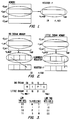
- BE and LE machines The difference between BE and LE machines is shown herein by the interpretation of the lower two bits of the address when using byte memory operations.
- a LE machine selects the 8 bits that include the least significant bit (“LSB”) when the address has 00 as the lower two bits.
- a BE machine selects the 8 bits that contains the most significant bits (“MSB”) when using the same address bits. In some BE machines, the byte selected would include the sign bit for the data.
- Figure 2 shows a load byte operation for both a BE and LE machine.
- the word that contains the desired byte is extracted from memory using only the word address and is placed in an alignment register.
- a reset-time set_endian flag which is initialized during power-up routines, is used to indicate what type of machine is being used and which 8 bits are to be placed in the LSB position in the register.
- the BE memory places the sign and most significant bit into the lowest byte address and the LE memory places the least significant bit in the same place.
- Figure 3 illustrates the principle that by using the two low order address bits to number the bytes starting from either the least significant bit ("LSB”) or most significant bit (“MSB”), either a BE or LE machine can be created.
- the byte addressed by the low two bits 00 for the BE machine contains an 'M' and the two high bits 11 address a byte containing an 'S'.
- the LE machine the situation is exactly reversed - the byte addressed by 00 contains an 'S' and the byte addressed by 11 contains an 'M'.
- exclusive OR-ing 'XORing'
- the byte address used by either machine with "11" binary 3 results in the correct byte address to access the same data using the opposite data ordering convention.
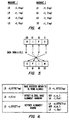
- Figure 4 further shows how the two types of machine are really quite similar in that merely changing the offset of a given address can make a given machine act like a machine of a different byte order. It should also be noted that the offsets for different machines are, in this example, mirror images of each other.
- Figure 5 shows a string of characters in a file 15 and how those characters are mapped into a word by a BE machine 20 and a LE machine 25. As the figure illustrates, it is the combination of how the processor extracts bytes from a word and how the I/O system assembles and disassembles words that establish whether a machine is BE or LE.
- the first convention the interpretation of the low address bits, is implemented in software as part of the computer in a preferred embodiment of the present invention and relies on the observation of that byte addresses in one byte order can be made to simulate those of the other byte order by XORing the two low order bits of the first byte order with binary three.
- the software to perform this task functions at or after the program's compilation time.
- the computer containing the present invention for inverting the byte order can read the program to be loaded and adjust each partial word memory reference to account for the different convention of how bytes are packed in a word.
- the system notes that the bit indicating a different "endianess" has been turned on. Instructions which access parts of words are not altered. Instead, the 32 bit address bus has a branch pathway. 30 bits of the address are placed in a load aligner register. The remaining two bits are XORed with binary 3 to obtain the correct byte address. The 30-bits and 2-bits are then recombined in the load aligner. This method does not degrade the system's performance as the program is operating exactly as it would have had the reset time flag been set to the indicated byte order. These operations will only occur if the system is both in user mode and the reverse endian bit is on. The instructions affected include the load and store instructions.
- the second convention, conversion of words into and from byte streams in the I/O system, is also accomplished in software in the preferred embodiment.
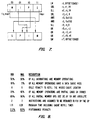
- Word swapping is the operation of exchanging the two outer bytes and the two inner bytes (switch bytes 0 and 3 and switch bytes 1 and 2). Word swapping and the code necessary to implement it are shown in Figure 7.
- the operating system must be able both to emulate the opposite byte order and to emulate the system assumptions of the program being run. This can require both a compatible system call vector and, possibly, conversion of the data structure being passed. Every binary load module has its byte order encoded at the beginning of the module. This informs the operating system of the actions needed to emulate the program's system assumptions.
- the operating system can identify a binary number of a different "endianess" and select a separate vector. If there are no or only a few overlaps in the assigned system calls, the entry to the opposite endian system call can change the data structure being passed (if any) and branch into the original system call.
- Programs are stored as files in a byte order that assumes that the input/output mechanism converts the character data into words. Therefore, the organization of the program must be changed before the program is executed. As described, this is relatively easy, as every instruction in the load module and every initialed data word will be swapped. One reason the bytes are switched is because the network interface is byte oriented and intrinsically swaps words when moving from BE to LE and back. Compensation is thus needed.
- Figure 8 shows an estimate of the impact of simulating the opposite byte order in software.
- the hardware extension incurs no performance cost during the computational part of the program as the program runs exactly as it would on a machine of the other byte order.
- the range of the software penalty is 2-8.8%. Converting the input/output buffers will also cause a certain loss of performance. This is on the order of 11.7% longer to read and word swap a file than to just read the file.
Landscapes
- Engineering & Computer Science (AREA)
- Theoretical Computer Science (AREA)
- Software Systems (AREA)
- Physics & Mathematics (AREA)
- General Engineering & Computer Science (AREA)
- General Physics & Mathematics (AREA)
- Executing Machine-Instructions (AREA)
- Memory System (AREA)
- Stored Programmes (AREA)
Applications Claiming Priority (2)
| Application Number | Priority Date | Filing Date | Title |
|---|---|---|---|
| US56492390A | 1990-08-09 | 1990-08-09 | |
| US564923 | 1990-08-09 |
Publications (3)
| Publication Number | Publication Date |
|---|---|
| EP0470570A2 EP0470570A2 (en) | 1992-02-12 |
| EP0470570A3 EP0470570A3 (en) | 1993-06-30 |
| EP0470570B1 true EP0470570B1 (en) | 1997-01-29 |
Family
ID=24256454
Family Applications (1)
| Application Number | Title | Priority Date | Filing Date |
|---|---|---|---|
| EP91113177A Expired - Lifetime EP0470570B1 (en) | 1990-08-09 | 1991-08-06 | Method and apparatus for byte order switching in a computer |
Country Status (4)
| Country | Link |
|---|---|
| US (2) | US5398328A (ja) |
| EP (1) | EP0470570B1 (ja) |
| JP (1) | JP3556955B2 (ja) |
| DE (1) | DE69124437T2 (ja) |
Families Citing this family (61)
| Publication number | Priority date | Publication date | Assignee | Title |
|---|---|---|---|---|
| EP0470570B1 (en) * | 1990-08-09 | 1997-01-29 | Silicon Graphics, Inc. | Method and apparatus for byte order switching in a computer |
| JP2763207B2 (ja) * | 1991-04-25 | 1998-06-11 | 株式会社東芝 | 情報処理装置 |
| US5408664A (en) * | 1992-06-19 | 1995-04-18 | Silicon Graphics, Incorporated | System and Method for booting computer for operation in either of two byte-order modes |
| FR2693586B1 (fr) * | 1992-07-13 | 1994-09-30 | Texas Instruments France | Dispositif de lecture/écriture de données en mode sélectif dans un système de traitement de données. |
| KR950702719A (ko) * | 1992-07-13 | 1995-07-29 | 윌리엄 이. 힐러 | 프로그램 루프를 처리하는 장치를 갖는 데이타-프로세싱 시스템(data-processing system with a device for handling program loops) |
| JP3187539B2 (ja) * | 1992-07-28 | 2001-07-11 | 株式会社東芝 | データ転送装置 |
| WO1994015269A2 (en) * | 1992-12-21 | 1994-07-07 | Olivetti Advanced Technology Center, Inc. | Apparatus, system and method for facilitating communication between components having different byte orderings |
| US5519842A (en) * | 1993-02-26 | 1996-05-21 | Intel Corporation | Method and apparatus for performing unaligned little endian and big endian data accesses in a processing system |
| US5524256A (en) * | 1993-05-07 | 1996-06-04 | Apple Computer, Inc. | Method and system for reordering bytes in a data stream |
| US5603041A (en) * | 1994-12-13 | 1997-02-11 | International Business Machines Corporation | Method and system for reading from a m-byte memory utilizing a processor having a n-byte data bus |
| US5898857A (en) * | 1994-12-13 | 1999-04-27 | International Business Machines Corporation | Method and system for interfacing an upgrade processor to a data processing system |
| US5687337A (en) * | 1995-02-24 | 1997-11-11 | International Business Machines Corporation | Mixed-endian computer system |
| US5928349A (en) | 1995-02-24 | 1999-07-27 | International Business Machines Corporation | Mixed-endian computing environment for a conventional bi-endian computer system |
| TW335466B (en) * | 1995-02-28 | 1998-07-01 | Hitachi Ltd | Data processor and shade processor |
| US5634013A (en) * | 1995-05-03 | 1997-05-27 | Apple Computer, Inc. | Bus bridge address translator |
| US5828853A (en) * | 1995-05-08 | 1998-10-27 | Apple Computer, Inc. | Method and apparatus for interfacing two systems operating in potentially differing Endian modes |
| US5778406A (en) * | 1995-06-30 | 1998-07-07 | Thomson Consumer Electronics, Inc. | Apparatus for delivering CPU independent data for little and big endian machines |
| US5907865A (en) * | 1995-08-28 | 1999-05-25 | Motorola, Inc. | Method and data processing system for dynamically accessing both big-endian and little-endian storage schemes |
| US5819117A (en) * | 1995-10-10 | 1998-10-06 | Microunity Systems Engineering, Inc. | Method and system for facilitating byte ordering interfacing of a computer system |
| US5781923A (en) * | 1996-05-28 | 1998-07-14 | Hewlett-Packard Company | Adding a field to the cache tag in a computer system to indicate byte ordering |
| US5761490A (en) * | 1996-05-28 | 1998-06-02 | Hewlett-Packard Company | Changing the meaning of a pre-decode bit in a cache memory depending on branch prediction mode |
| US5898896A (en) * | 1997-04-10 | 1999-04-27 | International Business Machines Corporation | Method and apparatus for data ordering of I/O transfers in Bi-modal Endian PowerPC systems |
| US5938763A (en) * | 1997-08-06 | 1999-08-17 | Zenith Electronics Corporation | System for transposing data from column order to row order |
| WO1999064990A2 (en) | 1998-06-12 | 1999-12-16 | Intergraph Corporation | System for reducing aliasing on a display device |
| WO2000004527A1 (en) * | 1998-07-17 | 2000-01-27 | Intergraph Corporation | Apparatus and method of directing graphical data to a display device |
| WO2000004496A1 (en) | 1998-07-17 | 2000-01-27 | Intergraph Corporation | Graphics processor with texture memory allocation system |
| WO2000004484A2 (en) | 1998-07-17 | 2000-01-27 | Intergraph Corporation | Wide instruction word graphics processor |
| US6480913B1 (en) * | 1998-07-17 | 2002-11-12 | 3Dlabs Inc. Led. | Data sequencer with MUX select input for converting input data stream and to specific output data stream using two exclusive-or logic gates and counter |
| US6459453B1 (en) | 1998-07-17 | 2002-10-01 | 3Dlabs Inc. Ltd. | System for displaying a television signal on a computer monitor |
| WO2000004495A1 (en) | 1998-07-17 | 2000-01-27 | Intergraph Corporation | System for processing vertices from a graphics request stream |
| WO2000004436A1 (en) | 1998-07-17 | 2000-01-27 | Intergraph Corporation | Graphics processing with transcendental function generator |
| US6476816B1 (en) | 1998-07-17 | 2002-11-05 | 3Dlabs Inc. Ltd. | Multi-processor graphics accelerator |
| US6518971B1 (en) | 1998-07-17 | 2003-02-11 | 3Dlabs Inc. Ltd. | Graphics processing system with multiple strip breakers |
| GB9822074D0 (en) * | 1998-10-10 | 1998-12-02 | Univ Manchester | Endian transformation |
| AU6211799A (en) * | 1998-10-10 | 2000-05-01 | Victoria University Of Manchester, The | Endian transformation |
| US6674440B1 (en) | 1999-04-05 | 2004-01-06 | 3Dlabs, Inc., Inc. Ltd. | Graphics processor for stereoscopically displaying a graphical image |
| WO2000074058A1 (fr) * | 1999-05-28 | 2000-12-07 | Hitachi, Ltd. | Stockage, procede de stockage et systeme de traitement de donnees |
| US6691307B2 (en) * | 1999-08-03 | 2004-02-10 | Sun Microsystems, Inc. | Interpreter optimization for native endianness |
| US6349360B1 (en) * | 1999-11-09 | 2002-02-19 | International Business Machines Corporation | System bus read address operations with data ordering preference hint bits |
| US6874063B1 (en) * | 1999-11-09 | 2005-03-29 | International Business Machines Corporation | System bus read data transfers with data ordering control bits |
| US6360297B1 (en) | 1999-11-09 | 2002-03-19 | International Business Machines Corporation | System bus read address operations with data ordering preference hint bits for vertical caches |
| US6535957B1 (en) | 1999-11-09 | 2003-03-18 | International Business Machines Corporation | System bus read data transfers with bus utilization based data ordering |
| US7159041B2 (en) * | 2000-03-07 | 2007-01-02 | Microsoft Corporation | Method and system for defining and controlling algorithmic elements in a graphics display system |
| US6819325B2 (en) | 2000-03-07 | 2004-11-16 | Microsoft Corporation | API communications for vertex and pixel shaders |
| US6567884B1 (en) | 2000-03-21 | 2003-05-20 | Cypress Semiconductor Corp. | Endian-controlled counter for synchronous ports with bus matching |
| JP3776732B2 (ja) * | 2001-02-02 | 2006-05-17 | 株式会社東芝 | プロセッサ装置 |
| US20020116852A1 (en) * | 2001-02-27 | 2002-08-29 | Kock Lori Ann | Mat for visual artwork and method of making same |
| US7023431B2 (en) * | 2001-03-01 | 2006-04-04 | Microsoft Corporation | Method and system for providing data to a graphics chip in a graphics display system |
| US6828975B2 (en) * | 2001-03-01 | 2004-12-07 | Microsoft Corporation | Method and system for managing graphics objects in a graphics display system |
| US6831635B2 (en) * | 2001-03-01 | 2004-12-14 | Microsoft Corporation | Method and system for providing a unified API for both 2D and 3D graphics objects |
| US6874150B2 (en) | 2001-03-01 | 2005-03-29 | Microsoft Corporation | Method and system for maintaining connections between surfaces and objects in a graphics display system |
| US6812923B2 (en) | 2001-03-01 | 2004-11-02 | Microsoft Corporation | Method and system for efficiently transferring data objects within a graphics display system |
| KR100445637B1 (ko) * | 2002-07-03 | 2004-08-25 | 삼성전자주식회사 | 엔디안 정보를 제공하는 컴퓨터 시스템 및 그 컴퓨터시스템의 데이터 전송 방법 |
| US7404019B2 (en) * | 2003-03-07 | 2008-07-22 | Freescale Semiconductor, Inc. | Method and apparatus for endianness control in a data processing system |
| JP4446373B2 (ja) | 2003-03-19 | 2010-04-07 | パナソニック株式会社 | プロセッサ、データ共有装置 |
| US20050114549A1 (en) * | 2003-11-26 | 2005-05-26 | Durham David M. | Mechanism for extensible binary mappings for adaptable hardware/software interfaces |
| US7721069B2 (en) * | 2004-07-13 | 2010-05-18 | 3Plus1 Technology, Inc | Low power, high performance, heterogeneous, scalable processor architecture |
| US7634762B1 (en) | 2005-04-19 | 2009-12-15 | Paravirtual Corp. | Selective post-compile conversion |
| WO2010029794A1 (ja) * | 2008-09-12 | 2010-03-18 | 株式会社ルネサステクノロジ | データ処理装置及び半導体集積回路装置 |
| US20180232427A1 (en) * | 2017-02-13 | 2018-08-16 | Raytheon Company | Data structure endian conversion system |
| CN109976751B (zh) * | 2019-03-28 | 2022-12-27 | 中科寒武纪科技股份有限公司 | 模型操作方法、相关装置及计算机可读存储介质 |
Family Cites Families (15)
| Publication number | Priority date | Publication date | Assignee | Title |
|---|---|---|---|---|
| US4109310A (en) * | 1973-08-06 | 1978-08-22 | Xerox Corporation | Variable field length addressing system having data byte interchange |
| US3916388A (en) * | 1974-05-30 | 1975-10-28 | Ibm | Shifting apparatus for automatic data alignment |
| US4215402A (en) * | 1978-10-23 | 1980-07-29 | International Business Machines Corporation | Hash index table hash generator apparatus |
| JPS6019809B2 (ja) * | 1979-12-26 | 1985-05-18 | 株式会社日立製作所 | デ−タ処理装置 |
| US4654781A (en) * | 1981-10-02 | 1987-03-31 | Raytheon Company | Byte addressable memory for variable length instructions and data |
| US4559614A (en) * | 1983-07-05 | 1985-12-17 | International Business Machines Corporation | Interactive code format transform for communicating data between incompatible information processing systems |
| ATE82412T1 (de) * | 1986-02-06 | 1992-11-15 | Mips Computer Systems Inc | Funktionseinheit fuer rechner. |
| US4999808A (en) * | 1986-09-26 | 1991-03-12 | At&T Bell Laboratories | Dual byte order data processor |
| US4814976C1 (en) * | 1986-12-23 | 2002-06-04 | Mips Tech Inc | Risc computer with unaligned reference handling and method for the same |
| JPS6428752A (en) * | 1987-07-24 | 1989-01-31 | Toshiba Corp | Data processor |
| US5132898A (en) * | 1987-09-30 | 1992-07-21 | Mitsubishi Denki Kabushiki Kaisha | System for processing data having different formats |
| JP2748957B2 (ja) * | 1987-09-30 | 1998-05-13 | 健 坂村 | データ処理装置 |
| JP2633331B2 (ja) * | 1988-10-24 | 1997-07-23 | 三菱電機株式会社 | マイクロプロセッサ |
| US5265237A (en) * | 1988-12-07 | 1993-11-23 | Xycom, Inc. | Byte swapping apparatus for selectively reordering bytes of an N-bit word communicated between an at computer and VME bus |
| EP0470570B1 (en) * | 1990-08-09 | 1997-01-29 | Silicon Graphics, Inc. | Method and apparatus for byte order switching in a computer |
-
1991
- 1991-08-06 EP EP91113177A patent/EP0470570B1/en not_active Expired - Lifetime
- 1991-08-06 DE DE69124437T patent/DE69124437T2/de not_active Expired - Lifetime
- 1991-08-07 JP JP19784991A patent/JP3556955B2/ja not_active Expired - Lifetime
-
1993
- 1993-09-27 US US08/127,105 patent/US5398328A/en not_active Expired - Lifetime
-
1995
- 1995-01-27 US US08/379,710 patent/US5572713A/en not_active Expired - Lifetime
Also Published As
| Publication number | Publication date |
|---|---|
| JP3556955B2 (ja) | 2004-08-25 |
| EP0470570A2 (en) | 1992-02-12 |
| US5398328A (en) | 1995-03-14 |
| DE69124437D1 (de) | 1997-03-13 |
| EP0470570A3 (en) | 1993-06-30 |
| DE69124437T2 (de) | 1997-07-03 |
| JPH06124201A (ja) | 1994-05-06 |
| US5572713A (en) | 1996-11-05 |
Similar Documents
| Publication | Publication Date | Title |
|---|---|---|
| EP0470570B1 (en) | Method and apparatus for byte order switching in a computer | |
| US4141005A (en) | Data format converting apparatus for use in a digital data processor | |
| CA1114518A (en) | Central processor unit for executing instructions with a special operand specifier | |
| US4236206A (en) | Central processor unit for executing instructions of variable length | |
| AU619734B2 (en) | Risc computer with unaligned reference handling | |
| EP0071028B1 (en) | Instructionshandling unit in a data processing system with instruction substitution and method of operation | |
| US6253311B1 (en) | Instruction set for bi-directional conversion and transfer of integer and floating point data | |
| US6061783A (en) | Method and apparatus for manipulation of bit fields directly in a memory source | |
| JPS59117666A (ja) | ベクトル処理装置 | |
| JPH08314718A (ja) | データストリング生成方法、コンピュータ動作方法、コンピュータシステムによるマトリックス乗算方法、及びコンピュータ | |
| JPH08314898A (ja) | マトリックス転置方法 | |
| JPH08314717A (ja) | コンピュータ及びコンピュータ動作方法 | |
| JPS6114535B2 (ja) | ||
| JPH04109336A (ja) | データ処理装置 | |
| US4338663A (en) | Calling instructions for a data processing system | |
| JPH02285426A (ja) | マイクロプロセツサおよびフオーマット変換方法 | |
| US4388682A (en) | Microprogrammable instruction translator | |
| US4241399A (en) | Calling instructions for a data processing system | |
| KR19990008025A (ko) | 단정밀도 또는 배정밀도를 갖는 산술 연산 수행 시스템 | |
| US5307300A (en) | High speed processing unit | |
| JPH0414385B2 (ja) | ||
| US5390306A (en) | Pipeline processing system and microprocessor using the system | |
| RU1804645C (ru) | Центральный процессор | |
| US20030033134A1 (en) | Endian transformation | |
| CA1114515A (en) | Central processor unit for executing instructions of variable length |
Legal Events
| Date | Code | Title | Description |
|---|---|---|---|
| PUAI | Public reference made under article 153(3) epc to a published international application that has entered the european phase |
Free format text: ORIGINAL CODE: 0009012 |
|
| AK | Designated contracting states |
Kind code of ref document: A2 Designated state(s): DE FR GB |
|
| PUAL | Search report despatched |
Free format text: ORIGINAL CODE: 0009013 |
|
| AK | Designated contracting states |
Kind code of ref document: A3 Designated state(s): DE FR GB |
|
| 17P | Request for examination filed |
Effective date: 19931126 |
|
| RAP1 | Party data changed (applicant data changed or rights of an application transferred) |
Owner name: SILICON GRAPHICS, INC. |
|
| GRAG | Despatch of communication of intention to grant |
Free format text: ORIGINAL CODE: EPIDOS AGRA |
|
| 17Q | First examination report despatched |
Effective date: 19960826 |
|
| GRAH | Despatch of communication of intention to grant a patent |
Free format text: ORIGINAL CODE: EPIDOS IGRA |
|
| GRAH | Despatch of communication of intention to grant a patent |
Free format text: ORIGINAL CODE: EPIDOS IGRA |
|
| GRAA | (expected) grant |
Free format text: ORIGINAL CODE: 0009210 |
|
| AK | Designated contracting states |
Kind code of ref document: B1 Designated state(s): DE FR GB |
|
| REF | Corresponds to: |
Ref document number: 69124437 Country of ref document: DE Date of ref document: 19970313 |
|
| ET | Fr: translation filed | ||
| PLBE | No opposition filed within time limit |
Free format text: ORIGINAL CODE: 0009261 |
|
| STAA | Information on the status of an ep patent application or granted ep patent |
Free format text: STATUS: NO OPPOSITION FILED WITHIN TIME LIMIT |
|
| 26N | No opposition filed | ||
| REG | Reference to a national code |
Ref country code: GB Ref legal event code: 732E |
|
| REG | Reference to a national code |
Ref country code: FR Ref legal event code: TP |
|
| REG | Reference to a national code |
Ref country code: GB Ref legal event code: IF02 |
|
| PGFP | Annual fee paid to national office [announced via postgrant information from national office to epo] |
Ref country code: FR Payment date: 20100831 Year of fee payment: 20 Ref country code: DE Payment date: 20100827 Year of fee payment: 20 |
|
| PGFP | Annual fee paid to national office [announced via postgrant information from national office to epo] |
Ref country code: GB Payment date: 20100825 Year of fee payment: 20 |
|
| REG | Reference to a national code |
Ref country code: DE Ref legal event code: R071 Ref document number: 69124437 Country of ref document: DE |
|
| REG | Reference to a national code |
Ref country code: DE Ref legal event code: R071 Ref document number: 69124437 Country of ref document: DE |
|
| REG | Reference to a national code |
Ref country code: GB Ref legal event code: PE20 Expiry date: 20110805 |
|
| PG25 | Lapsed in a contracting state [announced via postgrant information from national office to epo] |
Ref country code: GB Free format text: LAPSE BECAUSE OF EXPIRATION OF PROTECTION Effective date: 20110805 |
|
| PG25 | Lapsed in a contracting state [announced via postgrant information from national office to epo] |
Ref country code: DE Free format text: LAPSE BECAUSE OF EXPIRATION OF PROTECTION Effective date: 20110807 |