EP0469501B1 - Energiesparende Gleichstromwandler für Funkrufempfänger - Google Patents
Energiesparende Gleichstromwandler für Funkrufempfänger Download PDFInfo
- Publication number
- EP0469501B1 EP0469501B1 EP91112688A EP91112688A EP0469501B1 EP 0469501 B1 EP0469501 B1 EP 0469501B1 EP 91112688 A EP91112688 A EP 91112688A EP 91112688 A EP91112688 A EP 91112688A EP 0469501 B1 EP0469501 B1 EP 0469501B1
- Authority
- EP
- European Patent Office
- Prior art keywords
- voltage
- pulse
- signal
- pulse signal
- capacitor
- Prior art date
- Legal status (The legal status is an assumption and is not a legal conclusion. Google has not performed a legal analysis and makes no representation as to the accuracy of the status listed.)
- Expired - Lifetime
Links
Images
Classifications
-
- G—PHYSICS
- G08—SIGNALLING
- G08B—SIGNALLING SYSTEMS, e.g. PERSONAL CALLING SYSTEMS; ORDER TELEGRAPHS; ALARM SYSTEMS
- G08B3/00—Audible signalling systems, e.g. audible personal calling systems
- G08B3/10—Audible signalling systems, e.g. audible personal calling systems using electric transmission; using electromagnetic transmission
- G08B3/1008—Personal calling arrangements or devices, i.e. paging systems
- G08B3/1016—Personal calling arrangements or devices, i.e. paging systems using wireless transmission
- G08B3/1025—Paging receivers with audible signalling details
- G08B3/1066—Paging receivers with audible signalling details with other provisions not elsewhere provided for, e.g. turn-off protection
-
- H—ELECTRICITY
- H02—GENERATION; CONVERSION OR DISTRIBUTION OF ELECTRIC POWER
- H02M—APPARATUS FOR CONVERSION BETWEEN AC AND AC, BETWEEN AC AND DC, OR BETWEEN DC AND DC, AND FOR USE WITH MAINS OR SIMILAR POWER SUPPLY SYSTEMS; CONVERSION OF DC OR AC INPUT POWER INTO SURGE OUTPUT POWER; CONTROL OR REGULATION THEREOF
- H02M3/00—Conversion of DC power input into DC power output
- H02M3/02—Conversion of DC power input into DC power output without intermediate conversion into AC
- H02M3/04—Conversion of DC power input into DC power output without intermediate conversion into AC by static converters
- H02M3/10—Conversion of DC power input into DC power output without intermediate conversion into AC by static converters using discharge tubes with control electrode or semiconductor devices with control electrode
- H02M3/145—Conversion of DC power input into DC power output without intermediate conversion into AC by static converters using discharge tubes with control electrode or semiconductor devices with control electrode using devices of a triode or transistor type requiring continuous application of a control signal
- H02M3/155—Conversion of DC power input into DC power output without intermediate conversion into AC by static converters using discharge tubes with control electrode or semiconductor devices with control electrode using devices of a triode or transistor type requiring continuous application of a control signal using semiconductor devices only
- H02M3/156—Conversion of DC power input into DC power output without intermediate conversion into AC by static converters using discharge tubes with control electrode or semiconductor devices with control electrode using devices of a triode or transistor type requiring continuous application of a control signal using semiconductor devices only with automatic control of output voltage or current, e.g. switching regulators
Definitions
- the present invention relates to a DC-DC converter for hand-held radio pagers.
- Hand-held radio pagers are equipped with a built-in DC-DC converter for powering a decoder with a rated voltage.
- the DC-DC converter comprises a voltage inducing circuit coupled to a battery from which the front end of the pager receives its operating energy.
- the voltage inducing circuit is formed by a series of an inductor and a switching transistor which is turned on and off in response to gating pulses to charge a capacitor from which the decoder receives its operating energy.
- gating pulse has a constant duty ratio that is predetermined so that the amount of DC energy stored in the capacitor meets the decoder's maximum energy requirement.
- the inactive state of the decoder accounts for a greater period of the pager operation, and therefore, the prior art DC-DC converter for radio pagers wastes most of the limited amount of energy.
- a DC-DC converter for a radio pager having a front end and a decoder for processing an incoming signal received by the front end, wherein the front end is powered by a battery and the decoder generates a first signal indicating a first, or active state of the decoder and a second signal indicating a second, or inactive state of the decoder.
- a first pulse signal having a first duty ratio or a second pulse signal having a second duty ratio is generated in response to the first or second signals from the decoder, respectively.
- a voltage inducing circuit is connected between the battery and a ground potential.
- the circuit includes an inductor and a gate-controlled switching element coupled thereto.
- the switching element is responsive to the first and second pulse signals for allowing a current to periodically pass through the inductor for a varying duration proportional to the duty of either of the pulse signals to cause a voltage higher than the voltage of the battery to be induced in the inductor.
- a capacitor is coupled to the inductor for storing DC energy proportional to the duration of the current and powering the decoder with a voltage developed therein.
- a power saving circuit is provided for comparing the voltage developed in the capacitor with a reference voltage. When the voltage in the capacitor is higher than the reference voltage, the capacitor voltage ceases to increase for power saving purposes.
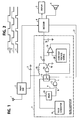
- radio-frequency paging signals detected by antenna 1 are fed into a receiver, or front end 2 in which the signals are converted into a form that can be digitally processed and applied to a decoder 4 of known circuitry.
- decoder 4 drives a display 5 for providing a display of received information and a loudspeaker 6 for alerting the user.
- Front end 2 is powered by a battery 3 and decoder 4, whose energy consumption varies significantly between active and inactive times, is powered by a DC-DC converter 7.
- DC-DC converter 7 is essentially a switching regulator and includes a pulse generator 10 that generates square-wave pulses "a” as shown in Fig. 2. This pulse signal is delayed by a predetermined amount by a delay circuit 11, producing a delayed pulse signal "b". These pulse signals are combined by an AND gate 12 to produce low duty-ratio pulses "c" in comparison with pulses "a".
- the high duty-ratio pulse signal from pulse generator 10 and the low duty-ratio pulse signal from AND gate 12 are supplied to the upper and lower positions of a switch 13, respectively, and one of the pulse signals is selectively applied to an AND gate 14 in accordance with the binary state of a load indicating signal which is supplied on lead 21 from decoder 4.
- the output of AND gate 14 is coupled to the base of a switching transistor 16 having an emitter-collector path connected between ground and one end of an inductor 15, the other end of which is coupled to battery 3.
- AND gate 14 is enabled, switching transistor 16 is gated on and off according to the duty cycle of the pulses from AND gate 14 to induce a damped oscillatory voltage across inductor 15 higher than the voltage from battery 3.
- This voltage is rectified by a diode 17 and a capacitor 18, coupled to the cathode of diode 17, is charged to store DC energy of a varying level according to the load.
- decoder 4 is sufficiently powered by this DC energy when processing the incoming signal and allows DC-DC converter 7 to decrease the amount of energy stored in capacitor 18 in the absence of incoming signals.
- comparator 19 To the cathode of diode 17 is coupled the negative input of a comparator 19, The positive input of comparator 19 is connected to a constant voltage source 20. By comparator 19 the voltage developed across capacitor 18 is compared with a prescribed reference voltage set by constant voltage source 20. A logic-0 output is produced by comparator 19 when the capacitor voltage is higher than the reference voltage, otherwise a logic-1 output is produced. The output of comparator 19 is applied to AND gate 14. Therefore, AND gate 14 is enabled when the voltage developed in capacitor 18 is lower than the reference voltage to supply DC energy thereto, and is advantageously disabled for power saving purposes when it is higher than the reference voltage.
- Decoder 4 generates a load indicating signal having a logic-1 state indicating that it is processing an incoming signal and a logic-0 state indicating that it is not processing signals.
- the load-indicating signal is at logic-1 state
- the contact of switch 13 is switched to the upper position for coupling the high duty-ratio pulse signal to AND gate 14. Otherwise, the switch is moved to the lower position for coupling the low duty-ratio pulse signal to AND gate 14.
- the amount of energy stored in capacitor 18 is proportional to the amount of current flowing through transistor 16, the DC energy stored in capacitor 18 increases when transistor 16 is gated with the high duty-ratio pulses and decreases when it is gated with the low duty-ratio pulses. Therefore, the stored energy increases in the presence of an incoming signal and decreases in the absence of an incoming signal.
Landscapes
- Engineering & Computer Science (AREA)
- Physics & Mathematics (AREA)
- Computer Networks & Wireless Communication (AREA)
- Electromagnetism (AREA)
- General Physics & Mathematics (AREA)
- Power Engineering (AREA)
- Dc-Dc Converters (AREA)
- Mobile Radio Communication Systems (AREA)
- Control Of Voltage And Current In General (AREA)
Claims (4)
- Gleichstromwandler für einen Funkrufempfänger mit einer von einer Batterie (3) versorgten Eingangsstufe (2), einem Decoder (4) zum Verarbeiten eines von der Eingangsstufe empfangenen hereinkommenden Signals, einem Oszillator (10 - 13) zum Erzeugen von Oszillatorimpulsen, einer mit der Batterie (3) verbundenen Induktivität (15), einem mit ihr verbundenen Schaltelement (16) zum Unterbrechen eines Stroms durch dieInduktivität als Antwort auf die Oszillatorimpulse, um eine Schwingspannung in der Induktivität zu erzeugen, einem Kondensator (18) und einer Diode (17) zum Gleichrichten der Schwingspannung und zum Laden des Kondensators (18) mit der gleichgerichteten Spannung, dadurch gekennzeichnet, daß der Decoder mit der Spannung versorgt wird, die durch den Kondensator (18) entwickelt wird, der mit der Induktivitätverbunden ist, um Gleichstromenergie zu speichern, die zur Dauer des Stroms proportional ist, und der ein erstes Signal, das einen aktiven Zustand des Decoders anzeigt, und ein zweites Signal, das einen inaktiven Zustand des Decoders anzeigt, erzeugt, wobei das Schaltelement auf jedes der ersten und zweiten Impulssignale anspricht, um zu ermöglichen, daß eine Spannung in der Induktivität entwickelt wird,daß der Oszillator (10 - 13) eine Erzeugungseinrichtung für variable Tastimpulse ist, die als Antwort auf das erste Signal ein erstes Impulssignal mit einem hohen Tastverhältnis und als Antwort auf das zweite Signal ein zweites Impulssignal mit einem niedrigen Tastverhältnis erzeugt, unddaß eine Energiespareinrichtung (14, 17, 19, 20) vorgesehen ist, um die durch den Kondensator (18) entwickelte Spannung mit einer Vergleichsspannung zu vergleichen und um zu verhindern, daß die Spannung in dem Kondensator über die Vergleichsspannung steigt.
- Gleichstromwandler nach Anspruch 1, dadurch gekennzeichnet, daß die Energiespareinrichtung aufweist:eine Gattereinrichtung (14), die zwischen die Erzeugungseinrichtung für variable Tastimpulse (10 - 13) und das Schaltelement (16) der spannungsinduzierenden Schaltung geschaltet ist, undeinen Komparator (19) zum Vergleichen der durch den Kondensator entwickelten Spannung mit der Vergleichsspannung und zum Veranlassen, daß die Gattereinrichtung (14) dem Schaltelement entweder das erste oder zweite Impulssignal zuführt, wenn die gespeicherte Spannung niedriger ist als die Vergleichsspannung, und zum Veranlassen, daß die Gattereinrichtung aufhört, dem Schaltelement das erste und das zweite Impulssignal zuzuführen, wenn die gespeicherte Spannung höher ist als die Vergleichsspannung.
- Gleichstromwandler nach Anspruch 1 oder 2, dadurch gekennzeichnet, daß das erste Impulssignal und das zweite Impulssignal die gleiche Impulsfolgefrequenz besitzen.
- Gleichstromwandler nach einem der Ansprüche 1, 2 oder 3, dadurch gekennzeichnet, daß die Erzeugungseinrichtung für variable Tastimpulse aufweist:einen Impulsgenerator zum Erzeugen des ersten Impulssignals;eine Verzögerungseinrichtung zum Verzögern des ersten Impulssignals; undeine Gattereinrichtung zum Kombinieren des ersten Impulssignals mit dem verzögerten Impulssignal, um das zweite Impulssignal zu erzeugen.
Applications Claiming Priority (2)
| Application Number | Priority Date | Filing Date | Title |
|---|---|---|---|
| JP201634/90 | 1990-07-30 | ||
| JP2201634A JPH0488870A (ja) | 1990-07-30 | 1990-07-30 | スイッチングレギュレータ回路 |
Publications (3)
| Publication Number | Publication Date |
|---|---|
| EP0469501A2 EP0469501A2 (de) | 1992-02-05 |
| EP0469501A3 EP0469501A3 (en) | 1992-04-15 |
| EP0469501B1 true EP0469501B1 (de) | 1996-11-20 |
Family
ID=16444330
Family Applications (1)
| Application Number | Title | Priority Date | Filing Date |
|---|---|---|---|
| EP91112688A Expired - Lifetime EP0469501B1 (de) | 1990-07-30 | 1991-07-29 | Energiesparende Gleichstromwandler für Funkrufempfänger |
Country Status (5)
| Country | Link |
|---|---|
| US (1) | US5193211A (de) |
| EP (1) | EP0469501B1 (de) |
| JP (1) | JPH0488870A (de) |
| AU (1) | AU648093B2 (de) |
| DE (1) | DE69123195T2 (de) |
Families Citing this family (26)
| Publication number | Priority date | Publication date | Assignee | Title |
|---|---|---|---|---|
| US5355518A (en) * | 1992-05-26 | 1994-10-11 | Kindinger Peter A | Receiver with constant battery saving duty cycle |
| US5448756A (en) * | 1992-07-02 | 1995-09-05 | Motorola, Inc. | High frequency battery saver for a radio receiver |
| JP2788827B2 (ja) * | 1992-07-29 | 1998-08-20 | 日本電気株式会社 | 無線選択呼出受信機 |
| DE4244352C2 (de) * | 1992-12-28 | 2003-04-17 | Heinz Lindenmeier | Schaltungsanordnung zur Gleichstromspeisung einer Antennenverstärkerschaltung |
| US5481178A (en) | 1993-03-23 | 1996-01-02 | Linear Technology Corporation | Control circuit and method for maintaining high efficiency over broad current ranges in a switching regulator circuit |
| FI94685C (fi) * | 1993-11-22 | 1995-10-10 | Nokia Mobile Phones Ltd | Avainnettu kytkintyyppinen virtalähde aikajakoisiin radiopuhelinjärjestelmiin |
| US5491445A (en) * | 1994-07-05 | 1996-02-13 | Delco Electronics Corporation | Booster power converter having accelerated transient boost response |
| US6775531B1 (en) * | 1994-07-21 | 2004-08-10 | Interdigital Technology Corporation | Subscriber terminal temperature regulation |
| KR100346503B1 (ko) * | 1994-07-21 | 2002-11-22 | 인터디지탈 테크날러지 코포레이션 | 통신시스템 가입자 유니트용 전력소비 제어방법 및 장치 |
| US6243399B1 (en) | 1994-07-21 | 2001-06-05 | Interdigital Technology Corporation | Ring signal generator |
| US5949226A (en) * | 1995-04-10 | 1999-09-07 | Kabushiki Kaisha Toyoda Jidoshokki Seisakush | DC/DC converter with reduced power consumpton and improved efficiency |
| JPH09215319A (ja) | 1996-02-01 | 1997-08-15 | Toyota Autom Loom Works Ltd | Dc/dcコンバータ |
| GB2314474B (en) * | 1996-06-21 | 2001-03-07 | Univ Bristol | Low power audio device |
| US5991635A (en) * | 1996-12-18 | 1999-11-23 | Ericsson, Inc. | Reduced power sleep modes for mobile telephones |
| US5912552A (en) | 1997-02-12 | 1999-06-15 | Kabushiki Kaisha Toyoda Jidoshokki Seisakusho | DC to DC converter with high efficiency for light loads |
| JPH10313572A (ja) | 1997-05-09 | 1998-11-24 | Toyota Autom Loom Works Ltd | スイッチングレギュレータ制御方式 |
| US6307356B1 (en) | 1998-06-18 | 2001-10-23 | Linear Technology Corporation | Voltage mode feedback burst mode circuit |
| US6127815A (en) | 1999-03-01 | 2000-10-03 | Linear Technology Corp. | Circuit and method for reducing quiescent current in a switching regulator |
| JP3425900B2 (ja) * | 1999-07-26 | 2003-07-14 | エヌイーシーマイクロシステム株式会社 | スイッチングレギュレータ |
| WO2002058217A2 (en) * | 2001-01-18 | 2002-07-25 | Koninklijke Philips Electronics N.V. | A single level time-shifted reference dc/dc converter |
| US6674274B2 (en) | 2001-02-08 | 2004-01-06 | Linear Technology Corporation | Multiple phase switching regulators with stage shedding |
| US6476589B2 (en) | 2001-04-06 | 2002-11-05 | Linear Technology Corporation | Circuits and methods for synchronizing non-constant frequency switching regulators with a phase locked loop |
| US7019507B1 (en) | 2003-11-26 | 2006-03-28 | Linear Technology Corporation | Methods and circuits for programmable current limit protection |
| US7030596B1 (en) | 2003-12-03 | 2006-04-18 | Linear Technology Corporation | Methods and circuits for programmable automatic burst mode control using average output current |
| CN101860180B (zh) * | 2009-04-08 | 2013-02-13 | 鸿富锦精密工业(深圳)有限公司 | Mos管驱动装置及电源模块 |
| CN103078498B (zh) * | 2012-12-27 | 2015-07-29 | 华为技术有限公司 | 一种电压转换电路及其使用方法 |
Family Cites Families (11)
| Publication number | Priority date | Publication date | Assignee | Title |
|---|---|---|---|---|
| US3953785A (en) * | 1974-11-29 | 1976-04-27 | Telxon Corporation | Power supply |
| JPS5652440U (de) * | 1979-09-29 | 1981-05-09 | ||
| DE3063190D1 (en) * | 1980-01-17 | 1983-06-16 | Autophon Ag | Portable paging receiver with a shift register and a direct current converter |
| GB8316352D0 (en) * | 1983-06-16 | 1983-07-20 | Motorola Inc | Dc-dc converter |
| US4536700A (en) * | 1984-03-28 | 1985-08-20 | United Technologies Corporation | Boost feedforward pulse width modulation regulator |
| US4634956A (en) * | 1985-01-10 | 1987-01-06 | Motorola, Inc. | DC to DC converter |
| US4755816A (en) * | 1986-10-29 | 1988-07-05 | Motorola Inc. | Battery saving method for a selective call radio paging receiver |
| US4814684A (en) * | 1987-09-30 | 1989-03-21 | Trw Inc. | Apparatus for extending the Vout/Vin ratio of a DC-to-DC converter |
| JPH0616601B2 (ja) * | 1988-09-07 | 1994-03-02 | 三洋電機株式会社 | 受信電波処理回路のパワーセイブ回路及びそのパワーセイブ方法 |
| US4955075A (en) * | 1988-10-17 | 1990-09-04 | Motorola, Inc. | Battery saver circuit for a frequency synthesizer |
| US5028861A (en) * | 1989-05-24 | 1991-07-02 | Motorola, Inc. | Strobed DC-DC converter with current regulation |
-
1990
- 1990-07-30 JP JP2201634A patent/JPH0488870A/ja active Pending
-
1991
- 1991-07-29 DE DE69123195T patent/DE69123195T2/de not_active Expired - Fee Related
- 1991-07-29 EP EP91112688A patent/EP0469501B1/de not_active Expired - Lifetime
- 1991-07-30 US US07/737,546 patent/US5193211A/en not_active Expired - Fee Related
- 1991-07-30 AU AU81496/91A patent/AU648093B2/en not_active Ceased
Non-Patent Citations (1)
| Title |
|---|
| "Transistor Technology" Journal, September 1989; page 520 * |
Also Published As
| Publication number | Publication date |
|---|---|
| EP0469501A3 (en) | 1992-04-15 |
| AU8149691A (en) | 1992-02-06 |
| DE69123195D1 (de) | 1997-01-02 |
| JPH0488870A (ja) | 1992-03-23 |
| EP0469501A2 (de) | 1992-02-05 |
| DE69123195T2 (de) | 1997-03-13 |
| US5193211A (en) | 1993-03-09 |
| AU648093B2 (en) | 1994-04-14 |
Similar Documents
| Publication | Publication Date | Title |
|---|---|---|
| EP0469501B1 (de) | Energiesparende Gleichstromwandler für Funkrufempfänger | |
| US5028861A (en) | Strobed DC-DC converter with current regulation | |
| US6580258B2 (en) | Control circuit and method for maintaining high efficiency over broad current ranges in a switching regulator circuit | |
| KR930005341B1 (ko) | Dc-dc 변환기 | |
| KR101254814B1 (ko) | 가변 피크 전류 및 가변 오프 시간 제어 기능을 구비한스위치드 변환기 | |
| US7880393B2 (en) | Power-saving circuit | |
| US4630186A (en) | Power source circuit | |
| EP0806078B1 (de) | Leistungsversorgungsschaltung | |
| US4573112A (en) | Switching regulator with a quiescent time period | |
| MXPA05004086A (es) | Suministro de energia acoplado capacitivamente. | |
| MY134537A (en) | Capacitively coupled power supply | |
| JPH11196540A (ja) | 電子機器 | |
| CA2038662C (en) | Apparatus for driving the armature of an electric stapler | |
| KR20010049751A (ko) | 버크 컨버터 | |
| US6016259A (en) | Power supply circuit | |
| JP2793806B2 (ja) | 電力変換制御装置 | |
| MXPA96004531A (en) | Power supply of tuned switch mode with control of corrie mode | |
| JP3525436B2 (ja) | スイッチング電源装置 | |
| US5650924A (en) | Electric power supply device for a monitor | |
| KR100355942B1 (ko) | 휴대용 단말기의 배터리에 전원을 공급하는 전원공급장치 | |
| JP3318773B2 (ja) | 電源装置 | |
| JP2000358368A (ja) | スイッチング電源装置 | |
| JP2814443B2 (ja) | スイッチング電源装置 | |
| JP2605317B2 (ja) | 高圧回路 | |
| JPH0442772A (ja) | スィツチング電源装置 |
Legal Events
| Date | Code | Title | Description |
|---|---|---|---|
| PUAI | Public reference made under article 153(3) epc to a published international application that has entered the european phase |
Free format text: ORIGINAL CODE: 0009012 |
|
| 17P | Request for examination filed |
Effective date: 19910828 |
|
| AK | Designated contracting states |
Kind code of ref document: A2 Designated state(s): DE GB NL |
|
| PUAL | Search report despatched |
Free format text: ORIGINAL CODE: 0009013 |
|
| AK | Designated contracting states |
Kind code of ref document: A3 Designated state(s): DE GB NL |
|
| 17Q | First examination report despatched |
Effective date: 19940811 |
|
| GRAH | Despatch of communication of intention to grant a patent |
Free format text: ORIGINAL CODE: EPIDOS IGRA |
|
| GRAH | Despatch of communication of intention to grant a patent |
Free format text: ORIGINAL CODE: EPIDOS IGRA |
|
| GRAA | (expected) grant |
Free format text: ORIGINAL CODE: 0009210 |
|
| AK | Designated contracting states |
Kind code of ref document: B1 Designated state(s): DE GB NL |
|
| REF | Corresponds to: |
Ref document number: 69123195 Country of ref document: DE Date of ref document: 19970102 |
|
| PGFP | Annual fee paid to national office [announced via postgrant information from national office to epo] |
Ref country code: GB Payment date: 19970723 Year of fee payment: 7 |
|
| PGFP | Annual fee paid to national office [announced via postgrant information from national office to epo] |
Ref country code: NL Payment date: 19970731 Year of fee payment: 7 |
|
| PLBE | No opposition filed within time limit |
Free format text: ORIGINAL CODE: 0009261 |
|
| STAA | Information on the status of an ep patent application or granted ep patent |
Free format text: STATUS: NO OPPOSITION FILED WITHIN TIME LIMIT |
|
| PGFP | Annual fee paid to national office [announced via postgrant information from national office to epo] |
Ref country code: DE Payment date: 19970930 Year of fee payment: 7 |
|
| 26N | No opposition filed | ||
| PG25 | Lapsed in a contracting state [announced via postgrant information from national office to epo] |
Ref country code: GB Free format text: LAPSE BECAUSE OF NON-PAYMENT OF DUE FEES Effective date: 19980729 |
|
| PG25 | Lapsed in a contracting state [announced via postgrant information from national office to epo] |
Ref country code: NL Free format text: LAPSE BECAUSE OF NON-PAYMENT OF DUE FEES Effective date: 19990201 |
|
| GBPC | Gb: european patent ceased through non-payment of renewal fee |
Effective date: 19980729 |
|
| NLV4 | Nl: lapsed or anulled due to non-payment of the annual fee |
Effective date: 19990201 |
|
| PG25 | Lapsed in a contracting state [announced via postgrant information from national office to epo] |
Ref country code: DE Free format text: LAPSE BECAUSE OF NON-PAYMENT OF DUE FEES Effective date: 19990501 |