EP0469401B1 - Verfahren zum Herstellen eines Halbleiterbauelementes durch Trockenätzung zweier aufgestapelten SiO2-Schichten - Google Patents
Verfahren zum Herstellen eines Halbleiterbauelementes durch Trockenätzung zweier aufgestapelten SiO2-Schichten Download PDFInfo
- Publication number
- EP0469401B1 EP0469401B1 EP91112056A EP91112056A EP0469401B1 EP 0469401 B1 EP0469401 B1 EP 0469401B1 EP 91112056 A EP91112056 A EP 91112056A EP 91112056 A EP91112056 A EP 91112056A EP 0469401 B1 EP0469401 B1 EP 0469401B1
- Authority
- EP
- European Patent Office
- Prior art keywords
- gas
- etching
- layer
- silicon oxide
- selection ratio
- Prior art date
- Legal status (The legal status is an assumption and is not a legal conclusion. Google has not performed a legal analysis and makes no representation as to the accuracy of the status listed.)
- Expired - Lifetime
Links
Images


Classifications
-
- H10P50/00—
-
- H10W20/092—
-
- H10P50/283—
-
- H10P95/064—
Definitions
- the present invention relates to a method of producing a semiconductor device, and more particularly to a reactive ion etching technique suitable for example for achieving a flat silicon oxide layer.
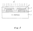
- Fig. 8 is a sectional view of a semiconductor device illustrating an example of a conventional method for flattening a silicon oxide layer in a semiconductor device.
- numeral 2 denotes an aluminum wiring formed by vapor deposition on an Si-substrate 1.
- An etchback method is employed for flattening a silicon oxide layer on this aluminum wiring. That is an SOG (spin-on-glass) layer 4 is applied on an SiO 2 layer 3 formed by a CVD method or thermal oxidation, and the SiO 2 layer 3 is subjected to dry etching together with the SOG layer 4 to achieve a flatness thereof by cutting off the surface to the broken line as shown in the figure.
- Such dry etching is rendered by sputter etching or ion milling using an inert Ar gas.
- the selection ratio of the SOG layer 4 (second silicon oxide layer) with respect to the foundation SiO 2 layer 3 (first silicon oxide layer) is about 1.18. The selection ratio is the ratio of the etching rate for different types of silicon oxide layers.
- EP-A-284124 A method for flattening superposed oxide layers is known from EP-A-284124, as well as from EP-A-249173.
- the present invention has been made to eliminate the above described problems, and its object is to provide a method of producing a semiconductor device in which a reduction in etching time and an improved yield with high reliability may be achieved by employing a dry etching method with a high etching rate while keeping the selection ratio low in the process for simultaneously etching a first silicon oxide layer and a different second silicon oxide layer.
- an SiO 2 layer 3 serving as a first silicon oxide layer is formed by a CVD method or thermal oxidation on the aluminum wiring 2 which has been formed by vapor deposition on an Si-substrate 1, and an SOG (spin-on-glass) layer 4 is applied by a spinner as a second silicon oxide layer onto the SiO 2 layer 3 having a ruggedness reflecting the steps in the aluminum wiring 2.
- a reactive ion etching is employed as the dry etching in an etchback process, a mixed gas consisting of a carbon fluoride gas such as C 2 F 6 and an inert gas such as He, Ar, Xe is used.
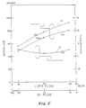
- Fig. 2 is a graph showing the relationship between the etching rate and selection ratio for various types of silicon oxide layers versus the mixing ratio of hexafluoroethane gas (C 2 F 6 ) and Ar gas. While in reality various types of silicon oxide layers are obtainable, a reactive ion etching in this example was effected by taking an SOG layer, a TEOS (tetra-ethoxy-ortho-silicate) layer, and an LTO (low temperature thermal oxidation SiO 2 ) layer as the representative examples.
- SOG SOG
- TEOS tetra-ethoxy-ortho-silicate
- LTO low temperature thermal oxidation SiO 2
- the etching rate was in general several hundreds nm/min (400 ⁇ 1000 nm/min). This is more than ten times greater than the etching rate in a conventional sputter etching or ion milling using AR gas.
- selection ratios on the basis of the SOG layer are also shown by solid lines 14, 15 (the right side vertical axis).
- the selection ratio for the TEOS layer and the selection ratio for the LTO layer were generally close to each other and they fell within the range of 1.12 ⁇ 1.17. When the mixing ratio was 50%, both of the selection ratios were about 1.12.
- Such selection ratio value is a value suitable for such in a flattening process and is by no means inferior to the selection ratio (1.18) according to a conventional sputtering or ion milling using Ar gas.
- the etching rate (left side vertical axis) and uniformity (right side vertical axis) for an SiO 2 layer formed by thermal oxidation were evaluated.
- the conditions were: 27 PA (200 mTorr) gas pressure, 17 seconds of etching time, 15 sccm of hexafluoroethane gas (C 2 F 6 ) and 135 sccm of Ar gas.
- a solid line 17 in Fig.3 the etching rate became higher with an increase in the RF power.
- the uniformity on the etched surface decreased gradually as shown by a solid line 16.
- an SiO 2 layer 3 of 600 nm thickness was formed by thermal oxidation on an aluminum wiring 2 formed by vapor deposition on the Si-substrate 1
- an SOG layer of 70 nm thickness was applied onto this SiO 2 layer 3 by a spinner, and thereafter an etchback was effected for about 18 seconds by reactive ion etching (RF power of 800W) using a mixed gas consisting of hexafluoroethane gas (C 2 F 6 : 15 sccm) and Ar gas (135 sccm).
- RF power of 800W reactive ion etching
- C 2 F 6 hexafluoroethane gas
- Ar gas (135 sccm
- argon gas was added in a reactive ion etching using a tetrafluoromethane gas (CF 4 ) and an octafluoropropane gas (C 3 F 8 ).
- Fig. 4 is a graph showing the relationship between the etching rate and selection ratio on the silicon oxide layer versus the mixing ratio between tetrafluoromethane gas (CF 4 ) and Ar gas
- Fig. 5 is a graph showing the relationship between the etching rate and selection ratio on the silicon oxide layer versus the mixing ratio between octafluoropropane gas (C 3 F 8 ) and Ar gas.
- the silicon oxide layers treated with reactive ion etching were an SOG layer and a TEOS layer.
- Example 2 the conditions were similar to Example 1, that is, the data on the etching rate (left side vertical axis) and the selection ratio on the basis of an SOG layer (right side vertical axis) were obtained by varying the mixing ratio (flow ratio) of tetrafluoromethane gas (CF 4 ), octafluoropropane gas (C 3 F 8 ) and Ar gas under the condition of a gas pressure of 27 Pa (200 mTorr), an RF power of 800 W, an etching time of 10 seconds and a total flow amount of 150 sccm per unit.
- CF 4 tetrafluoromethane gas
- C 3 F 8 octafluoropropane gas
- Ar gas Ar gas
- the etching rate on each layer was several hundreds nm/min (400 ⁇ 1000 nm/min) as shown in solid lines 18, 19, though it became lower with an increase in the proportion of Ar gas. Also, as shown by solid line 20, the selection ratio on the basis of an TEOS layer was within the range of 1.12 ⁇ 1.16 and the selection ratio with a 50% mixing ratio was about 1.12.
- the etching rate on each layer was also several hundreds nm/min (400 ⁇ 1000 nm/min as shown by solid lines 21, 22, though it became lower with an increase in the proportion of Ar gas. Further, as shown by solid line 23, the selection ratio on the basis of an TEOS layer was within the range of 1.12 ⁇ 1.16 and the selection ratio with a 50% mixing ratio was about 1.12.
- the etching rate was at the same level as in the case of using a mixed gas consisting of hexafluoroethane gas (C 2 F 6 ) and Ar gas, the etching rate being more than ten times greater than the etching rate of a conventional sputter etching or ion milling using Ar gas.
- the value of the selection ratio was at the same level as the selection ratio in the case of using a mixed gas consisting of hexafluoroethane gas (C 2 F 6 ) and Ar gas and was by no means inferior to the selection ratio (1.18) obtained by the conventional sputtering or ion milling using Ar gas.
- Example 2 investigations were conducted similar to Example 2 with respect to reactive ion etchings respectively using a mixed gas consisting of hexafluoroethane gas (C 2 F 6 ) and helium gas and a mixed gas consisting of hexafluoroethane gas (C 2 F 6 ) and xenon gas.
- a mixed gas consisting of hexafluoroethane gas (C 2 F 6 ) and helium gas a mixed gas consisting of hexafluoroethane gas (C 2 F 6 ) and xenon gas.
- the types of silicon oxide layers to be treated by reactive ion etching and the conditions of the reactive ion etching were the same as in Example 2.
- Fig. 6 is a graph showing the relationship between the etching rate (left side vertical axis) and selection ratio (right side vertical axis) versus the mixing ratio of hexafluoroethane gas (C 2 F 6 ) and He gas
- Fig. 7 is a graph showing the relationship between the etching rate (left side vertical axis) and selection ratio (right side vertical axis) versus the mixing ratio of hexafluoroethane gas (C 2 F 6 ) and Xe gas.
- the etching rate was also several hundreds nm/min (400 ⁇ 1000 nm/min) as shown by solid lines 24, 25, though it became lower with an increase in the proportion of He gas. Further, as shown by solid line 26, the selection ratio on the basis of an TEOS layer was within the range of 1.12 ⁇ 1.16 and the selection ratio with a 50% mixing ratio was about 1.12.
- the above described reactive ion etching may be applied not only to the flattening process in a multilayer interconnection but also to a co-etching process such as the groove-filling process of a trench which will be effected on two or more types of silicon oxide layers with a low selection ratio.
Landscapes
- Drying Of Semiconductors (AREA)
- Internal Circuitry In Semiconductor Integrated Circuit Devices (AREA)
Claims (2)
- Verfahren zum Nivellieren eines Halbleitersubstrats mit einer darauf ausgebildeten unebenen ersten Siliciumoxidschicht aus entweder Tetra-Ethoxy-Orthosilikat oder durch thermische Oxidation bei niedriger Temperatur ausgebildetem SiO2, umfassend die Schrittea) Bilden einer SOG-Schicht auf der ersten Siliciumoxidschicht als zweite Siliciumoxidschicht,b) Liefern einer Ätzgasmischung mit einer Gesamtströmung pro Mengeneinheit von 150 sccm, wobei die Gasmischung lediglich aus einem Kohlenstofffluoridgas, CnF2n + 2, wobei n eine ganze Zahl ist, und einem inerten Gas in einem Strömungsverhältnis von 15:135 bis 135:15 besteht,c) Schaffen eines Plasmas bei einem Gasdruck von 27 Pa und einer Hochfrequenzleistung von 800 W, wobei Fluorradikale in dem Plasma freigesetzt werden, undd) Zuführen der Fluorradikale zu einer Ätzoberfläche des Substrats, das aus Schritt a) resultiert, um die erste und die zweite Schicht in einem einzigen Ätzschritt trockenzuätzen.
- Verfahren nach Anspruch 1, bei dem das inerte Gas ein Gas oder eine Mischung aus zwei oder mehr Gasen ausgewählt aus He, Ar, Xe umfaßt.
Applications Claiming Priority (6)
| Application Number | Priority Date | Filing Date | Title |
|---|---|---|---|
| JP201811/90 | 1990-07-30 | ||
| JP20181190 | 1990-07-30 | ||
| JP20181190 | 1990-07-30 | ||
| JP7281191 | 1991-04-05 | ||
| JP72811/91 | 1991-04-05 | ||
| JP03072811A JP3092185B2 (ja) | 1990-07-30 | 1991-04-05 | 半導体装置の製造方法 |
Publications (2)
| Publication Number | Publication Date |
|---|---|
| EP0469401A1 EP0469401A1 (de) | 1992-02-05 |
| EP0469401B1 true EP0469401B1 (de) | 2000-11-02 |
Family
ID=26413950
Family Applications (1)
| Application Number | Title | Priority Date | Filing Date |
|---|---|---|---|
| EP91112056A Expired - Lifetime EP0469401B1 (de) | 1990-07-30 | 1991-07-18 | Verfahren zum Herstellen eines Halbleiterbauelementes durch Trockenätzung zweier aufgestapelten SiO2-Schichten |
Country Status (4)
| Country | Link |
|---|---|
| US (2) | US5173151A (de) |
| EP (1) | EP0469401B1 (de) |
| JP (1) | JP3092185B2 (de) |
| KR (1) | KR940007063B1 (de) |
Families Citing this family (62)
| Publication number | Priority date | Publication date | Assignee | Title |
|---|---|---|---|---|
| JP3092185B2 (ja) * | 1990-07-30 | 2000-09-25 | セイコーエプソン株式会社 | 半導体装置の製造方法 |
| US6238588B1 (en) * | 1991-06-27 | 2001-05-29 | Applied Materials, Inc. | High pressure high non-reactive diluent gas content high plasma ion density plasma oxide etch process |
| JPH05243402A (ja) * | 1992-03-03 | 1993-09-21 | Nec Corp | 半導体装置の製造方法 |
| US5549784A (en) * | 1992-09-04 | 1996-08-27 | Intel Corporation | Method for etching silicon oxide films in a reactive ion etch system to prevent gate oxide damage |
| US5331117A (en) * | 1992-11-12 | 1994-07-19 | Sgs-Thomson Microelectronics, Inc. | Method to improve interlevel dielectric planarization |
| TW243544B (de) * | 1992-12-31 | 1995-03-21 | At & T Corp | |
| US5384009A (en) * | 1993-06-16 | 1995-01-24 | Applied Materials, Inc. | Plasma etching using xenon |
| US5505816A (en) * | 1993-12-16 | 1996-04-09 | International Business Machines Corporation | Etching of silicon dioxide selectively to silicon nitride and polysilicon |
| US5461010A (en) * | 1994-06-13 | 1995-10-24 | Industrial Technology Research Institute | Two step etch back spin-on-glass process for semiconductor planarization |
| US6039851A (en) * | 1995-03-22 | 2000-03-21 | Micron Technology, Inc. | Reactive sputter faceting of silicon dioxide to enhance gap fill of spaces between metal lines |
| US5527736A (en) * | 1995-04-03 | 1996-06-18 | Taiwan Semiconductor Manufacturing Co. | Dimple-free tungsten etching back process |
| JP2956524B2 (ja) * | 1995-04-24 | 1999-10-04 | 日本電気株式会社 | エッチング方法 |
| US5717631A (en) * | 1995-07-21 | 1998-02-10 | Carnegie Mellon University | Microelectromechanical structure and process of making same |
| US5631197A (en) * | 1995-08-30 | 1997-05-20 | Taiwan Semiconductor Manufacturing Company, Ltd | Sacrificial etchback layer for improved spin-on-glass planarization |
| US5702981A (en) * | 1995-09-29 | 1997-12-30 | Maniar; Papu D. | Method for forming a via in a semiconductor device |
| US5650040A (en) * | 1995-11-30 | 1997-07-22 | Micron Technology, Inc. | Interfacial etch of silica to improve adherence of noble metals |
| US5780343A (en) * | 1995-12-20 | 1998-07-14 | National Semiconductor Corporation | Method of producing high quality silicon surface for selective epitaxial growth of silicon |
| US5821163A (en) * | 1996-02-13 | 1998-10-13 | Vlsi Technology, Inc. | Method for achieving accurate SOG etchback selectivity |
| US5930639A (en) * | 1996-04-08 | 1999-07-27 | Micron Technology, Inc. | Method for precision etching of platinum electrodes |
| KR100244793B1 (ko) * | 1996-05-01 | 2000-03-02 | 김영환 | 반도체 소자의 콘택홀 형성방법 |
| US5928967A (en) * | 1996-06-10 | 1999-07-27 | International Business Machines Corporation | Selective oxide-to-nitride etch process using C4 F8 /CO/Ar |
| US5945350A (en) * | 1996-09-13 | 1999-08-31 | Micron Technology, Inc. | Methods for use in formation of titanium nitride interconnects and interconnects formed using same |
| JP3808902B2 (ja) * | 1996-10-11 | 2006-08-16 | 東京エレクトロン株式会社 | プラズマエッチング方法 |
| US6362527B1 (en) * | 1996-11-21 | 2002-03-26 | Advanced Micro Devices, Inc. | Borderless vias on bottom metal |
| JPH10223608A (ja) * | 1997-02-04 | 1998-08-21 | Sony Corp | 半導体装置の製造方法 |
| US5856239A (en) * | 1997-05-02 | 1999-01-05 | National Semiconductor Corporaton | Tungsten silicide/ tungsten polycide anisotropic dry etch process |
| EP0893825A1 (de) * | 1997-07-23 | 1999-01-27 | STMicroelectronics S.r.l. | Planarisierungsmethode für integrierte Halbleiterschaltungen unter Verwendung von Mehrschichten |
| US6183655B1 (en) | 1997-09-19 | 2001-02-06 | Applied Materials, Inc. | Tunable process for selectively etching oxide using fluoropropylene and a hydrofluorocarbon |
| KR100528569B1 (ko) * | 1997-09-24 | 2005-11-15 | 인피니언 테크놀로지스 아게 | 실리콘 기판에 트렌치 구조물을 형성하는 방법 |
| US5920791A (en) * | 1997-11-06 | 1999-07-06 | Vanguard International Semiconductor Corporation | Method of manufacturing intermetal dielectrics for sub-half-micron semiconductor devices |
| KR100311487B1 (ko) * | 1997-12-16 | 2001-11-15 | 김영환 | 산화막식각방법 |
| TW388955B (en) * | 1998-08-19 | 2000-05-01 | United Microelectronics Corp | Recipe and method for removing silicon nitride |
| US6394104B1 (en) * | 1998-08-28 | 2002-05-28 | Taiwan Semiconductor Manufacturing Company | Method of controlling and improving SOG etchback etcher |
| JP3877109B2 (ja) | 1998-12-02 | 2007-02-07 | 富士通株式会社 | 半導体装置およびその製造方法 |
| US6797189B2 (en) | 1999-03-25 | 2004-09-28 | Hoiman (Raymond) Hung | Enhancement of silicon oxide etch rate and nitride selectivity using hexafluorobutadiene or other heavy perfluorocarbon |
| US6544429B1 (en) | 1999-03-25 | 2003-04-08 | Applied Materials Inc. | Enhancement of silicon oxide etch rate and substrate selectivity with xenon addition |
| US6461955B1 (en) * | 1999-04-29 | 2002-10-08 | Texas Instruments Incorporated | Yield improvement of dual damascene fabrication through oxide filling |
| JP4381526B2 (ja) * | 1999-10-26 | 2009-12-09 | 東京エレクトロン株式会社 | プラズマエッチング方法 |
| JP2003530184A (ja) | 2000-04-17 | 2003-10-14 | ビボメトリックス,インコーポレイテッド | 生理学的徴候を着装携行式にモニタするモニタ装置、システムおよび記録媒体 |
| US6511923B1 (en) * | 2000-05-19 | 2003-01-28 | Applied Materials, Inc. | Deposition of stable dielectric films |
| KR100366624B1 (ko) * | 2000-07-19 | 2003-01-09 | 삼성전자 주식회사 | 반사 방지막을 이용하는 반도체 소자 제조방법 |
| KR100379976B1 (ko) * | 2000-11-27 | 2003-04-16 | 삼성전자주식회사 | 실리콘 산화물 식각용 가스 조성물 및 이를 사용한 실리콘산화물의 식각 방법 |
| US20030168430A1 (en) * | 2002-03-11 | 2003-09-11 | Macronix International Co., Ltd. | Etching method with less waste gases |
| TWI278532B (en) * | 2002-06-23 | 2007-04-11 | Asml Us Inc | Method for energy-assisted atomic layer deposition and removal |
| AU2003245677A1 (en) * | 2002-06-23 | 2004-01-06 | Aviza Technology, Inc. | Method and system for atomic layer removal and atomic layer exchange |
| US7230292B2 (en) * | 2003-08-05 | 2007-06-12 | Micron Technology, Inc. | Stud electrode and process for making same |
| KR100536604B1 (ko) * | 2003-08-14 | 2005-12-14 | 삼성전자주식회사 | 고밀도 플라즈마 증착법을 이용한 갭필 방법 |
| US7457783B2 (en) | 2004-01-14 | 2008-11-25 | Panasonic Corporation | Import and export expense calculation apparatus |
| FR2866643B1 (fr) * | 2004-02-24 | 2006-05-26 | Saint Gobain | Substrat, notamment verrier, a surface hydrophobe, avec une durabilite amelioree des proprietes hydrophobes |
| US9492084B2 (en) | 2004-06-18 | 2016-11-15 | Adidas Ag | Systems and methods for monitoring subjects in potential physiological distress |
| US7307013B2 (en) * | 2004-06-30 | 2007-12-11 | Sandisk 3D Llc | Nonselective unpatterned etchback to expose buried patterned features |
| US9504410B2 (en) | 2005-09-21 | 2016-11-29 | Adidas Ag | Band-like garment for physiological monitoring |
| US7878979B2 (en) | 2005-05-20 | 2011-02-01 | Adidas Ag | Methods and systems for determining dynamic hyperinflation |
| US8033996B2 (en) | 2005-07-26 | 2011-10-11 | Adidas Ag | Computer interfaces including physiologically guided avatars |
| US8762733B2 (en) | 2006-01-30 | 2014-06-24 | Adidas Ag | System and method for identity confirmation using physiologic biometrics to determine a physiologic fingerprint |
| US8475387B2 (en) | 2006-06-20 | 2013-07-02 | Adidas Ag | Automatic and ambulatory monitoring of congestive heart failure patients |
| US9833184B2 (en) | 2006-10-27 | 2017-12-05 | Adidas Ag | Identification of emotional states using physiological responses |
| US7776623B2 (en) | 2008-06-30 | 2010-08-17 | Qualcomm Incorporated | System and method to fabricate magnetic random access memory |
| KR101105508B1 (ko) * | 2009-12-30 | 2012-01-13 | 주식회사 하이닉스반도체 | 반도체 메모리 소자의 제조 방법 |
| US9093389B2 (en) * | 2013-01-16 | 2015-07-28 | Applied Materials, Inc. | Method of patterning a silicon nitride dielectric film |
| US10879108B2 (en) * | 2016-11-15 | 2020-12-29 | Taiwan Semiconductor Manufacturing Co., Ltd. | Topographic planarization method for lithography process |
| TWI756003B (zh) * | 2021-01-04 | 2022-02-21 | 力晶積成電子製造股份有限公司 | 平坦化方法 |
Family Cites Families (9)
| Publication number | Priority date | Publication date | Assignee | Title |
|---|---|---|---|---|
| US4226665A (en) * | 1978-07-31 | 1980-10-07 | Bell Telephone Laboratories, Incorporated | Device fabrication by plasma etching |
| JPS5648140A (en) * | 1979-09-27 | 1981-05-01 | Seiko Epson Corp | Manufacture of semiconductor device |
| JPS59189633A (ja) * | 1983-04-13 | 1984-10-27 | Fujitsu Ltd | 半導体装置の製造方法 |
| US4676868A (en) * | 1986-04-23 | 1987-06-30 | Fairchild Semiconductor Corporation | Method for planarizing semiconductor substrates |
| US4676867A (en) * | 1986-06-06 | 1987-06-30 | Rockwell International Corporation | Planarization process for double metal MOS using spin-on glass as a sacrificial layer |
| NL8700541A (nl) * | 1987-03-06 | 1988-10-03 | Philips Nv | Werkwijze voor het vervaardigen van een halfgeleiderinrichting waarbij een plak silicium plaatselijk wordt voorzien van veldoxidegebieden. |
| US4962063A (en) * | 1988-11-10 | 1990-10-09 | Applied Materials, Inc. | Multistep planarized chemical vapor deposition process with the use of low melting inorganic material for flowing while depositing |
| EP0368504A3 (de) * | 1988-11-10 | 1990-09-12 | Applied Materials, Inc. | Planarisationsmethode für eine IC-Struktur |
| JP3092185B2 (ja) * | 1990-07-30 | 2000-09-25 | セイコーエプソン株式会社 | 半導体装置の製造方法 |
-
1991
- 1991-04-05 JP JP03072811A patent/JP3092185B2/ja not_active Expired - Fee Related
- 1991-07-18 EP EP91112056A patent/EP0469401B1/de not_active Expired - Lifetime
- 1991-07-23 KR KR1019910012574A patent/KR940007063B1/ko not_active Expired - Fee Related
- 1991-07-29 US US07/736,855 patent/US5173151A/en not_active Expired - Lifetime
-
1992
- 1992-12-21 US US07/994,563 patent/US5294294A/en not_active Expired - Lifetime
Also Published As
| Publication number | Publication date |
|---|---|
| US5173151A (en) | 1992-12-22 |
| JPH04218915A (ja) | 1992-08-10 |
| KR940007063B1 (ko) | 1994-08-04 |
| JP3092185B2 (ja) | 2000-09-25 |
| US5294294A (en) | 1994-03-15 |
| EP0469401A1 (de) | 1992-02-05 |
| KR920003437A (ko) | 1992-02-29 |
| HK1014296A1 (en) | 1999-09-24 |
Similar Documents
| Publication | Publication Date | Title |
|---|---|---|
| EP0469401B1 (de) | Verfahren zum Herstellen eines Halbleiterbauelementes durch Trockenätzung zweier aufgestapelten SiO2-Schichten | |
| US5814564A (en) | Etch back method to planarize an interlayer having a critical HDP-CVD deposition process | |
| US5035768A (en) | Novel etch back process for tungsten contact/via filling | |
| US5841196A (en) | Fluted via formation for superior metal step coverage | |
| US6605863B2 (en) | Low k film application for interlevel dielectric and method of cleaning etched features | |
| US20020142598A1 (en) | Plasma dielectric etch process using a long fluorocarbon | |
| US20050106888A1 (en) | Method of in-situ damage removal - post O2 dry process | |
| US6207570B1 (en) | Method of manufacturing integrated circuit devices | |
| KR100432984B1 (ko) | 텅스텐에대하여높은식각선택비를가지는등방성실리콘식각방법 | |
| KR20000023003A (ko) | 반도체 기판의 표면 평탄화 처리 방법 및 절연층에서의 전도 플러그 생성 처리 방법 | |
| US5639345A (en) | Two step etch back process having a convex and concave etch profile for improved etch uniformity across a substrate | |
| US20080023144A1 (en) | Dielectric etch tool configured for high density and low bombardment energy plasma providing high etch rates | |
| US20050136686A1 (en) | Gap-fill method using high density plasma chemical vapor deposition process and method of manufacturing integrated circuit device | |
| US6607985B1 (en) | Gate stack and etch process | |
| US6037278A (en) | Method of manufacturing semiconductor devices having multi-level wiring structure | |
| US6593241B1 (en) | Method of planarizing a semiconductor device using a high density plasma system | |
| US6114253A (en) | Via patterning for poly(arylene ether) used as an inter-metal dielectric | |
| US5575886A (en) | Method for fabricating semiconductor device with chemical-mechanical polishing process for planarization of interlayer insulation films | |
| US5167760A (en) | Etchback process for tungsten contact/via filling | |
| KR100670706B1 (ko) | 반도체 소자의 콘택 플러그 형성 방법 | |
| US6806185B2 (en) | Method for forming low dielectric constant damascene structure while employing a carbon doped silicon oxide capping layer | |
| US6214735B1 (en) | Method for planarizing a semiconductor substrate | |
| HK1014296B (en) | Method of producing a semiconductor device by dry etching two superposed sio2 layers | |
| US10937659B2 (en) | Method of anisotropically etching adjacent lines with multi-color selectivity | |
| US5920791A (en) | Method of manufacturing intermetal dielectrics for sub-half-micron semiconductor devices |
Legal Events
| Date | Code | Title | Description |
|---|---|---|---|
| PUAI | Public reference made under article 153(3) epc to a published international application that has entered the european phase |
Free format text: ORIGINAL CODE: 0009012 |
|
| 17P | Request for examination filed |
Effective date: 19910718 |
|
| AK | Designated contracting states |
Kind code of ref document: A1 Designated state(s): DE FR GB NL |
|
| 17Q | First examination report despatched |
Effective date: 19940830 |
|
| GRAG | Despatch of communication of intention to grant |
Free format text: ORIGINAL CODE: EPIDOS AGRA |
|
| RTI1 | Title (correction) |
Free format text: METHOD OF PRODUCING A SEMICONDUCTOR DEVICE BY DRY ETCHING TWO SUPERPOSED SIO2 LAYERS |
|
| RTI1 | Title (correction) |
Free format text: METHOD OF PRODUCING A SEMICONDUCTOR DEVICE BY DRY ETCHING TWO SUPERPOSED SIO2 LAYERS |
|
| GRAG | Despatch of communication of intention to grant |
Free format text: ORIGINAL CODE: EPIDOS AGRA |
|
| GRAH | Despatch of communication of intention to grant a patent |
Free format text: ORIGINAL CODE: EPIDOS IGRA |
|
| GRAH | Despatch of communication of intention to grant a patent |
Free format text: ORIGINAL CODE: EPIDOS IGRA |
|
| RBV | Designated contracting states (corrected) |
Designated state(s): GB |
|
| GRAA | (expected) grant |
Free format text: ORIGINAL CODE: 0009210 |
|
| AK | Designated contracting states |
Kind code of ref document: B1 Designated state(s): GB |
|
| EN | Fr: translation not filed | ||
| PLBE | No opposition filed within time limit |
Free format text: ORIGINAL CODE: 0009261 |
|
| STAA | Information on the status of an ep patent application or granted ep patent |
Free format text: STATUS: NO OPPOSITION FILED WITHIN TIME LIMIT |
|
| 26N | No opposition filed | ||
| REG | Reference to a national code |
Ref country code: GB Ref legal event code: IF02 |
|
| PGFP | Annual fee paid to national office [announced via postgrant information from national office to epo] |
Ref country code: GB Payment date: 20060712 Year of fee payment: 16 |
|
| GBPC | Gb: european patent ceased through non-payment of renewal fee |
Effective date: 20070718 |
|
| PG25 | Lapsed in a contracting state [announced via postgrant information from national office to epo] |
Ref country code: GB Free format text: LAPSE BECAUSE OF NON-PAYMENT OF DUE FEES Effective date: 20070718 |