EP0467682A2 - Treiberschaltung für eine Halbleitervorrichtung der spannungsgesteuerten Art - Google Patents
Treiberschaltung für eine Halbleitervorrichtung der spannungsgesteuerten Art Download PDFInfo
- Publication number
- EP0467682A2 EP0467682A2 EP91306553A EP91306553A EP0467682A2 EP 0467682 A2 EP0467682 A2 EP 0467682A2 EP 91306553 A EP91306553 A EP 91306553A EP 91306553 A EP91306553 A EP 91306553A EP 0467682 A2 EP0467682 A2 EP 0467682A2
- Authority
- EP
- European Patent Office
- Prior art keywords
- semiconductor device
- voltage
- circuit
- drive circuit
- overcurrent
- Prior art date
- Legal status (The legal status is an assumption and is not a legal conclusion. Google has not performed a legal analysis and makes no representation as to the accuracy of the status listed.)
- Withdrawn
Links
Images


Classifications
-
- H—ELECTRICITY
- H03—ELECTRONIC CIRCUITRY
- H03K—PULSE TECHNIQUE
- H03K17/00—Electronic switching or gating, i.e. not by contact-making and –breaking
- H03K17/51—Electronic switching or gating, i.e. not by contact-making and –breaking characterised by the components used
- H03K17/78—Electronic switching or gating, i.e. not by contact-making and –breaking characterised by the components used using opto-electronic devices, i.e. light-emitting and photoelectric devices electrically- or optically-coupled
- H03K17/785—Electronic switching or gating, i.e. not by contact-making and –breaking characterised by the components used using opto-electronic devices, i.e. light-emitting and photoelectric devices electrically- or optically-coupled controlling field-effect transistor switches
-
- H—ELECTRICITY
- H03—ELECTRONIC CIRCUITRY
- H03K—PULSE TECHNIQUE
- H03K17/00—Electronic switching or gating, i.e. not by contact-making and –breaking
- H03K17/08—Modifications for protecting switching circuit against overcurrent or overvoltage
- H03K17/082—Modifications for protecting switching circuit against overcurrent or overvoltage by feedback from the output to the control circuit
- H03K17/0822—Modifications for protecting switching circuit against overcurrent or overvoltage by feedback from the output to the control circuit in field-effect transistor switches
-
- H—ELECTRICITY
- H03—ELECTRONIC CIRCUITRY
- H03K—PULSE TECHNIQUE
- H03K17/00—Electronic switching or gating, i.e. not by contact-making and –breaking
- H03K17/08—Modifications for protecting switching circuit against overcurrent or overvoltage
- H03K17/082—Modifications for protecting switching circuit against overcurrent or overvoltage by feedback from the output to the control circuit
- H03K17/0828—Modifications for protecting switching circuit against overcurrent or overvoltage by feedback from the output to the control circuit in composite switches
-
- H—ELECTRICITY
- H03—ELECTRONIC CIRCUITRY
- H03K—PULSE TECHNIQUE
- H03K2217/00—Indexing scheme related to electronic switching or gating, i.e. not by contact-making or -breaking covered by H03K17/00
- H03K2217/0036—Means reducing energy consumption
Definitions
- the present invention relates to a drive circuit for a voltage driven type semiconductor device such as an IGBT (Insulated Gate Bipolar Transistors) or MOSFET, and in particular to a drive circuit having an overcurrent protection function that can protect the semiconductor device from an overcurrent fault caused by a short circuit or the like in a power conversion apparatus such as an inverter.
- a voltage driven type semiconductor device such as an IGBT (Insulated Gate Bipolar Transistors) or MOSFET
- Figs. 1A and 1B are views illustrating the basic operation of a conventional overcurrent protection circuit of this type:
- Fig. 1A is a block diagram showing a gate drive system of a power conversion apparatus;
- Fig. 1B is a diagram showing an equivalent circuit illustrating a voltage and current applied to a semiconductor device during a short circuit fault.
- IGBT an example of a voltage driven type semiconductor device, and the same reference characters designate the same or corresponding parts throughout the drawings.
- a gate voltage V GE from a gate drive circuit 1 which turns on and off the IGBT Q1 in response to a drive signal V DR fed from a PWM control circuit 2.
- the IGBT Q1 is a member constituting a three-phase bridge as shown in Fig. 4A.
- a voltage and current will be applied to the IGBT Q1 as shown in Fig. 1B: a short circuit current Ic flows from collector to emitter in the IGBT Q1 with a direct voltage Ed being applied thereto via a wire inductance L.
- the short circuit current Ic reaches four to five times the rated DC current of the IGBT Q1, or even about ten times the rated current in a high withstanding voltage device.
- the instantaneous power applied to the IGBT Q1 during the short circuit period is extremely large, and hence, the IGBT must be turned off through the gate in a short time (less than about 10 ⁇ sec) to cut off the overcurrent after the short circuit takes place. For this reason, an overcurrent protective function is incorporated in the gate drive circuit.
- Fig. 2 is a circuit diagram showing an example of a conventional gate drive circuit with an overcurrent protection function.
- reference character Q1 designates an IGBT as a main switching device
- PH1 denotes a photocoupler for isolating a drive signal V DR applied from a control circuit not shown in this figure
- V1 denotes a voltage source for supplying an on-gate voltage
- V2 designates a voltage source for supplying an off-gate voltage.
- a transistor T1 turns off, thereby turning a transistor T2 on and a transistor T3 off.
- the on-gate voltage V1 is applied across the gate and emitter of the IGBT Q1 through a gate resistor R G .
- a transistor T11 turns off, by which a base current tries to flow in the transistor T4 through a resistor R11 and a Zener diode ZD1.
- the on-timing of the transistor T4, however, is delayed by a capacitor C1 connected to the collector of the transistor T11.
- the on-voltage applied across the gate-emitter of the IGBT Q1 turns on the IGBT Q1, and so the collector-to-emitter voltage V CE of the IGBT Q1 drops to the on-voltage V CE (on).
- the voltage of the positive terminal of the capacitor C1 i.e., the voltage of the cathode of the Zener diode ZD1 is dropped to the on state voltage of the IGBT Q1 via a diode D1.
- the transistor T4 is maintained at the OFF state by selecting components to satisfy the following inequality.
- V ZD1 is the Zener voltage of the Zener diode ZD1
- V BE (T4) is the V BE of the transistor T4
- V F (D1) is the forward voltage of the diode D1.
- the transistor T1 is made on, which turns the transistor T2 off and the transistor T3 off.
- the IGBT Q1 is turned off because of the off-gate voltage V2 applied across the gate and emitter of the IGBT Q1 through the gate resistor RG.
- the transistor T11 is made on, which discharges the capacitor C1 to prepare the next turn-on operation of the IGBT Q1.
- the delay time Td is provided to delay the on-timing of the transistor T4 until the IGBT Q1 has completes turning on, thereby to prevent an overcurrent protective transistor T4 from being turned on during the normal operation. Accordingly, the delay time Td is called "turn-on confirming time" hereinafter.
- the gate-to-emitter voltage V GE of the IGBT Q1 declines with elapsing of time in accordance with the voltage of the capacitor C2, which is different from the normal turn-off operation as indicated by the solid line after time t2 in Fig. 3C.
- the reduction rate of the collector current Ic becomes small, thereby preventing a spike voltage V CEP of the V CE during the current interruption.
- broken lines in Fig. 3C represent waveforms when an overcurrent is cut off by directly adding the off-gate voltage V2 to the gate of IGBT Q1.
- the capacitor C1 (as a turn-on confirming timer) provides the turn-on confirming time Td to delay the on-timing of the transistor T4.
- the gate voltage V GE of the IGBT Q1 does not begin to decline until time t2 at which the transistor T4 conducts even when an overcurrent begins to flow at preceding time t1 as shown in Figs. 3A.
- the gate voltage declines, and interrupts the IGBT Q1 when it reduces below the threshold voltage V GE (th) of the IGBT.
- the turn-on confirming time Td must be set relatively long in the conventional circuit. This will be described in more detail below.
- Figs. 4A and 4B are views illustrating the turnon operation of IGBTs in an inverter:
- Fig. 4A is a circuit diagram of a main circuit of the inverter; and
- Fig. 4B is a diagram illustrating waveforms of the turn-on operation of the IGBT.
- reference character C0 denotes a smoothing capacitor constituting the direct current voltage source Ed
- Q1 Q11-Q16
- D0 D01-D06
- Fig. 3A illustrates waveforms of the IGBT operation when the drive signal V DR fed from the PWM control circuit 2 to the gate drive circuit 1 has a broad pulsewidth
- Fig. 3B illustrates waveforms of the IGBT operation when the drive signal V DR has a narrow pulsewidth.
- the soft interruption means turning off the IGBT slowly so as to prevent a counterelectromotive force caused by the wire inductance L.
- the soft interruption is accomplished by slowly decreasing the gate voltage V GE .
- the soft interruption works normally when a pulsewidth of the drive signal V DR is broad enough to continue beyond a term T W that begins at time tl when a short circuit fault occurs and terminates at time t3 when an overcurrent is interrupted, thereby turning off the IGBT Q1 safely as shown in Fig. 3A.
- a drive circuit for a voltage driven type semiconductor device comprising: a photocoupler which is turned on and off by a drive signal fed from an external control circuit; a pair of output transistors whose bases are connected each other, and are operatively connected to an output of the photocoupler; a voltage driven type semiconductor device which has a control terminal, a first main terminal, and a second main terminal, the control terminal and the first main terminal being supplied with control signals from outputs of the output transistors, and the first main terminal and the second terminal being made conductive or nonconductive by the control signals; a serial circuit of a resistor and a Zener diode, a first terminal of the serial circuit being connected to the second main terminal of the semiconductor device so that the serial circuit conducts when a voltage across the first and second main terminals of the semiconductor device exceeds a predetermined voltage; means for detecting, after a predetermined time has elapsed since the output of the photocoupler is produced to turn on the semiconductor device, the presence of the
- the drive circuit for a voltage driven type semiconductor device may further comprise a diode connected between the control terminal of the semiconductor device and the variable voltage source so as to shunt a displacement current produced by an overcurrent applied to the semiconductor device.
- the drive circuit for a voltage driven type semiconductor device may further comprise a transistor which is induced to turn on by the voltage decline of the variable voltage source so as to shortcircuit between the control terminal and the first main terminal of the semiconductor device to shunt a displacement current produced by an overcurrent applied to the semiconductor device.
- the drive circuit for a voltage driven type semiconductor device may further comprise means for latching the output of the photocoupler so as to hold the semiconductor device in an on state after detection of the means for detecting.
- the drive circuit for a voltage driven type semiconductor device may further comprise means for latching the output of the photocoupler so as hold the semiconductor device in an on state based on detection of the means for detecting for a predetermined period after the drive signal changes.
- the present invention includes the serial circuit of the resistor and Zener diode whose terminal is connected to the output terminal of the voltage driven type semiconductor device (the collector in the case of the IGBT), and detects an overcurrent by determining whether an excessive forward voltage drop exists on the basis of the presence and absence of a current flowing in the serial circuit, and simultaneously by detecting the presence of the drive signal V DR after the turn-on confirming time. In addition, once the overcurrent is detected, the overcurrent protection operation ignores the elimination of the drive signal V DR .
- a voltage of the Zener diode can be selected independently of a voltage supplied to the gate drive circuit. This makes it possible to set a detection level of the overcurrent at a high level, which can shorten a time required to detect the overcurrent, and hence the turn-on confirming time, thereby reducing energy consumed by the semiconductor device during the short circuit fault.
- the overcurrent operation ignores the change in (elimination of) the drive signal V DR during the overcurrent
- the overcurrent flowing in the semiconductor device can be softly interrupted independently of the pulsewidth of the drive signal V DR and the timing of a short circuit fault. This makes it possible to positively protect the semiconductor device from the overcurrent.
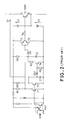
- Fig. 5 is a circuit diagram showing a drive circuit for a semiconductor device as a first embodiment of the present invention.
- the normal switching operation is similar to that of the conventional drive circuit of Fig. 2: the switching operation is carried out by a transistor T1 receiving the output signal of a photocoupler PH1, and a transistors T2 and T3 connected to the transistor T1.
- the drive circuit of this embodiment differs from that of Fig. 2 in that it has a variable voltage source 100 including serially connected transistors T4 and T5.
- the transistor T5 detects the presence and absence of the drive signal V DR fed from the control circuit 2 of Fig. 1A, and provides a turn-on confirming time Td determined by a capacitor C1 and a resistor R11 to ensure the turn-on of the IGBT Q1 when the drive signal V DR rises at time t30 in Fig.
- the transistor T4 detects the terminal voltage or the collector-to-emitter voltage V CE of the IGBT Q1 by using a serial circuit of resistors R5 and R6, and a Zener diode ZD1, which is connected to the output (collector) terminal of the IGBT Q1.
- the transistor T4 turns on when it detects a current flowing in the resistor R5. Accordingly, when the voltage V CE increases owing to an short circuit fault, the transistor T4 detects it and turns on.
- the serial circuit of the transistors T4 and T5 discharges the capacitor C2 only when the terminal voltage V CE increases by a short circuit fault or the like during the IGBT Q1 is in the ON state.
- the conventional turn-on confirming time Td must be greater than time t12 because the terminal voltage V CE becomes less than the conventional detection level Vth only after the time t12.
- the detection level of the present embodiment can be arbitrarily selected independent of the supply voltage to the gate drive circuit.
- the turn-on confirming time Td slightly larger than time t11 can be set.
- the freewheeling diode serially connected with the IGBT Q1 in a serial arm of the three-phase inverter bridge is maintained in a short circuit state until time t11 or t31 in Fig. 6 when the reverse recovery of the freewheeling diode has been completed. Even if a short circuit fault takes place, the behavior of the collector current Ic is the same as that of this normal turn-on state until the time t11 or t31. Accordingly, an overcurrent during a short circuit fault can be detected slightly after the time t11, and the overcurrent protection operation is started by this detection. Thus, the overcurrent of the IGBT Q1 can be interrupted even during the turn-on time from t11 to t12, and hence the IGBT Q1 is positively protected.
- the overcurrent protection operation of the drive circuit of Fig. 5 is as follows:
- the photocoupler PH1 is in the ON state, transistors T1 and T11 are in the OFF state, the transistor T2 is in the ON state and the transistor T3 is in the OFF state.
- an on-gate voltage V1 is applied across the gate and emitter of the IGBT Q1 through a gate resistor R G .
- the transistor T11 since the transistor T11 is in the OFF state, a base current of the transistor T5 that detects the presence of the drive signal V DR and provides the turn-on confirming time Td tries to flow from the resistor R11.
- the base current cannot flow in the transistor T5 because the transistor T4 which detects the collector-to-emitter voltage V CE and is serially connected to the transistor T5 is maintained in the OFF state because the voltage V CE of the IGBT Q1 is low, and hence no current flows through the resistor R5.
- the capacitor C2 serving as a variable voltage source 100 is not discharged (time t31-t32 in Fig. 6).
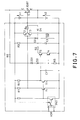
- Fig. 7 is a circuit diagram showing an arrangement of a gate drive circuit as a second embodiment of the present invention.
- a capacitor C2 constituting a variable voltage source 100 is connected to the gate G of an IGBT Q1 via a diode D4 for shunting a displacement current that pours into a IGBT Q1 via a junction capacity (not shown in Fig. 7) of the IGBT Q1 when an increasing collector-to-emitter voltage V CE is applied to the IGBT Q1.
- the diode D4 shunts the displacement current so as to prevent rising of the gate voltage V GE of the Q1, which serves to shorten the turn-off time of the IGBT Q1.
- Fig. 8 is a circuit diagram showing an arrangement of a gate drive circuit as a third embodiment of the present invention. This embodiment is provided, in addition to the circuit of Fig. 5, with a PNP transistor T6.
- the transistor T6 turns on as the voltage of a capacitor C2 making up a variable voltage source 100 declines, thereby shunting a displacement current.
- the transistor T6 shortcircuits the gate and emitter of the IGBT Q1 so as to prevent increase of the gate voltage V GE of IGBT Q1 due to the displacement current.
- Fig. 9 is a circuit diagram showing an arrangement of a gate drive circuit as a fourth embodiment of the present invention.
- This embodiment is provided, in addition to the circuit of Fig. 5, with a resistor R7 inserted in the discharge path of the capacitor C2, and a transistor T7 whose base is connected to the resistor R7.
- the transistor T7 turns on during the overcurrent protection operation because of the discharge current of a capacitor C2 flowing through the resistor R7.
- the output of a photocoupler PH1 is shortcircuited so that the protection operation is maintained even when the drive signal V DR is eliminated.
- Fig. 10 is a circuit diagram showing an arrangement of a gate drive circuit as a fifth embodiment of the present invention.
- This embodiment is provided, in addition to the circuit of Fig. 9, with a capacitor C3 inserted in the collector circuit of a transistor T7.
- the capacitor C3 is discharged through a discharge circuit composed of a photocoupler PH1, a resistor R8 and a diode D5.
- the capacitor C3 is charged by a current flowing through a resistor connected to the collector of a photodetector PH1 and the transistor T7.
- the capacitor C3 is gradually charged so that transistors T1 and T11 are turned on, resulting in making an IGBT Q1 off at a predetermined time after the change of the drive signal.
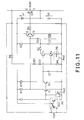
- Fig. 11 is a circuit diagram showing an arrangement of a gate drive circuit as a sixth embodiment of the present invention.
- This embodiment is provided, instead of the resistor R7 and the transistor T7 of Fig. 9, with a photocoupler PH2.
- a light emitting diode PD of the photocoupler PH2 is inserted in the discharging circuit of a capacitor C2, and an output transistor PT of the photocoupler PH2 shortcircuits the output of the photocoupler PH1.
- the operation of the embodiment is similar to that of the embodiment 4, and the protection operation functions independently of the change of the drive signal V DR .
Landscapes
- Power Conversion In General (AREA)
- Electronic Switches (AREA)
- Inverter Devices (AREA)
- Dc-Dc Converters (AREA)
Applications Claiming Priority (2)
| Application Number | Priority Date | Filing Date | Title |
|---|---|---|---|
| JP2191058A JP2669117B2 (ja) | 1990-07-19 | 1990-07-19 | 電圧駆動形半導体素子の駆動回路 |
| JP191058/90 | 1990-07-19 |
Publications (2)
| Publication Number | Publication Date |
|---|---|
| EP0467682A2 true EP0467682A2 (de) | 1992-01-22 |
| EP0467682A3 EP0467682A3 (en) | 1992-05-06 |
Family
ID=16268190
Family Applications (1)
| Application Number | Title | Priority Date | Filing Date |
|---|---|---|---|
| EP19910306553 Withdrawn EP0467682A3 (en) | 1990-07-19 | 1991-07-18 | Drive circuit for voltage driven type semiconductor device |
Country Status (3)
| Country | Link |
|---|---|
| US (1) | US5200879A (de) |
| EP (1) | EP0467682A3 (de) |
| JP (1) | JP2669117B2 (de) |
Cited By (11)
| Publication number | Priority date | Publication date | Assignee | Title |
|---|---|---|---|---|
| FR2705508A1 (fr) * | 1993-05-14 | 1994-11-25 | Fahrzeugklimaregelung Gmbh | Montage pour la mise en circuit et hors circuit d'un consommateur d'énergie électrique. |
| EP0643485A1 (de) * | 1993-09-09 | 1995-03-15 | Siemens Aktiengesellschaft | Schaltungsanordnung zum sanften Abschalten eines MOS-Halbleiterbauelementes bei Überstrom |
| EP0680146A3 (de) * | 1994-04-27 | 1996-07-17 | Sharp Kk | Treiberschaltung für ein Leistungsbauelement. |
| GB2268012B (en) * | 1992-06-18 | 1996-08-07 | Int Rectifier Corp | Method and apparatus for short circuit protection of power transistor device |
| DE19638619A1 (de) * | 1996-09-20 | 1998-04-02 | Siemens Ag | Vorrichtung zur Verminderung der Kurzschlußamplitude eines abschaltbaren, nichteinrastenden, MOS-gesteuerten Leistungshalbleiters |
| WO2000016481A3 (de) * | 1998-09-14 | 2000-07-13 | Siemens Ag | Schutzverfahren für ein steuerbares nicht einrastendes halbleiter-schaltelement und hierzu korrespondierende schutzschaltung |
| EP1054511A3 (de) * | 1999-04-27 | 2002-02-06 | DaimlerChrysler Rail Systems GmbH | Verfahren zur Überstromabschaltung eines Bipolartransistors mit isoliert angeordneter Gateelektrode (IGBT) und Vorrichtung zur Durchführung des Verfahrens |
| EP1635463A3 (de) * | 2004-09-14 | 2007-04-25 | Delphi Technologies, Inc. | Diskrete Schaltung zur Ansteuerung von Feldeffekttransistoren |
| CN103907275A (zh) * | 2011-11-15 | 2014-07-02 | 住友电气工业株式会社 | 晶体管保护电路 |
| WO2017003682A3 (en) * | 2015-06-30 | 2017-03-09 | Microsoft Technology Licensing, Llc | Analog limit on digitally set pulse widths |
| KR20210022572A (ko) * | 2018-06-21 | 2021-03-03 | 텍사스 인스트루먼츠 인코포레이티드 | 드라이버 및 슬루율-제어 회로 |
Families Citing this family (21)
| Publication number | Priority date | Publication date | Assignee | Title |
|---|---|---|---|---|
| JP2777307B2 (ja) * | 1992-04-28 | 1998-07-16 | 株式会社東芝 | 短絡保護回路 |
| US5418673A (en) * | 1992-12-14 | 1995-05-23 | North American Philips Corporation | Control electrode disable circuit for power transistor |
| US5424897A (en) * | 1993-04-05 | 1995-06-13 | Motorola, Inc. | Three leaded protected power device having voltage input |
| US5444595A (en) * | 1993-09-27 | 1995-08-22 | Nippondenso Co., Ltd. | Load drive apparatus including power transistor protection circuit from overcurrent |
| JPH07121252A (ja) * | 1993-10-26 | 1995-05-12 | Rohm Co Ltd | 安定化電源回路内蔵ic |
| DE4337504B4 (de) * | 1993-11-03 | 2005-04-28 | Sms Elotherm Gmbh | Verfahren und Vorrichtung zur Ansteuerung von abschaltbaren Leistungshalbleitern eines Resonanz-Umrichters mit angepaßter Schaltgeschwindigkeit |
| CA2172890C (en) * | 1995-06-06 | 2005-02-22 | Harold R. Schnetzka | Switch driver circuit |
| US6057998A (en) | 1996-12-25 | 2000-05-02 | Hitachi, Ltd. | Insulated gate type semiconductor apparatus with a control circuit |
| US6717785B2 (en) * | 2000-03-31 | 2004-04-06 | Denso Corporation | Semiconductor switching element driving circuit |
| US7236340B2 (en) * | 2002-02-11 | 2007-06-26 | International Rectifier Corporation | Gate control circuit for prevention of turn-off avalanche of power MOSFETs |
| JP4742313B2 (ja) * | 2006-03-22 | 2011-08-10 | 富士電機株式会社 | 電力変換装置の保護方式 |
| FI120812B (fi) * | 2007-04-30 | 2010-03-15 | Vacon Oyj | Tehopuolijohdekytkimen ohjaus |
| US7570101B1 (en) * | 2008-02-27 | 2009-08-04 | The United States Of America As Represented By The United States Department Of Energy | Advanced insulated gate bipolar transistor gate drive |
| US8884682B2 (en) * | 2011-04-04 | 2014-11-11 | Renesas Electronics Corporation | Power semiconductor device |
| CN108934095B (zh) * | 2017-05-22 | 2021-07-13 | 佛山市顺德区美的电热电器制造有限公司 | 电磁加热系统、igbt的驱动控制电路及其的故障检测方法 |
| CN108966394B (zh) * | 2017-05-22 | 2021-03-19 | 佛山市顺德区美的电热电器制造有限公司 | 电磁加热系统、igbt的驱动控制电路及其的故障检测方法 |
| CN108966395B (zh) * | 2017-05-22 | 2021-03-19 | 佛山市顺德区美的电热电器制造有限公司 | 电磁加热系统、igbt的驱动控制电路及其的故障检测方法 |
| CN108966396B (zh) * | 2017-05-22 | 2021-03-19 | 佛山市顺德区美的电热电器制造有限公司 | 电磁加热系统、igbt的驱动控制电路及其的故障检测方法 |
| EP4191856A4 (de) * | 2020-09-04 | 2024-01-24 | Sunwoda Mobility Energy Technology Co., Ltd. | Aktive klemmenschutzschaltung mit sanftem abschalten und stromversorgungssystem |
| GB2602132B (en) | 2020-12-18 | 2024-10-09 | Murata Manufacturing Co | Three output DC voltage supply with short circuit protection |
| US12184270B2 (en) * | 2023-01-17 | 2024-12-31 | Rosemount Aerospace Inc. | IGBT/MOSFET desaturation circuity w/ reverse polarity protection |
Family Cites Families (3)
| Publication number | Priority date | Publication date | Assignee | Title |
|---|---|---|---|---|
| EP0190925B1 (de) * | 1985-02-08 | 1993-12-29 | Kabushiki Kaisha Toshiba | Schutzschaltung für einen Bipolartransistor mit isoliertem Gate |
| DE68925163T2 (de) * | 1988-08-12 | 1996-08-08 | Hitachi Ltd | Treiberschaltung für Transistor mit isoliertem Gate; und deren Verwendung in einem Schalterkreis, einer Stromschalteinrichtung, und einem Induktionsmotorsystem |
| US4949213A (en) * | 1988-11-16 | 1990-08-14 | Fuji Electric Co., Ltd. | Drive circuit for use with voltage-drive semiconductor device |
-
1990
- 1990-07-19 JP JP2191058A patent/JP2669117B2/ja not_active Expired - Lifetime
-
1991
- 1991-07-12 US US07/729,480 patent/US5200879A/en not_active Expired - Lifetime
- 1991-07-18 EP EP19910306553 patent/EP0467682A3/en not_active Withdrawn
Cited By (18)
| Publication number | Priority date | Publication date | Assignee | Title |
|---|---|---|---|---|
| GB2268012B (en) * | 1992-06-18 | 1996-08-07 | Int Rectifier Corp | Method and apparatus for short circuit protection of power transistor device |
| FR2705508A1 (fr) * | 1993-05-14 | 1994-11-25 | Fahrzeugklimaregelung Gmbh | Montage pour la mise en circuit et hors circuit d'un consommateur d'énergie électrique. |
| EP0643485A1 (de) * | 1993-09-09 | 1995-03-15 | Siemens Aktiengesellschaft | Schaltungsanordnung zum sanften Abschalten eines MOS-Halbleiterbauelementes bei Überstrom |
| US5526216A (en) * | 1993-09-09 | 1996-06-11 | Siemens Aktiengesellschaft | Circuit configuration for gentle shutoff of an MOS semiconductor component in the event of excess current |
| EP0680146A3 (de) * | 1994-04-27 | 1996-07-17 | Sharp Kk | Treiberschaltung für ein Leistungsbauelement. |
| US5852538A (en) * | 1994-04-27 | 1998-12-22 | Sharp Kabushiki Kaisha | Power element driving circuit |
| DE19638619A1 (de) * | 1996-09-20 | 1998-04-02 | Siemens Ag | Vorrichtung zur Verminderung der Kurzschlußamplitude eines abschaltbaren, nichteinrastenden, MOS-gesteuerten Leistungshalbleiters |
| WO2000016481A3 (de) * | 1998-09-14 | 2000-07-13 | Siemens Ag | Schutzverfahren für ein steuerbares nicht einrastendes halbleiter-schaltelement und hierzu korrespondierende schutzschaltung |
| EP1054511A3 (de) * | 1999-04-27 | 2002-02-06 | DaimlerChrysler Rail Systems GmbH | Verfahren zur Überstromabschaltung eines Bipolartransistors mit isoliert angeordneter Gateelektrode (IGBT) und Vorrichtung zur Durchführung des Verfahrens |
| EP1635463A3 (de) * | 2004-09-14 | 2007-04-25 | Delphi Technologies, Inc. | Diskrete Schaltung zur Ansteuerung von Feldeffekttransistoren |
| CN103907275A (zh) * | 2011-11-15 | 2014-07-02 | 住友电气工业株式会社 | 晶体管保护电路 |
| EP2782232A4 (de) * | 2011-11-15 | 2015-07-22 | Sumitomo Electric Industries | Transistorschutzschaltung |
| CN103907275B (zh) * | 2011-11-15 | 2016-12-14 | 住友电气工业株式会社 | 晶体管保护电路 |
| WO2017003682A3 (en) * | 2015-06-30 | 2017-03-09 | Microsoft Technology Licensing, Llc | Analog limit on digitally set pulse widths |
| US9887537B2 (en) | 2015-06-30 | 2018-02-06 | Microsoft Technology Licensing, Llc | Analog limit on digitally set pulse widths |
| KR20210022572A (ko) * | 2018-06-21 | 2021-03-03 | 텍사스 인스트루먼츠 인코포레이티드 | 드라이버 및 슬루율-제어 회로 |
| EP3811508A4 (de) * | 2018-06-21 | 2021-08-25 | Texas Instruments Incorporated | Treiber und anstiegsratensteuerungsschaltung |
| KR102714880B1 (ko) | 2018-06-21 | 2024-10-11 | 텍사스 인스트루먼츠 인코포레이티드 | 드라이버 및 슬루율-제어 회로 |
Also Published As
| Publication number | Publication date |
|---|---|
| JP2669117B2 (ja) | 1997-10-27 |
| JPH0479759A (ja) | 1992-03-13 |
| EP0467682A3 (en) | 1992-05-06 |
| US5200879A (en) | 1993-04-06 |
Similar Documents
| Publication | Publication Date | Title |
|---|---|---|
| EP0467682A2 (de) | Treiberschaltung für eine Halbleitervorrichtung der spannungsgesteuerten Art | |
| KR100300651B1 (ko) | 반도체 회로 및 파워 트랜지스터 보호회로 | |
| US4721869A (en) | Protection circuit for an insulated gate bipolar transistor utilizing a two-step turn off | |
| EP0206505B1 (de) | Überstromschutzschaltung für MOSFET mit Leitfähigkeitsmodulation | |
| US5200878A (en) | Drive circuit for current sense igbt | |
| US5500616A (en) | Overvoltage clamp and desaturation detection circuit | |
| US9698654B2 (en) | Soft shutdown for isolated drivers | |
| US4949213A (en) | Drive circuit for use with voltage-drive semiconductor device | |
| CN112838746A (zh) | 具有集成米勒钳位器的栅极驱动器 | |
| US20040027762A1 (en) | Drive circuit for driving power semiconductor device | |
| US4675547A (en) | High power transistor base drive circuit | |
| US11056969B2 (en) | Boost converter short circuit protection | |
| EP4030602A1 (de) | Überstromschutzschaltung und schaltkreis | |
| JPH06276073A (ja) | Igbtの過電流保護装置 | |
| JPH03183209A (ja) | 電圧駆動形半導体素子の駆動回路 | |
| JPH051652B2 (de) | ||
| US4456836A (en) | Gate circuit for gate turn-off thyristor | |
| EP0614278B1 (de) | Treiberschaltung für eine spannungsgesteuerte Halbleitervorrichtung | |
| EP4210225A1 (de) | Überstromschutzschaltung und schaltkreis | |
| KR100807547B1 (ko) | 인버터용 반도체 스위치의 구동회로 | |
| JPH05161342A (ja) | 電圧駆動形半導体素子の駆動回路 | |
| JP2006014402A (ja) | 電力変換装置の過電流保護装置 | |
| JPH02262826A (ja) | 静電誘導形自己消弧素子の過電流検出方法および装置、それを用いた駆動回路とインバータ装置 | |
| JP3764259B2 (ja) | インバータ装置 | |
| JPH10276075A (ja) | 電圧駆動形半導体素子の駆動回路 |
Legal Events
| Date | Code | Title | Description |
|---|---|---|---|
| PUAI | Public reference made under article 153(3) epc to a published international application that has entered the european phase |
Free format text: ORIGINAL CODE: 0009012 |
|
| AK | Designated contracting states |
Kind code of ref document: A2 Designated state(s): DE FR GB |
|
| PUAL | Search report despatched |
Free format text: ORIGINAL CODE: 0009013 |
|
| AK | Designated contracting states |
Kind code of ref document: A3 Designated state(s): DE FR GB |
|
| STAA | Information on the status of an ep patent application or granted ep patent |
Free format text: STATUS: THE APPLICATION IS DEEMED TO BE WITHDRAWN |
|
| 18D | Application deemed to be withdrawn |
Effective date: 19921107 |