EP0465713A1 - Circuit CMOS pour convertisseur numérique-analogique formateur de moyenne - Google Patents
Circuit CMOS pour convertisseur numérique-analogique formateur de moyenne Download PDFInfo
- Publication number
- EP0465713A1 EP0465713A1 EP90113417A EP90113417A EP0465713A1 EP 0465713 A1 EP0465713 A1 EP 0465713A1 EP 90113417 A EP90113417 A EP 90113417A EP 90113417 A EP90113417 A EP 90113417A EP 0465713 A1 EP0465713 A1 EP 0465713A1
- Authority
- EP
- European Patent Office
- Prior art keywords
- current
- gate
- clock
- input
- output
- Prior art date
- Legal status (The legal status is an assumption and is not a legal conclusion. Google has not performed a legal analysis and makes no representation as to the accuracy of the status listed.)
- Granted
Links
- 230000007704 transition Effects 0.000 claims description 12
- 238000012935 Averaging Methods 0.000 claims description 11
- 230000001419 dependent effect Effects 0.000 claims description 11
- 230000007935 neutral effect Effects 0.000 claims description 9
- 230000009467 reduction Effects 0.000 claims description 9
- 238000000819 phase cycle Methods 0.000 claims description 2
- 230000003247 decreasing effect Effects 0.000 claims 1
- 230000000694 effects Effects 0.000 description 8
- 238000010586 diagram Methods 0.000 description 6
- 241001136792 Alle Species 0.000 description 3
- 230000008901 benefit Effects 0.000 description 3
- 230000015572 biosynthetic process Effects 0.000 description 3
- 239000003990 capacitor Substances 0.000 description 3
- 238000006243 chemical reaction Methods 0.000 description 3
- 238000005516 engineering process Methods 0.000 description 3
- 230000008859 change Effects 0.000 description 2
- 238000000034 method Methods 0.000 description 2
- 230000000630 rising effect Effects 0.000 description 2
- 230000004913 activation Effects 0.000 description 1
- 230000008878 coupling Effects 0.000 description 1
- 238000010168 coupling process Methods 0.000 description 1
- 238000005859 coupling reaction Methods 0.000 description 1
- 230000007423 decrease Effects 0.000 description 1
- 230000006872 improvement Effects 0.000 description 1
- 230000010363 phase shift Effects 0.000 description 1
- 230000008569 process Effects 0.000 description 1
- 230000035945 sensitivity Effects 0.000 description 1
- 230000005236 sound signal Effects 0.000 description 1
- 230000001629 suppression Effects 0.000 description 1
- 230000001360 synchronised effect Effects 0.000 description 1
- 230000002123 temporal effect Effects 0.000 description 1
Images
Classifications
-
- H—ELECTRICITY
- H03—ELECTRONIC CIRCUITRY
- H03M—CODING; DECODING; CODE CONVERSION IN GENERAL
- H03M1/00—Analogue/digital conversion; Digital/analogue conversion
- H03M1/66—Digital/analogue converters
-
- H—ELECTRICITY
- H03—ELECTRONIC CIRCUITRY
- H03M—CODING; DECODING; CODE CONVERSION IN GENERAL
- H03M3/00—Conversion of analogue values to or from differential modulation
- H03M3/30—Delta-sigma modulation
- H03M3/50—Digital/analogue converters using delta-sigma modulation as an intermediate step
- H03M3/502—Details of the final digital/analogue conversion following the digital delta-sigma modulation
- H03M3/504—Details of the final digital/analogue conversion following the digital delta-sigma modulation the final digital/analogue converter being constituted by a finite impulse response [FIR] filter, i.e. FIRDAC
Definitions
- the invention relates to a CMOS circuit for averaging digital-to-analog converters, which is used as a subcircuit in the pulse density-to-digital conversion or pulse-density to analog-to-digital conversion.
- pulse density modulation the term “signal delta modulation” from the English-language literature is often used.
- this averaging circuit contains a shift register which is fed with the pulse-density-modulated signal and the output signals of which are combined as current or voltage signals via a summing circuit. The sum output supplies the desired averaged signal, which is usually fed to a capacitor as a current signal.
- EP-A 0 335 988 also describes how the amplitudes of the individual signals can be realized more uniformly by using a separate signal source for each signal.
- the logical state of the master and slave cells and the gate signal only control the signal path in the respective gate circuit for the separate signal source.
- all signal sources are implemented using separate constant current sources, all of which are connected to a bias voltage source. All Q 'connections of the gate circuits are connected together on a common first busbar and fed to the input of a current mirror circuit which serves as a current difference stage. Likewise, all Q connections of the gate circuits are combined together via a second current busbar, which is connected to the output of the current mirror circuit and at whose connecting node the residual current can be tapped. Finally, all neutral gate connections are combined together via a gate current busbar, which is connected to a neutral current sink.
- the gate clock is synchronous to the shift clock, but has a certain phase shift against this for secure data transfer. Either all Masters or all slave cells connected to the current difference stage or to the neutral current sink.
- the current difference is formed in EP - A 0 335 988 by means of a pnp transistor current mirror, the input of which is connected to the Q current bus and the output of which is connected to the Q'current bus.
- the residual current can be tapped off from the Q 'busbar as an average signal, cf. Fig. 2.
- the gate-source voltage is proportional to the root of the drain current and the gate current is proportional to the change in the gate-source voltage
- the drain current of the output transistor of the current mirror is distorted, the distortion correspondingly increasing with increasing frequency.
- these distortions fall into the useful signal band via signal mixing.
- circuit arrangement is insensitive to the 1 / f noise of the individual MOS current sources and to the low-frequency noise of the current source reference voltage.
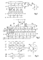
- Fig. 1 shows a simple known embodiment of a mean-forming digital-to-analog converter with a four-stage shift register sr, the series input of which is supplied with a data signal d, which consists of a pulse-density-modulated signal in binary code.
- the Q and Q 'outputs of all shift register cells are connected to a first and second summer s1, s2.
- the respective data-dependent cell current i1, i2, i3, i4 are generated from the output potential of the respective cell by means of a resistor R shown in broken lines.
- the outputs of the two summers s1, s2 are connected to a subtractor sb, which forms a differential current id. This serves as an averaging output signal, because its value is proportional to the mean of four successive logic states of the data signal d.
- the residual current id is integrated in the further processing by means of a capacitor c, from which the capacitor voltage uc can be tapped as an integral output signal.
- the two summers s1, s2 and the subtractor sb can also be adapted to the processing of voltage signals.
- the shift register sr is controlled by a clock cl, the clock rate of which is equal to the data rate of the data signal d.
- FIG. 2 shows an improved exemplary embodiment known from EP - A 0 335 988, with a division of the shift register sr into successive master and slave cells H, S.
- the master or slave cells are in this case of a first or
- the second shift cycle c1, c2 is controlled, the two shift cycles together forming a two-phase cycle, which is generally not overlapping.
- Each master and each slave cell M, S is assigned a gate circuit g which has a data-dependent control input which is connected to the Q and Q 'output of the respective shift register cell. Furthermore, each gate circuit g has a clock-dependent control input, to which an overlapping two-phase clock comprising a first and a second gate clock c3, c4, of the same frequency as the two shift clocks c1, c2, is supplied as the gate clock. The two gate cycles are phase-delayed compared to the two shift cycles so that the gate interval does not fall into the shift phase.
- each gate circuit g is assigned its own constant current source, the current of which is switched to either the Q or Q ′ gate output Q, Q ′ or to a neutral gate output due to the respective gate position.
- These neutral gate outputs are routed together via a gate current busbar sq (see FIG. 4) to a positive supply connection as a neutral current sink.
- the Q 'total current IQ' feeds the input of a current mirror cm from two identical pnp transistors.
- the output connection of this current mirror cm is connected to the Q current busbar sq, as a result of which the difference between the Q ′ and the Q total current IQ ′, IQ is formed at the connection node.
- the differential current id can thus be tapped as the output signal.
- the current distribution caused by the two transition edges must be symmetrical to the transition point E (see FIG. 3) and half at the transition point E. This determines the geometry of the transition edges, their temporal course and their phase position.
- the two transition edges intersect at a transition point E, which also defines the line of symmetry s for the current distribution.
- the overlap and thus the position of the transition point E must ensure that only a distribution of the constant current and no attenuation or suppression takes place.
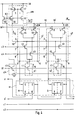
- the partial circuit diagram shown in FIG. 4 as a preferred exemplary embodiment of the invention contains a large part of the basic elements known from FIG. 1 or FIG. 2, which are provided with the corresponding reference numerals. A further detailed description is therefore unnecessary for them.
- the data signal d is fed as an antiphase signal d, d 'to the D or D' input of a first D flip-flop serving as master cell M.
- a second D flip-flop serving as slave cell S is connected to it in the usual way, and so on.
- the clock inputs of the master or slave cells are connected to the first and second shift clocks c1, c2, which together form a two-phase clock.
- the master cell M is assigned a first constant current source q1, which generates a constant current iq by means of an n-channel transistor t1 and a current source reference potential U1.
- This constant current iq is fed to a terminal 1 of the first gate circuit g1 and is by means of the two n-channel transistors t2, t3 serving as gate switches either to a first gate output, - terminal 2-, or a second or third gate output, - terminal 3 or 4 -, switched.
- the connection 3 or 4 is the Q or Q 'output Q, Q' of the first gate circuit g1.
- the connection 2 is also referred to as a neutral gate output, because the opening of this gate output depends only on the gate clock and not on the data signal d.
- connections 3 and 4 are the drain connections of an n-channel transistor pair t4, t5 serving as a second gate switch, the common source connection of which is connected to the drain connection of the transistor t3.
- the gate connection of the transistor t4 or t5 forms the connection 5 or 6 of the first gate circuit g1, which is connected to the Q or Q 'output of the master cell M.
- the connections 5 and 6 thus form the data-dependent control input of the first gate circuit g1.
- the gate connection of the transistor t2 or t3 forms the connection 7 or 8 of the first gate circuit g1 and is fed with the first or second gate signal c3, c4. Connections 7 and 8 thus together form the clock-dependent control input of the first gate circuit g1.
- the n-channel transistors t2 to t5 thus switch the supplied constant current iq to one of the three gate outputs, connection 2 or 3 or 4.
- the internal and external wiring of the second gate circuit g2 assigned to the slave cell S is identical to the first gate circuit g1 except for the activation of the n-channel transistors t2 and t3.
- the gate connection of the n-channel transistor t2 or t3 is connected to the connection 8 or 7 of the second gate circuit g2 and is thus supplied with the second or first gate clock c4, c3.
- the interconnected connections 2 of all gate circuits form a gate current bus bar sg, which is connected to the input of a current mirror cm made of p-channel transistors t6 to t9.
- the interconnected connections 4 of all gate circuits form a Q'current busbar sq ', which is connected to the output connection of the current mirror cm for forming the current difference.
- the current mirror cm has a current reduction, preferably of a factor of 0.5, from its input to the output.
- the connections 3 of all gate circuits are connected together to form a Q current busbar sq and are connected to any positive supply potential Ud 'as a current sink. The total current Ig on this current busbar sq is not used to form the differential current id.
- the main advantage of this arrangement is that the current mirror cm sees a constant total current Ig at its input, which is exactly as large as half the total current of all constant current sources q1, q2, ...
- the mirrored current Ig / 2 is therefore also a constant current.
- the data-dependent Q 'output currents iQ'M or iQ'S of the master or slave sections are then subtracted from this current mirror output current Ig / 2.
- the differential current id can then be tapped on the Q'-current busbar sq 'as the resulting signal.
- the factor of the current reduction is determined by the data reference level at which the differential current id is to become zero.
- the ratio which is formed from the value range of the data signal d below this data reference level and the total value range, indicates the current reduction factor.
- a usually symmetrical range of values gives the current reduction factor 0.5.
- the current mirror cm has no current reduction at all, e.g. if the offset direct current is equal to half the total current Ig / 2 and the data reference level lies in the middle of the total value range.
- the current mirror cm formed from the p-channel transistors t6 to t9 contains a p-channel cascode transistor t8 and t9 in the input and output. Their gate connections are common to a gate reference potential U2. This is formed by a p-channel transistor t10 connected as a diode, the common gate-source connection of which is fed by an auxiliary constant current source qh with a constant current. This auxiliary constant current source qh consists of an n-channel transistor t11, the gate connection of which is connected to the current source reference potential U1.
- the base point of the current mirror cm, which is formed by the source connections of the transistors t6 and t7, and the source connection of the transistor t10 are common to the positive supply potential Ud.
- the modulation range of the differential current id is +/- (Ig / 2), i.e. twice as large as the output current Ig / 2 of the current mirror cm. If the current mirror cm is provided with a further output which also supplies the current Ig / 2, then this connection can be used with the Q current busbar sq to form an inverted differential current.
Landscapes
- Engineering & Computer Science (AREA)
- Theoretical Computer Science (AREA)
- Analogue/Digital Conversion (AREA)
- Compression, Expansion, Code Conversion, And Decoders (AREA)
Priority Applications (5)
| Application Number | Priority Date | Filing Date | Title |
|---|---|---|---|
| EP90113417A EP0465713B1 (fr) | 1990-07-13 | 1990-07-13 | Circuit CMOS pour convertisseur numérique-analogique formateur de moyenne |
| DE59009696T DE59009696D1 (de) | 1990-07-13 | 1990-07-13 | CMOS-Schaltung für mittelwertbildende Digital-Analogumsetzer. |
| US07/706,494 US5146225A (en) | 1990-07-13 | 1991-05-28 | CMOS circuit for averaging digital-to-analog converters |
| KR1019910011755A KR100195897B1 (ko) | 1990-07-13 | 1991-07-11 | 평균화 디지털-아날로그 변환기용 cmos회로 |
| JP03174147A JP3076821B2 (ja) | 1990-07-13 | 1991-07-15 | デジタル−アナログ変換器を平均するcmos回路 |
Applications Claiming Priority (1)
| Application Number | Priority Date | Filing Date | Title |
|---|---|---|---|
| EP90113417A EP0465713B1 (fr) | 1990-07-13 | 1990-07-13 | Circuit CMOS pour convertisseur numérique-analogique formateur de moyenne |
Publications (2)
| Publication Number | Publication Date |
|---|---|
| EP0465713A1 true EP0465713A1 (fr) | 1992-01-15 |
| EP0465713B1 EP0465713B1 (fr) | 1995-09-20 |
Family
ID=8204214
Family Applications (1)
| Application Number | Title | Priority Date | Filing Date |
|---|---|---|---|
| EP90113417A Expired - Lifetime EP0465713B1 (fr) | 1990-07-13 | 1990-07-13 | Circuit CMOS pour convertisseur numérique-analogique formateur de moyenne |
Country Status (5)
| Country | Link |
|---|---|
| US (1) | US5146225A (fr) |
| EP (1) | EP0465713B1 (fr) |
| JP (1) | JP3076821B2 (fr) |
| KR (1) | KR100195897B1 (fr) |
| DE (1) | DE59009696D1 (fr) |
Families Citing this family (5)
| Publication number | Priority date | Publication date | Assignee | Title |
|---|---|---|---|---|
| US5489904A (en) * | 1993-09-28 | 1996-02-06 | The Regents Of The University Of California | Analog current mode analog/digital converter |
| US6094543A (en) * | 1997-08-25 | 2000-07-25 | Fuji Photo Film Co., Ltd. | Lens-fitted photo film unit and sprocket wheel for the same |
| US7379325B1 (en) * | 2005-12-16 | 2008-05-27 | Maxim Intergrated Products, Inc. | Non-imprinting memory with high speed erase |
| US8004441B1 (en) * | 2010-03-18 | 2011-08-23 | International Business Machines Corporation | Small-area digital to analog converter based on master-slave configuration |
| KR102216826B1 (ko) | 2017-05-22 | 2021-02-18 | (주)엘지하우시스 | 내오염성이 우수한 저광택 경화물 및 이의 제조방법 |
Citations (1)
| Publication number | Priority date | Publication date | Assignee | Title |
|---|---|---|---|---|
| EP0335988A1 (fr) * | 1988-03-31 | 1989-10-11 | Deutsche ITT Industries GmbH | Dispositif de circuit pour établir la moyenne dans un convertisseur D/A au A/D à densité d'impulsions |
Family Cites Families (2)
| Publication number | Priority date | Publication date | Assignee | Title |
|---|---|---|---|---|
| US4725813A (en) * | 1985-04-22 | 1988-02-16 | Nec Corporation | MOS type circuit device |
| US4800365A (en) * | 1987-06-15 | 1989-01-24 | Burr-Brown Corporation | CMOS digital-to-analog converter circuitry |
-
1990
- 1990-07-13 DE DE59009696T patent/DE59009696D1/de not_active Expired - Lifetime
- 1990-07-13 EP EP90113417A patent/EP0465713B1/fr not_active Expired - Lifetime
-
1991
- 1991-05-28 US US07/706,494 patent/US5146225A/en not_active Expired - Lifetime
- 1991-07-11 KR KR1019910011755A patent/KR100195897B1/ko not_active Expired - Fee Related
- 1991-07-15 JP JP03174147A patent/JP3076821B2/ja not_active Expired - Fee Related
Patent Citations (1)
| Publication number | Priority date | Publication date | Assignee | Title |
|---|---|---|---|---|
| EP0335988A1 (fr) * | 1988-03-31 | 1989-10-11 | Deutsche ITT Industries GmbH | Dispositif de circuit pour établir la moyenne dans un convertisseur D/A au A/D à densité d'impulsions |
Also Published As
| Publication number | Publication date |
|---|---|
| EP0465713B1 (fr) | 1995-09-20 |
| KR100195897B1 (ko) | 1999-06-15 |
| KR920003671A (ko) | 1992-02-29 |
| JP3076821B2 (ja) | 2000-08-14 |
| JPH04233827A (ja) | 1992-08-21 |
| DE59009696D1 (de) | 1995-10-26 |
| US5146225A (en) | 1992-09-08 |
Similar Documents
| Publication | Publication Date | Title |
|---|---|---|
| EP0335988B1 (fr) | Dispositif de circuit pour établir la moyenne dans un convertisseur D/A au A/D à densité d'impulsions | |
| EP0529119B1 (fr) | Amplificateur intégré monolithique avec commande de gain | |
| DE2555297A1 (de) | Digitalschaltung mit feldeffekttransistoren | |
| DE69117594T2 (de) | Stromschaltende logische Schaltung | |
| DE2647982A1 (de) | Logische schaltungsanordnung in integrierter mos-schaltkreistechnik | |
| EP0253914A1 (fr) | Etage driver push-pull à transistors à effet de champ à porte isolée comportant une compensation de la fluctuation des paramètres de fonctionnement et de la dispersion de fabrication | |
| DE3843365C2 (de) | Signalintegrierer | |
| DE3237778A1 (de) | Dynamisches schieberegister | |
| DE3122527A1 (de) | Stromversorgungsanordnung mit einer hochpegel-schaltverstaerkeranordnung | |
| DE4005489C2 (de) | Schaltungsanordnung für einen Digital/Analog-Wandler | |
| DE69121175T2 (de) | Flipflop-Schaltung mit einem CMOS-Hysterese-Inverter | |
| EP1004972A1 (fr) | Générateur de forme d'ondes | |
| EP0465713B1 (fr) | Circuit CMOS pour convertisseur numérique-analogique formateur de moyenne | |
| EP0986174B1 (fr) | Comparateur | |
| DE2743450A1 (de) | Sperrbare zaehlerstufe | |
| EP0360888B1 (fr) | Modulateur CMOS d'impulsions en durée | |
| DE69416554T2 (de) | Ringoszillatorschaltung für spannungsgesteuerten Oszillator mit frequenzunabhängigem Tastverhältnis | |
| DE3511688C2 (fr) | ||
| DE2201939A1 (de) | Delta-Codierer mit automatischem Ladungsabgleich | |
| EP0013686B1 (fr) | Bascule à verrouillage | |
| EP0269758B1 (fr) | Commutateur de courant | |
| EP1145443A2 (fr) | Circuit convertisseur numerique-analogique 1 bit | |
| DE19680542C2 (de) | Logiksignal-Auswahlschaltung | |
| DE2230597B2 (de) | Anordnung zur erzeugung zweier zueinander hilberttransformierter signale | |
| DE3304814A1 (de) | Differenzverstaerker |
Legal Events
| Date | Code | Title | Description |
|---|---|---|---|
| PUAI | Public reference made under article 153(3) epc to a published international application that has entered the european phase |
Free format text: ORIGINAL CODE: 0009012 |
|
| AK | Designated contracting states |
Kind code of ref document: A1 Designated state(s): DE FR GB IT NL |
|
| 17P | Request for examination filed |
Effective date: 19920620 |
|
| 17Q | First examination report despatched |
Effective date: 19950214 |
|
| GRAA | (expected) grant |
Free format text: ORIGINAL CODE: 0009210 |
|
| AK | Designated contracting states |
Kind code of ref document: B1 Designated state(s): DE FR GB IT NL |
|
| REF | Corresponds to: |
Ref document number: 59009696 Country of ref document: DE Date of ref document: 19951026 |
|
| ET | Fr: translation filed | ||
| GBT | Gb: translation of ep patent filed (gb section 77(6)(a)/1977) |
Effective date: 19951024 |
|
| ITF | It: translation for a ep patent filed | ||
| PLBE | No opposition filed within time limit |
Free format text: ORIGINAL CODE: 0009261 |
|
| STAA | Information on the status of an ep patent application or granted ep patent |
Free format text: STATUS: NO OPPOSITION FILED WITHIN TIME LIMIT |
|
| 26N | No opposition filed | ||
| REG | Reference to a national code |
Ref country code: GB Ref legal event code: IF02 |
|
| PGFP | Annual fee paid to national office [announced via postgrant information from national office to epo] |
Ref country code: GB Payment date: 20020710 Year of fee payment: 13 |
|
| PG25 | Lapsed in a contracting state [announced via postgrant information from national office to epo] |
Ref country code: GB Free format text: LAPSE BECAUSE OF NON-PAYMENT OF DUE FEES Effective date: 20030713 |
|
| GBPC | Gb: european patent ceased through non-payment of renewal fee |
Effective date: 20030713 |
|
| PG25 | Lapsed in a contracting state [announced via postgrant information from national office to epo] |
Ref country code: IT Free format text: LAPSE BECAUSE OF NON-PAYMENT OF DUE FEES;WARNING: LAPSES OF ITALIAN PATENTS WITH EFFECTIVE DATE BEFORE 2007 MAY HAVE OCCURRED AT ANY TIME BEFORE 2007. THE CORRECT EFFECTIVE DATE MAY BE DIFFERENT FROM THE ONE RECORDED. Effective date: 20050713 |
|
| PGFP | Annual fee paid to national office [announced via postgrant information from national office to epo] |
Ref country code: FR Payment date: 20090716 Year of fee payment: 20 |
|
| PGFP | Annual fee paid to national office [announced via postgrant information from national office to epo] |
Ref country code: NL Payment date: 20090730 Year of fee payment: 20 Ref country code: DE Payment date: 20090722 Year of fee payment: 20 |
|
| REG | Reference to a national code |
Ref country code: NL Ref legal event code: V4 Effective date: 20100713 |
|
| PG25 | Lapsed in a contracting state [announced via postgrant information from national office to epo] |
Ref country code: NL Free format text: LAPSE BECAUSE OF EXPIRATION OF PROTECTION Effective date: 20100713 |
|
| PG25 | Lapsed in a contracting state [announced via postgrant information from national office to epo] |
Ref country code: DE Free format text: LAPSE BECAUSE OF EXPIRATION OF PROTECTION Effective date: 20100713 |